EP3240027A1 - Conditionnement de semi-conducteur - Google Patents
Conditionnement de semi-conducteur Download PDFInfo
- Publication number
- EP3240027A1 EP3240027A1 EP16166904.9A EP16166904A EP3240027A1 EP 3240027 A1 EP3240027 A1 EP 3240027A1 EP 16166904 A EP16166904 A EP 16166904A EP 3240027 A1 EP3240027 A1 EP 3240027A1
- Authority
- EP
- European Patent Office
- Prior art keywords
- substrate
- cavity
- semiconductor
- cavities
- electric contact
- Prior art date
- Legal status (The legal status is an assumption and is not a legal conclusion. Google has not performed a legal analysis and makes no representation as to the accuracy of the status listed.)
- Granted
Links
Images


Classifications
-
- H—ELECTRICITY
- H10—SEMICONDUCTOR DEVICES; ELECTRIC SOLID-STATE DEVICES NOT OTHERWISE PROVIDED FOR
- H10W—GENERIC PACKAGES, INTERCONNECTIONS, CONNECTORS OR OTHER CONSTRUCTIONAL DETAILS OF DEVICES COVERED BY CLASS H10
- H10W40/00—Arrangements for thermal protection or thermal control
- H10W40/20—Arrangements for cooling
- H10W40/22—Arrangements for cooling characterised by their shape, e.g. having conical or cylindrical projections
-
- H—ELECTRICITY
- H10—SEMICONDUCTOR DEVICES; ELECTRIC SOLID-STATE DEVICES NOT OTHERWISE PROVIDED FOR
- H10W—GENERIC PACKAGES, INTERCONNECTIONS, CONNECTORS OR OTHER CONSTRUCTIONAL DETAILS OF DEVICES COVERED BY CLASS H10
- H10W40/00—Arrangements for thermal protection or thermal control
- H10W40/20—Arrangements for cooling
- H10W40/25—Arrangements for cooling characterised by their materials
- H10W40/255—Arrangements for cooling characterised by their materials having a laminate or multilayered structure, e.g. direct bond copper [DBC] ceramic substrates
-
- H—ELECTRICITY
- H10—SEMICONDUCTOR DEVICES; ELECTRIC SOLID-STATE DEVICES NOT OTHERWISE PROVIDED FOR
- H10W—GENERIC PACKAGES, INTERCONNECTIONS, CONNECTORS OR OTHER CONSTRUCTIONAL DETAILS OF DEVICES COVERED BY CLASS H10
- H10W74/00—Encapsulations, e.g. protective coatings
- H10W74/10—Encapsulations, e.g. protective coatings characterised by their shape or disposition
- H10W74/111—Encapsulations, e.g. protective coatings characterised by their shape or disposition the semiconductor body being completely enclosed
- H10W74/124—Encapsulations, e.g. protective coatings characterised by their shape or disposition the semiconductor body being completely enclosed the encapsulations having cavities other than that occupied by chips
-
- H—ELECTRICITY
- H10—SEMICONDUCTOR DEVICES; ELECTRIC SOLID-STATE DEVICES NOT OTHERWISE PROVIDED FOR
- H10W—GENERIC PACKAGES, INTERCONNECTIONS, CONNECTORS OR OTHER CONSTRUCTIONAL DETAILS OF DEVICES COVERED BY CLASS H10
- H10W90/00—Package configurations
-
- H—ELECTRICITY
- H02—GENERATION; CONVERSION OR DISTRIBUTION OF ELECTRIC POWER
- H02P—CONTROL OR REGULATION OF ELECTRIC MOTORS, ELECTRIC GENERATORS OR DYNAMO-ELECTRIC CONVERTERS; CONTROLLING TRANSFORMERS, REACTORS OR CHOKE COILS
- H02P27/00—Arrangements or methods for the control of AC motors characterised by the kind of supply voltage
- H02P27/04—Arrangements or methods for the control of AC motors characterised by the kind of supply voltage using variable-frequency supply voltage, e.g. inverter or converter supply voltage
- H02P27/06—Arrangements or methods for the control of AC motors characterised by the kind of supply voltage using variable-frequency supply voltage, e.g. inverter or converter supply voltage using DC to AC converters or inverters
- H02P27/08—Arrangements or methods for the control of AC motors characterised by the kind of supply voltage using variable-frequency supply voltage, e.g. inverter or converter supply voltage using DC to AC converters or inverters with pulse width modulation
-
- H—ELECTRICITY
- H10—SEMICONDUCTOR DEVICES; ELECTRIC SOLID-STATE DEVICES NOT OTHERWISE PROVIDED FOR
- H10W—GENERIC PACKAGES, INTERCONNECTIONS, CONNECTORS OR OTHER CONSTRUCTIONAL DETAILS OF DEVICES COVERED BY CLASS H10
- H10W70/00—Package substrates; Interposers; Redistribution layers [RDL]
- H10W70/60—Insulating or insulated package substrates; Interposers; Redistribution layers
- H10W70/611—Insulating or insulated package substrates; Interposers; Redistribution layers for connecting multiple chips together
- H10W70/614—Insulating or insulated package substrates; Interposers; Redistribution layers for connecting multiple chips together the multiple chips being integrally enclosed
-
- H—ELECTRICITY
- H10—SEMICONDUCTOR DEVICES; ELECTRIC SOLID-STATE DEVICES NOT OTHERWISE PROVIDED FOR
- H10W—GENERIC PACKAGES, INTERCONNECTIONS, CONNECTORS OR OTHER CONSTRUCTIONAL DETAILS OF DEVICES COVERED BY CLASS H10
- H10W70/00—Package substrates; Interposers; Redistribution layers [RDL]
- H10W70/60—Insulating or insulated package substrates; Interposers; Redistribution layers
- H10W70/67—Insulating or insulated package substrates; Interposers; Redistribution layers characterised by their insulating layers or insulating parts
- H10W70/69—Insulating materials thereof
- H10W70/698—Semiconductor materials that are electrically insulating, e.g. undoped silicon
-
- H—ELECTRICITY
- H10—SEMICONDUCTOR DEVICES; ELECTRIC SOLID-STATE DEVICES NOT OTHERWISE PROVIDED FOR
- H10W—GENERIC PACKAGES, INTERCONNECTIONS, CONNECTORS OR OTHER CONSTRUCTIONAL DETAILS OF DEVICES COVERED BY CLASS H10
- H10W72/00—Interconnections or connectors in packages
- H10W72/071—Connecting or disconnecting
- H10W72/073—Connecting or disconnecting of die-attach connectors
- H10W72/07331—Connecting techniques
-
- H—ELECTRICITY
- H10—SEMICONDUCTOR DEVICES; ELECTRIC SOLID-STATE DEVICES NOT OTHERWISE PROVIDED FOR
- H10W—GENERIC PACKAGES, INTERCONNECTIONS, CONNECTORS OR OTHER CONSTRUCTIONAL DETAILS OF DEVICES COVERED BY CLASS H10
- H10W76/00—Containers; Fillings or auxiliary members therefor; Seals
- H10W76/60—Seals
-
- H—ELECTRICITY
- H10—SEMICONDUCTOR DEVICES; ELECTRIC SOLID-STATE DEVICES NOT OTHERWISE PROVIDED FOR
- H10W—GENERIC PACKAGES, INTERCONNECTIONS, CONNECTORS OR OTHER CONSTRUCTIONAL DETAILS OF DEVICES COVERED BY CLASS H10
- H10W90/00—Package configurations
- H10W90/401—Package configurations characterised by multiple insulating or insulated package substrates, interposers or RDLs
-
- H—ELECTRICITY
- H10—SEMICONDUCTOR DEVICES; ELECTRIC SOLID-STATE DEVICES NOT OTHERWISE PROVIDED FOR
- H10W—GENERIC PACKAGES, INTERCONNECTIONS, CONNECTORS OR OTHER CONSTRUCTIONAL DETAILS OF DEVICES COVERED BY CLASS H10
- H10W90/00—Package configurations
- H10W90/701—Package configurations characterised by the relative positions of pads or connectors relative to package parts
- H10W90/731—Package configurations characterised by the relative positions of pads or connectors relative to package parts of die-attach connectors
- H10W90/735—Package configurations characterised by the relative positions of pads or connectors relative to package parts of die-attach connectors between a chip and a laterally-adjacent insulating package substrate, interposer or RDL
-
- H—ELECTRICITY
- H10—SEMICONDUCTOR DEVICES; ELECTRIC SOLID-STATE DEVICES NOT OTHERWISE PROVIDED FOR
- H10W—GENERIC PACKAGES, INTERCONNECTIONS, CONNECTORS OR OTHER CONSTRUCTIONAL DETAILS OF DEVICES COVERED BY CLASS H10
- H10W95/00—Packaging processes not covered by the other groups of this subclass
Definitions
- the invention relates to a semiconductor package which comprises a first substrate and a second substrate, wherein between the first and the second substrate a plurality of cavities is formed, each of the cavities having a bottom wall and side walls, and a plurality of semiconductor elements, wherein at least one of the semiconductor elements is placed within a corresponding cavity and wherein the first and the second substrate are attached to each other thereby encapsulating the semiconductor elements located within the corresponding cavities.
- the invention is useful for any particular semiconductor element, where a hermetic encapsulation would be helpful and where heat dissipation during use is needed.
- the semiconductor element is a semiconductor die, i.e. is a small block of semiconducting material, on which a given functional circuit is fabricated.
- the semiconductor element is, for example, one of a diode, a diac, a triac, a thyristor, a transistor, an IGBT and a MOSFET.
- the semiconductor element is particularly used as a switch or rectifier in power electronics.
- the invention relates to a power semiconductor element. More particularly, the invention relates to packed semiconductor elements for switching or rectifying currents and/or voltages for drives in electro mobility. Generally, the invention relates to the technical field of microelectronics, particularly to a stacked package of semiconductor elements.
- a semiconductor package of the aforementioned type is disclosed, for example, in US 7,026,223 B2 and in US 2007/0166958 A1 .
- a package is disclosed that comprises a base and a lid, wherein a hermetically sealed cavity is formed therebetween and wherein a semiconductor element is placed within the cavity.
- the base includes conductive vias extending therethrough and the semiconductor element is electrically connected through the vias from the outer side of the base. Any further conductive pathes through the junction between the base and the lid are avoided.
- the package shown in US 7,026,223 B2 can be produced at a wafer level using conventional silicon wafer integrated circuit manufacturing machinery prior to separating the wafer into a plurality of devices.
- a package comprising a packaging wafer and an element wafer, wherein the packaging wafer comprises a plurality of cavities on an upper surface, wherein the element wafer comprises a plurality of semiconductor elements and wherein the packaging wafer and the element wafer are bonded to each other thereby enclosing the semiconductor elements.
- the packaging wafer comprises a plurality of cavities on an upper surface
- the element wafer comprises a plurality of semiconductor elements and wherein the packaging wafer and the element wafer are bonded to each other thereby enclosing the semiconductor elements.
- the openings in the membrane are hermetically sealed by metal plating.
- conductive paths are formed which run from the micro-vias along the side walls of the cavity to the front side of the cap.
- the cap is placed with its cavity onto the semiconductor element which is bonded to a circuit board adapted in size and form, and the cap is soldered to the circuit board by a sealing ring which surrounds the cavity.
- the encapsulated semiconductor element is electrically connected from the backside of the cap over the vias and over the conductive paths along the inner side walls of the cavity which are electrically connected with metallization lines of the circuit board to which the semiconductor element is bonded. No direct electrical contact is given at the backside of the semiconductor element.
- the dominating electrical connection of semiconductor elements is direct and wire bonding.
- Wire bonding causes additional inductance by the bond loops which cause parasitic effects like high voltage peaks when switching the element. High voltage peaks can cause failures during operation and a faster degradation thereby reducing the reliability of the device. Accordingly, a replacement of the wire bonds will increase the reliability.
- solder or other bonding materials are deposited on the contact pads of the semiconductor element.
- For mounting the semiconductor element to a circuit board or substrate it is flipped over so that its top side faces down and the solder bumps at the pads are aligned with matching pads on the circuit board. In a subsequent reflow process the pads of the semiconductor element and the pads of the circuit board then become soldered.
- This problem is solved, as already mentioned above, in a known manner by packages which encapsulate or hermetically seal a semiconductor element placed therein. Use of such packages will increase the lifetime of the semiconductor elements but will also cause additional costs.
- the encapsulated semiconductor element is electrically contacted with the aid of electrical vias through the package which are filled with metal. The fabrication of the vias has to be implemented as an additional production step and increases the costs on the whole.
- this object is solved by providing a semiconductor package, the package comprising a first substrate comprising at a front cavity side a plurality of cavities, each of the cavities having a bottom wall and side walls, and having a conductive path forming an electric contact surface located at the inner side of the bottom wall of the cavity, a plurality of semiconductor elements, each of the semiconductor elements comprising a first electric contact surface on a first side and a second electric contact surface on a second side opposite to the first side, wherein at least one of the semiconductor elements is placed within a corresponding cavity at the cavity side of the first substrate, wherein the first electric contact of the semiconductor element and the electric contact surface at the inner side of the bottom wall of the corresponding cavity are electrically conductive bonded in a material-locking manner, and a second substrate, the second substrate being attached with a connection side to the front cavity side of the first substrate thereby encapsulating the semiconductor elements located within the corresponding cavities at the front cavity side of the first substrate.
- the invention starts with the idea to provide a semiconductor package that is completely mountable on wafer level.
- Any conventional semiconductor wafer e.g. a silicon wafer, and/or a conventional ceramic tile can be used as a substrate.
- the invention also allows for integrate a plurality of active and passive electric components within the encapsulated cavities.
- the invention allows to stack semiconductor elements in cavities of different substrates and to electrically connect them directly, for example, through conductive vias extending through a substrate.
- the invention also provides a layer between the substrates for electrical connection of the elements or components placed within the cavities.
- the outer sides of the semiconductor package are electrically insulated from an inner side, which allows for excellent direct heat dissipation through the substrate by attaching a heat sink on at least one of the outer sides of the package.
- the assembled package is separated into several packages by a subsequent cutting step.
- the semiconductor elements and also other active or passive electric components can be added and bonded at the wafer level using conventional wafer integrated circuit manufacturing machinery. Any conventional die or flip-chip wafer level bonding process may be used.
- the semiconductor elements, additional electric components and the substrates are preferably bonded by a soldering or sintering process. An eutectic soldering process may be used. A transient liquid phase soldering is preferred due to its lower process temperature.
- a silicon wafer is used as at least one of the substrates. According to a preferred embodiment the cavities are fabricated by a dry or wet etching process.
- Electrical conductive paths along the substrates can be fabricated by a lithographic process combined with metal deposition like electroless plating or electroplating, a CVD or a PVD process. Other processes like direct laser ablation, plasma deposition, dispensing, jetting or printing of conductive material might be also used.
- the process of attaching the semiconductor elements and further electric components within the cap and of attaching the substrates to each other is preferably performed on a wafer level.
- the semiconductor package further comprises a third substrate that is attached with a connection side to the first substrate or to the second substrate, respectively.
- a third substrate at least two layers at the connection sides interconnecting two of the third substrates are provided for electrical connection of the semiconductor elements and other electric components, respectively.
- the second substrate comprises two opposed connection sides
- the third substrate further comprises on a cavity side which is the connection side a plurality of cavities, each of the cavities having a bottom wall and side walls, and having a conductive path forming an electric contact surface located at the inner side of the bottom wall of the cavity, wherein at least one of the plurality of semiconductor elements is placed within a corresponding cavity at the cavity side of the third substrate, wherein the first electric contact of the semiconductor element and the electric contact surface at the inner side of the bottom wall of the corresponding cavity are electrically conductive bonded in a material-locking manner, and wherein the third substrate is attached with the cavity side to a connection side of the second substrate thereby encapsulating the semiconductor elements located within the corresponding cavities at the cavity side of the third substrate.
- the second substrate is an intermediate substrate carrying the first and the second substrate on its both sides.
- the first substrate as well as the third substrate comprise cavities and are connected with its respective cavity sides at one of the connection sides of the second substrate, respectively.
- two structured conductive layers are provided at the connection sides of the second substrate.
- the second substrate is a semiconductor wafer with a thickness that is smaller than the thickness of the first and the third substrate.
- the second substrate is a silicon wafer with a thickness between 20 and 100 ⁇ m.
- Conductive vias are fabricated by known methods, for example, by wet etching or dry etching, particularly reactive ion etching. In a subsequent step, metal is brought into the vias by PVC, CVD or by electroplating.
- the first and the third substrate are particularly made from a semiconductor or from a ceramics.
- a semiconductor wafer or a ceramic tile is used.
- the first and/or the third substrate are produced as a multi-layer ceramic tile, for example, by attaching the different ceramic layers with a sintering process.
- the cavities can be fabricated by already known methods like dry or wet etching, particularly ion etching.
- the first substrate further comprises also on a back cavity side opposite to the front cavity side a plurality of cavities, each of the cavities having a bottom wall and side walls, and having a conductive path forming an electric contact surface located at the inner side of the bottom wall of the cavity, wherein at least one of the plurality of semiconductor elements is placed within a corresponding cavity at the back cavity side of the first substrate, wherein the first electric contact of the semiconductor element and the electric contact surface at the inner side of the bottom wall of the corresponding cavity are electrically conductive bonded in a material-locking manner, and wherein the third substrate is attached with the connection side to the back cavity side of the first substrate thereby encapsulating the semiconductor elements located within the corresponding cavities at the back cavity side of the first substrate.
- This second embodiment of the invention provides for two flat, unstructured outer substrates, i.e. the second and the third substrate. Accordingly, commercially available low cost semiconductor wafer can be implemented.
- a flat ceramic substrate for example a DBC ceramic is used as the second and/or the third substrate.
- the first substrate in this second embodiment is a substrate that is structured with cavities on both sides.
- conductive vias are brought into the substrate by already known methods, as explained above.
- a wet etching process is preferred that allows fabrication of cavities on both sides of the substrate in a common fabrication step.
- a SOI wafer silicon/silicon dioxide/silicon
- the intermediate glass layer functions as a stop during the etching process.
- a conventional semiconductor wafer can be used and the cavities are produced by a timely controlled etching process. Remaining differences in the thickness of the bottom walls of the cavities may be tolerated by the process to be used for bonding the semiconductor elements or other electric components at the bottom wall within the cavity.
- the first substrate is produced by bonding two structured semiconductor wafers to each other.
- no silicon remains between the electric components placed in opposed cavities.
- Metallic traces are fabricated on the outer sides of both of the semiconductor wafers and subsequently, the semiconductor wafers are bonded to each other with its inner silicon sides.
- cavities through both wafers are fabricated by an etching process.
- the first substrate according to another preferred alternative can be also made from a multi-layer ceramic tile.
- a multi-layer composing process cavities as well as vias can be fabricated in an already known manner.
- the second substrate further comprises on a cavity side a plurality of cavities, each of the cavities having a bottom wall and side walls, and having a conductive path forming an electric contact surface located at the inner side of the bottom wall of the cavity, wherein at least one of the plurality of semiconductor elements is placed within a corresponding cavity at the cavity side of the second substrate, wherein the first electric contact of the semiconductor element and the electric contact at the inner side of the bottom wall of the corresponding cavity are electrically conductive bonded in a material-locking manner, and wherein the third substrate is attached with the connection side to the cavity side of the second substrate thereby encapsulating the semiconductor elements located within the corresponding cavities at the cavity side of the first substrate.
- This third embodiment of the invention uses two similar substrates, i.e. the first substrate and the second substrate, which are stacked one on top of the other.
- the intermediate second substrate covers the cavities within the first substrate.
- the third substrate covers the cavities of the second substrate.
- the first and the second substrates are similar and are made, preferably, from a semiconductor wafer or a ceramic tile as already explained above.
- the cavities within the second substrate are fabricated without remaining substrate substance at the bottom wall.
- the bottom walls of these cavities of the second substrate are constituted by a remaining metallization or conductive area.
- the third substrate is, for example, a low cost flat wafer like an unstructured semiconductor wafer or is a flat ceramic tile.
- the total hight of the cavity matches the total hight of the semiconductor element placed therein so that the second side of the semiconductor element is aligned with the cavity side.
- the second side of the semiconductor element is leveled with the edge of the substrate surrounding the cavity.
- transient liquid phase soldering and soft soldering are preferred methods allowing leveling of the surfaces of the components to be bonded.
- the invention does also cover the embodiment that several semiconductor elements and/or electric components are placed within one single cavity.
- the semiconductor element comprises a first, a second and a third electric contact.
- the semiconductor element is placed with the side into the cavity that comprises one single electric contact.
- a machinery tool may be used for placing the semiconductor elements or other electric components into the cavity that comprises distance elements for leveling the surface of the semiconductor element and/or of the electric component with the edges of the substrate surrounding the cavity.
- a difference in hight between the cavity and the semiconductor element or the electronic component is leveled by the thickness of the solder or sintering material placed at the bottom wall within the cavity.
- At least one portion of the conductive path of at least one of the cavities is attached to the inner side of at least one of the side walls of said at least one cavity.
- the conductive paths which are routed along the inner side of the cavity can be fabricated by a lithographic process combined with metal deposition, like electroless plating or electroplating, a CVD or PVD process. Other processes like direct laser ablation, plasma deposition, dispensing, jetting or printing of conductive material might be also used.
- the conductive path along the inner side of the cavity is used to electrically contact the first electric contact located at the first side of the semiconductor element at the bottom wall of the cavity.
- the conductive path is impedance matched by its electrical routing within the cavity.
- the direct connection of the first electrical contact at the first side of the semiconductor elements provides low parasitic impedance.
- the direct interconnection also increases the transfer of heat from the semiconductor element to the substrate. This additional increases the reliability of the device.
- disjunct electrically conductive areas are comprised and wherein the conductive path of at least one of the cavities of said cavity sides extends between the corresponding electric surface located at the inner side of the bottom wall of said at least one cavity and at least one of the disjunct conductive areas at said cavity side.
- the disjunct electrically conductive areas provide for the electric connection of the elements and components placed within the cavities.
- the second electric contact surface at the second side of at least one of the semiconductor elements and at least one of the conductive areas at the connection side of at least one substrate are electrically conductive bonded in a material-locking manner. This direct bonding allows for increasing the heat transfer from a semiconductor element to the substrate as already described above.
- At least one of the disjunct electrically conductive areas at the cavity side of at least one of the substrates and at least one of the disjunct electrical conductive areas at the connection side of another substrate are electrically conductive bonded in a material-locking manner.
- all substrates are connected in a common sintering or soldering process.
- At least one of the substrates is extending with a contact region beyond another substrate, wherein the contact region comprises at least one electrically conductive region which is electrically conductive connected with at least one of the electrically conductive areas.
- This embodiment provides a freely accessible contact area for the electrical connection of the semiconductor elements and electric components within the package.
- At least one first cavity with a first semiconductor element placed therein and at least one second cavity with a second semiconductor element placed therein are located on top of each other, wherein at least one electric contact of the first semiconductor element and at least one electric contact of the second semiconductor element are electrically conductive bonded to each other in a material-locking manner.
- This embodiment allows for direct stacking of semiconductor elements and other electric components. By a direct electrical contact between the stacked semiconductor elements and components additional inductance by bond loops of vias is avoided.
- the respective electric contacts of the first semiconductor element and of the second semiconductor element are bonded to each other through vias located in one of the substrates or through at least one of the disjunct electrically conductive areas.
- the package further comprises a plurality of passive electric components, at least one of said passive electrical components being placed within a corresponding cavity.
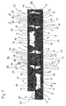
- Figure 1 shows a first embodiment of a semiconductor package 1 wherein a first substrate 2 is placed above an intermediate second substrate 3 to which on an upper side a third substrate 4 is attached.
- the first substrate 2 and the third substrate 4 both comprise at its inner sides, which are further referred to also as cavity sides 5, a plurality of cavities 6, 6' each of which comprises a bottom wall 7 and side walls 8.
- a semiconductor wafer is used as the first substrate 2 and/or as the third substrate 4 and the cavities 6, 6' are fabricated by dry etching.
- the first substrate 2 and/or the third substrate 4 may be fabricated as a multi-layer ceramic tile.
- electric contact surfaces 9 are provided which are connected to a conductive path 10 which is attached to the inner side of a side wall 8 of the respective cavity 6, 6'.
- the conductive paths 10 extending along the inner side of the cavities 6, 6' and are electrically connected to at least one of disjunct electrical conductive areas 11 which are attached at the cavity sides 5 of the first substrate 2 and the third substrate 4.
- the second substrate 3 has a thickness that is smaller than the thickness of the first substrate 2 and the third substrate 4.
- a thin flat semiconductor wafer is used as the second substrate 3.
- the second substrate 3 on both sides comprises also disjunct electrical conductive areas 11 which are attached to the surface of the substrate 3 in an already known manner.
- Each side of the second substrate 3 provides a connection side 12, 13, respectively.
- the disjunct electrical conductive areas 11 at the first connection side 12 and at the second connection side 13 of the second substrate 3 are bonded to the respective disjunct electrical conductive areas 11 at the cavity sides 5 of the first substrate 2 and of the third substrate 4.
- the bonding process is, for example, a soldering process, wherein a solder 14 is placed between the respective conductive areas 11 at the locations to become bonded.
- first semiconductor elements 16 and second semiconductor elements 17 and passive electric components 18 are located within the cavities 6, 6'.
- the semiconductor elements 16, 17 and the passive electric components 18 placed within the cavities 6, 6' are bonded with its respective electric contacts with the electric contact surface 9 at the bottom wall 7 of the respective cavities 6, 6'.
- For the semiconductor elements 16, 17 its respective first side 26 and its respective first electric contact 27 are shown. Any useful bonding process described above can be used to fix the components and elements within the cavity 6, 6'.
- On its respective second side 28 the semiconductor elements 16, 17 and the passive electric components 18 are bonded with its respective electric contacts 29 to at least one of the disjunct electrical conductive areas 11 at the connection sides 12, 13 of the second substrate 3.
- the contact region 20 comprises a freely accessible conductive region 21 which is connected with at least one of the electrical conductive areas 11 within the package 1.
- the second substrate 3 additionally comprises electrically conductive vias 19 which are provided between the stacked semiconductor elements 6, 6'. This allows a direct stacking of the semiconductor elements 6, 6' where its respective electrical contacts are directly connected. Additional inductance induced by wire bonding is avoided.
- the vias are fabricated by known fabricating processes as already described above.
- the first substrate 2 extends with a contact region 20 beyond the second substrate 3 and the third substrate 4. On the contact region 20 of the first substrate 2 a freely accessible conductive region 21 is provided.
- Figure 2 depicts a second embodiment of a semiconductor package 1'.
- the semiconductor package 1' according to Figure 2 differs from the semiconductor package 1 shown in Figure 1 in that the first substrate 2 which comprises the cavities 6, 6' is an intermediate substrate which comprises at its both sides, i.e. a front cavity side 5 and a back cavity side 22, cavities 6, 6'.
- the intermediate first substrate 2 of the semiconductor package 1' is a semiconductor wafer.
- a multi-layer ceramic tile is used.
- conductive vias 19 are comprised which allow a direct electrical connection of the respective contacts 27, 29 of the semiconductor elements 16, 17 and the electric components 18 through the first substrate 2.
- the second substrate 3 and the third substrate 4 are flat outer substrates which do not comprise any cavity.
- a conventional thin unstructured semiconductor wafer is preferably used as the second substrate 3 and the third substrate 4.
- Figure 3 shows in a third embodiment a semiconductor package 1 ", where the first substrate 2 and the second substrate 3 are similar to each other and do both comprise cavities 6, 6'.
- the cavities 6, 6' within the second substrate 3 are fabricated without remaining substrate substance at the bottom wall 7.
- the bottom walls 7 of the cavities 6, 6' of the second substrate 3 are constituted by a remaining metallization or conductive area 11.
- the semiconductor elements 16 and 17 are stacked within the cavities 6, 6' on top of each other.
- the respective contacts 27, 29 of the semiconductor elements 17, 18 are directly electrically conducted through interposed conductive areas 11.
- the second substrate 3 and the third substrate 4 both extend with a contact region 20 beyond the first substrate 2. On the contact region 20 of the second substrate 3 and the third substrate 4 freely accessible conductive regions 21 are provided.
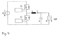
- Figure 4 depicts an electronic circuitry which comprises a half-bridge in a DC voltage link.
- the half-bridge comprises a first semiconductor element 16 and a second semiconductor element 17.
- the semiconductor elements 16 and 17 both comprise a switching element, for example, a MOSFET or an IGBT.
- the switching elements are bridged by a free-wheeling diode, respectively.
- the drawn boxes stand for control modules which control the switching elements.
- the shown half-bridge is typically used in electronics, for example, to convert a DC voltage into a AC voltage by pulse width modulation (PWM).
- the AC output voltage is used, for example, as one phase of an electric machine R, like an electric motor. Additional inductors L and capacitors C may be also provided.
- the semiconductor elements 16 comprising at least the switching elements and its respective bridging diodes may be fabricated as a semiconductor die.
- the switching elements or the respective semiconductor elements 16, 17 are stacked one on top of the other in the cavities 6, 6' of a semiconductor package according to one of the Figures 1 to 3 .
- the circuitry shown in Figure 4 including also the passive electric components is preferably realized as a semiconductor package according to the invention.
Landscapes
- Micromachines (AREA)
- Chemical & Material Sciences (AREA)
- Engineering & Computer Science (AREA)
- Ceramic Engineering (AREA)
Priority Applications (3)
| Application Number | Priority Date | Filing Date | Title |
|---|---|---|---|
| EP16166904.9A EP3240027B1 (fr) | 2016-04-25 | 2016-04-25 | Conditionnement de semi-conducteur |
| PCT/EP2017/059627 WO2017186627A1 (fr) | 2016-04-25 | 2017-04-24 | Boîtier à semi-conducteurs |
| US16/092,454 US10692796B2 (en) | 2016-04-25 | 2017-04-24 | Semiconductor package having stacked substrates with cavities |
Applications Claiming Priority (1)
| Application Number | Priority Date | Filing Date | Title |
|---|---|---|---|
| EP16166904.9A EP3240027B1 (fr) | 2016-04-25 | 2016-04-25 | Conditionnement de semi-conducteur |
Publications (2)
| Publication Number | Publication Date |
|---|---|
| EP3240027A1 true EP3240027A1 (fr) | 2017-11-01 |
| EP3240027B1 EP3240027B1 (fr) | 2021-03-17 |
Family
ID=55808514
Family Applications (1)
| Application Number | Title | Priority Date | Filing Date |
|---|---|---|---|
| EP16166904.9A Not-in-force EP3240027B1 (fr) | 2016-04-25 | 2016-04-25 | Conditionnement de semi-conducteur |
Country Status (3)
| Country | Link |
|---|---|
| US (1) | US10692796B2 (fr) |
| EP (1) | EP3240027B1 (fr) |
| WO (1) | WO2017186627A1 (fr) |
Cited By (1)
| Publication number | Priority date | Publication date | Assignee | Title |
|---|---|---|---|---|
| CN110241403A (zh) * | 2019-07-23 | 2019-09-17 | 芜湖通潮精密机械股份有限公司 | 一种减小温差的加热器及其制作方法和应用 |
Families Citing this family (11)
| Publication number | Priority date | Publication date | Assignee | Title |
|---|---|---|---|---|
| WO2015006421A1 (fr) | 2013-07-09 | 2015-01-15 | United Technologies Corporation | Article polymère sous encapsulation métallique |
| WO2015017095A2 (fr) | 2013-07-09 | 2015-02-05 | United Technologies Corporation | Coiffe polymère plaquée |
| US10927843B2 (en) | 2013-07-09 | 2021-02-23 | Raytheon Technologies Corporation | Plated polymer compressor |
| WO2015006452A1 (fr) * | 2013-07-09 | 2015-01-15 | United Technologies Corporation | Composants de transmission et de moteur de véhicule réalisés en polymères plaqués |
| CA2917884A1 (fr) | 2013-07-09 | 2015-01-15 | United Technologies Corporation | Ventilateur en polymere plaque |
| JP7025948B2 (ja) * | 2018-02-13 | 2022-02-25 | ローム株式会社 | 半導体装置および半導体装置の製造方法 |
| DE102019103281B4 (de) | 2019-02-11 | 2023-03-16 | Infineon Technologies Ag | Verfahren zum bilden eines die-gehäuses |
| SG10201904605WA (en) * | 2019-05-23 | 2020-12-30 | Delta Electronics Int’L Singapore Pte Ltd | Package structure |
| US11532563B2 (en) * | 2020-09-21 | 2022-12-20 | Apple Inc. | Package integration using fanout cavity substrate |
| DE102021101010A1 (de) | 2021-01-19 | 2022-07-21 | Infineon Technologies Ag | Vorgehäuster chip, verfahren zum herstellen eines vorgehäusten chips, halbleitergehäuse und verfahren zum herstellen eines halbleitergehäuses |
| EP4290574A1 (fr) * | 2022-06-09 | 2023-12-13 | Mitsubishi Electric R&D Centre Europe B.V. | Module de puissance avec cartes de puissance et barre omnibus de carte de circuit imprimé intégrées |
Citations (6)
| Publication number | Priority date | Publication date | Assignee | Title |
|---|---|---|---|---|
| US7026223B2 (en) | 2002-03-28 | 2006-04-11 | M/A-Com, Inc | Hermetic electric component package |
| US20060198570A1 (en) * | 2005-02-28 | 2006-09-07 | Tsuyoshi Ogawa | Hybrid module and production method for same, and hybrid circuit device |
| US20070166958A1 (en) | 2006-01-18 | 2007-07-19 | Shun-Ta Wang | Method of wafer level packaging and cutting |
| US20120146177A1 (en) * | 2010-12-09 | 2012-06-14 | Stats Chippac, Ltd. | Semiconductor Device and Method of Forming Recesses in Substrate for Same Size or Different Sized Die with Vertical Integration |
| US20150262902A1 (en) * | 2014-03-12 | 2015-09-17 | Invensas Corporation | Integrated circuits protected by substrates with cavities, and methods of manufacture |
| DE102014114982A1 (de) * | 2014-10-15 | 2016-04-21 | Infineon Technologies Ag | Verfahren zum Bilden einer Chip-Baugruppe und Chip-Baugruppe |
Family Cites Families (5)
| Publication number | Priority date | Publication date | Assignee | Title |
|---|---|---|---|---|
| US10199321B2 (en) * | 2015-09-03 | 2019-02-05 | Bridge Semiconductor Corporation | Interconnect substrate having cavity for stackable semiconductor assembly, manufacturing method thereof and vertically stacked semiconductor assembly using the same |
| US9355997B2 (en) * | 2014-03-12 | 2016-05-31 | Invensas Corporation | Integrated circuit assemblies with reinforcement frames, and methods of manufacture |
| US9252127B1 (en) * | 2014-07-10 | 2016-02-02 | Invensas Corporation | Microelectronic assemblies with integrated circuits and interposers with cavities, and methods of manufacture |
| US9478504B1 (en) * | 2015-06-19 | 2016-10-25 | Invensas Corporation | Microelectronic assemblies with cavities, and methods of fabrication |
| US10256173B2 (en) * | 2016-02-22 | 2019-04-09 | Advanced Semiconductor Engineering, Inc. | Semiconductor device and method for manufacturing the same |
-
2016
- 2016-04-25 EP EP16166904.9A patent/EP3240027B1/fr not_active Not-in-force
-
2017
- 2017-04-24 WO PCT/EP2017/059627 patent/WO2017186627A1/fr not_active Ceased
- 2017-04-24 US US16/092,454 patent/US10692796B2/en not_active Expired - Fee Related
Patent Citations (6)
| Publication number | Priority date | Publication date | Assignee | Title |
|---|---|---|---|---|
| US7026223B2 (en) | 2002-03-28 | 2006-04-11 | M/A-Com, Inc | Hermetic electric component package |
| US20060198570A1 (en) * | 2005-02-28 | 2006-09-07 | Tsuyoshi Ogawa | Hybrid module and production method for same, and hybrid circuit device |
| US20070166958A1 (en) | 2006-01-18 | 2007-07-19 | Shun-Ta Wang | Method of wafer level packaging and cutting |
| US20120146177A1 (en) * | 2010-12-09 | 2012-06-14 | Stats Chippac, Ltd. | Semiconductor Device and Method of Forming Recesses in Substrate for Same Size or Different Sized Die with Vertical Integration |
| US20150262902A1 (en) * | 2014-03-12 | 2015-09-17 | Invensas Corporation | Integrated circuits protected by substrates with cavities, and methods of manufacture |
| DE102014114982A1 (de) * | 2014-10-15 | 2016-04-21 | Infineon Technologies Ag | Verfahren zum Bilden einer Chip-Baugruppe und Chip-Baugruppe |
Non-Patent Citations (1)
| Title |
|---|
| A. HAUFFE; A. KILIAN; M. WINTER; L. SHIV; G. ELGER ET AL.: "Optimized Micro-Via Technology for High Density and High Frequency (>40GHz) Hermetic Through-Wafer Connections in Silicon Substrates", ELECTRONIC COMPONENTS AND TECHNOLOGY CONFERENCE 2005, PROCEEDINGS 55TH, pages 324 - 330 |
Cited By (1)
| Publication number | Priority date | Publication date | Assignee | Title |
|---|---|---|---|---|
| CN110241403A (zh) * | 2019-07-23 | 2019-09-17 | 芜湖通潮精密机械股份有限公司 | 一种减小温差的加热器及其制作方法和应用 |
Also Published As
| Publication number | Publication date |
|---|---|
| WO2017186627A1 (fr) | 2017-11-02 |
| EP3240027B1 (fr) | 2021-03-17 |
| US10692796B2 (en) | 2020-06-23 |
| US20190164865A1 (en) | 2019-05-30 |
Similar Documents
| Publication | Publication Date | Title |
|---|---|---|
| EP3240027B1 (fr) | Conditionnement de semi-conducteur | |
| US11177204B2 (en) | Power electronics package and method of manufacturing thereof | |
| US8441804B2 (en) | Semiconductor device and method of manufacturing a semiconductor device | |
| KR101978512B1 (ko) | 리드프레임 접속을 갖는 pol 구조체 | |
| US8841768B2 (en) | Chip package and a method for manufacturing a chip package | |
| US11908760B2 (en) | Package with encapsulated electronic component between laminate and thermally conductive carrier | |
| US7838978B2 (en) | Semiconductor device | |
| US10312194B2 (en) | Stacked electronics package and method of manufacturing thereof | |
| JP7601773B2 (ja) | 露出したクリップを備える電子デバイスフリップチップパッケージ | |
| US10700035B2 (en) | Stacked electronics package and method of manufacturing thereof | |
| US10770444B2 (en) | Electronics package having a multi-thickness conductor layer and method of manufacturing thereof | |
| US6157076A (en) | Hermetic thin pack semiconductor device | |
| CN112368830A (zh) | 电力组件、功率模块、用于制造功率模块和电力组件的方法 | |
| US9165792B2 (en) | Integrated circuit, a chip package and a method for manufacturing an integrated circuit | |
| US20060022325A1 (en) | Cap wafer, semiconductor package, and fabricating method thereof | |
| EP3223306B1 (fr) | Boîtier semi-conducteur | |
| US20180040562A1 (en) | Elektronisches modul und verfahren zu seiner herstellung | |
| US7632712B2 (en) | Method of fabricating a power semiconductor module | |
| EP3352212B1 (fr) | Boîtier électronique d'alimentation et procédé de fabrication associé | |
| KR20180092379A (ko) | 전력 전자 패키지 및 그 제조 방법 |
Legal Events
| Date | Code | Title | Description |
|---|---|---|---|
| PUAI | Public reference made under article 153(3) epc to a published international application that has entered the european phase |
Free format text: ORIGINAL CODE: 0009012 |
|
| STAA | Information on the status of an ep patent application or granted ep patent |
Free format text: STATUS: THE APPLICATION HAS BEEN PUBLISHED |
|
| AK | Designated contracting states |
Kind code of ref document: A1 Designated state(s): AL AT BE BG CH CY CZ DE DK EE ES FI FR GB GR HR HU IE IS IT LI LT LU LV MC MK MT NL NO PL PT RO RS SE SI SK SM TR |
|
| AX | Request for extension of the european patent |
Extension state: BA ME |
|
| STAA | Information on the status of an ep patent application or granted ep patent |
Free format text: STATUS: REQUEST FOR EXAMINATION WAS MADE |
|
| 17P | Request for examination filed |
Effective date: 20180430 |
|
| RBV | Designated contracting states (corrected) |
Designated state(s): AL AT BE BG CH CY CZ DE DK EE ES FI FR GB GR HR HU IE IS IT LI LT LU LV MC MK MT NL NO PL PT RO RS SE SI SK SM TR |
|
| GRAP | Despatch of communication of intention to grant a patent |
Free format text: ORIGINAL CODE: EPIDOSNIGR1 |
|
| STAA | Information on the status of an ep patent application or granted ep patent |
Free format text: STATUS: GRANT OF PATENT IS INTENDED |
|
| INTG | Intention to grant announced |
Effective date: 20201009 |
|
| GRAS | Grant fee paid |
Free format text: ORIGINAL CODE: EPIDOSNIGR3 |
|
| GRAA | (expected) grant |
Free format text: ORIGINAL CODE: 0009210 |
|
| STAA | Information on the status of an ep patent application or granted ep patent |
Free format text: STATUS: THE PATENT HAS BEEN GRANTED |
|
| AK | Designated contracting states |
Kind code of ref document: B1 Designated state(s): AL AT BE BG CH CY CZ DE DK EE ES FI FR GB GR HR HU IE IS IT LI LT LU LV MC MK MT NL NO PL PT RO RS SE SI SK SM TR |
|
| REG | Reference to a national code |
Ref country code: GB Ref legal event code: FG4D |
|
| REG | Reference to a national code |
Ref country code: CH Ref legal event code: EP |
|
| REG | Reference to a national code |
Ref country code: DE Ref legal event code: R096 Ref document number: 602016054317 Country of ref document: DE |
|
| REG | Reference to a national code |
Ref country code: IE Ref legal event code: FG4D |
|
| REG | Reference to a national code |
Ref country code: AT Ref legal event code: REF Ref document number: 1373021 Country of ref document: AT Kind code of ref document: T Effective date: 20210415 |
|
| REG | Reference to a national code |
Ref country code: CH Ref legal event code: NV Representative=s name: E. BLUM AND CO. AG PATENT- UND MARKENANWAELTE V, CH |
|
| REG | Reference to a national code |
Ref country code: LT Ref legal event code: MG9D |
|
| PG25 | Lapsed in a contracting state [announced via postgrant information from national office to epo] |
Ref country code: FI Free format text: LAPSE BECAUSE OF FAILURE TO SUBMIT A TRANSLATION OF THE DESCRIPTION OR TO PAY THE FEE WITHIN THE PRESCRIBED TIME-LIMIT Effective date: 20210317 Ref country code: GR Free format text: LAPSE BECAUSE OF FAILURE TO SUBMIT A TRANSLATION OF THE DESCRIPTION OR TO PAY THE FEE WITHIN THE PRESCRIBED TIME-LIMIT Effective date: 20210618 Ref country code: HR Free format text: LAPSE BECAUSE OF FAILURE TO SUBMIT A TRANSLATION OF THE DESCRIPTION OR TO PAY THE FEE WITHIN THE PRESCRIBED TIME-LIMIT Effective date: 20210317 Ref country code: BG Free format text: LAPSE BECAUSE OF FAILURE TO SUBMIT A TRANSLATION OF THE DESCRIPTION OR TO PAY THE FEE WITHIN THE PRESCRIBED TIME-LIMIT Effective date: 20210617 Ref country code: NO Free format text: LAPSE BECAUSE OF FAILURE TO SUBMIT A TRANSLATION OF THE DESCRIPTION OR TO PAY THE FEE WITHIN THE PRESCRIBED TIME-LIMIT Effective date: 20210617 |
|
| REG | Reference to a national code |
Ref country code: NL Ref legal event code: MP Effective date: 20210317 |
|
| PG25 | Lapsed in a contracting state [announced via postgrant information from national office to epo] |
Ref country code: SE Free format text: LAPSE BECAUSE OF FAILURE TO SUBMIT A TRANSLATION OF THE DESCRIPTION OR TO PAY THE FEE WITHIN THE PRESCRIBED TIME-LIMIT Effective date: 20210317 Ref country code: LV Free format text: LAPSE BECAUSE OF FAILURE TO SUBMIT A TRANSLATION OF THE DESCRIPTION OR TO PAY THE FEE WITHIN THE PRESCRIBED TIME-LIMIT Effective date: 20210317 Ref country code: RS Free format text: LAPSE BECAUSE OF FAILURE TO SUBMIT A TRANSLATION OF THE DESCRIPTION OR TO PAY THE FEE WITHIN THE PRESCRIBED TIME-LIMIT Effective date: 20210317 |
|
| PG25 | Lapsed in a contracting state [announced via postgrant information from national office to epo] |
Ref country code: NL Free format text: LAPSE BECAUSE OF FAILURE TO SUBMIT A TRANSLATION OF THE DESCRIPTION OR TO PAY THE FEE WITHIN THE PRESCRIBED TIME-LIMIT Effective date: 20210317 |
|
| PG25 | Lapsed in a contracting state [announced via postgrant information from national office to epo] |
Ref country code: SM Free format text: LAPSE BECAUSE OF FAILURE TO SUBMIT A TRANSLATION OF THE DESCRIPTION OR TO PAY THE FEE WITHIN THE PRESCRIBED TIME-LIMIT Effective date: 20210317 Ref country code: CZ Free format text: LAPSE BECAUSE OF FAILURE TO SUBMIT A TRANSLATION OF THE DESCRIPTION OR TO PAY THE FEE WITHIN THE PRESCRIBED TIME-LIMIT Effective date: 20210317 Ref country code: EE Free format text: LAPSE BECAUSE OF FAILURE TO SUBMIT A TRANSLATION OF THE DESCRIPTION OR TO PAY THE FEE WITHIN THE PRESCRIBED TIME-LIMIT Effective date: 20210317 Ref country code: LT Free format text: LAPSE BECAUSE OF FAILURE TO SUBMIT A TRANSLATION OF THE DESCRIPTION OR TO PAY THE FEE WITHIN THE PRESCRIBED TIME-LIMIT Effective date: 20210317 |
|
| PG25 | Lapsed in a contracting state [announced via postgrant information from national office to epo] |
Ref country code: PT Free format text: LAPSE BECAUSE OF FAILURE TO SUBMIT A TRANSLATION OF THE DESCRIPTION OR TO PAY THE FEE WITHIN THE PRESCRIBED TIME-LIMIT Effective date: 20210719 Ref country code: PL Free format text: LAPSE BECAUSE OF FAILURE TO SUBMIT A TRANSLATION OF THE DESCRIPTION OR TO PAY THE FEE WITHIN THE PRESCRIBED TIME-LIMIT Effective date: 20210317 Ref country code: SK Free format text: LAPSE BECAUSE OF FAILURE TO SUBMIT A TRANSLATION OF THE DESCRIPTION OR TO PAY THE FEE WITHIN THE PRESCRIBED TIME-LIMIT Effective date: 20210317 Ref country code: RO Free format text: LAPSE BECAUSE OF FAILURE TO SUBMIT A TRANSLATION OF THE DESCRIPTION OR TO PAY THE FEE WITHIN THE PRESCRIBED TIME-LIMIT Effective date: 20210317 Ref country code: IS Free format text: LAPSE BECAUSE OF FAILURE TO SUBMIT A TRANSLATION OF THE DESCRIPTION OR TO PAY THE FEE WITHIN THE PRESCRIBED TIME-LIMIT Effective date: 20210717 |
|
| REG | Reference to a national code |
Ref country code: DE Ref legal event code: R097 Ref document number: 602016054317 Country of ref document: DE |
|
| PG25 | Lapsed in a contracting state [announced via postgrant information from national office to epo] |
Ref country code: LU Free format text: LAPSE BECAUSE OF NON-PAYMENT OF DUE FEES Effective date: 20210425 |
|
| REG | Reference to a national code |
Ref country code: BE Ref legal event code: MM Effective date: 20210430 |
|
| PLBE | No opposition filed within time limit |
Free format text: ORIGINAL CODE: 0009261 |
|
| STAA | Information on the status of an ep patent application or granted ep patent |
Free format text: STATUS: NO OPPOSITION FILED WITHIN TIME LIMIT |
|
| PG25 | Lapsed in a contracting state [announced via postgrant information from national office to epo] |
Ref country code: AL Free format text: LAPSE BECAUSE OF FAILURE TO SUBMIT A TRANSLATION OF THE DESCRIPTION OR TO PAY THE FEE WITHIN THE PRESCRIBED TIME-LIMIT Effective date: 20210317 Ref country code: MC Free format text: LAPSE BECAUSE OF FAILURE TO SUBMIT A TRANSLATION OF THE DESCRIPTION OR TO PAY THE FEE WITHIN THE PRESCRIBED TIME-LIMIT Effective date: 20210317 Ref country code: ES Free format text: LAPSE BECAUSE OF FAILURE TO SUBMIT A TRANSLATION OF THE DESCRIPTION OR TO PAY THE FEE WITHIN THE PRESCRIBED TIME-LIMIT Effective date: 20210317 Ref country code: DK Free format text: LAPSE BECAUSE OF FAILURE TO SUBMIT A TRANSLATION OF THE DESCRIPTION OR TO PAY THE FEE WITHIN THE PRESCRIBED TIME-LIMIT Effective date: 20210317 |
|
| 26N | No opposition filed |
Effective date: 20211220 |
|
| PG25 | Lapsed in a contracting state [announced via postgrant information from national office to epo] |
Ref country code: SI Free format text: LAPSE BECAUSE OF FAILURE TO SUBMIT A TRANSLATION OF THE DESCRIPTION OR TO PAY THE FEE WITHIN THE PRESCRIBED TIME-LIMIT Effective date: 20210317 |
|
| PG25 | Lapsed in a contracting state [announced via postgrant information from national office to epo] |
Ref country code: IT Free format text: LAPSE BECAUSE OF FAILURE TO SUBMIT A TRANSLATION OF THE DESCRIPTION OR TO PAY THE FEE WITHIN THE PRESCRIBED TIME-LIMIT Effective date: 20210317 Ref country code: IE Free format text: LAPSE BECAUSE OF NON-PAYMENT OF DUE FEES Effective date: 20210425 |
|
| PGFP | Annual fee paid to national office [announced via postgrant information from national office to epo] |
Ref country code: GB Payment date: 20220303 Year of fee payment: 7 Ref country code: CH Payment date: 20220314 Year of fee payment: 7 |
|
| PG25 | Lapsed in a contracting state [announced via postgrant information from national office to epo] |
Ref country code: IS Free format text: LAPSE BECAUSE OF FAILURE TO SUBMIT A TRANSLATION OF THE DESCRIPTION OR TO PAY THE FEE WITHIN THE PRESCRIBED TIME-LIMIT Effective date: 20210717 |
|
| PGFP | Annual fee paid to national office [announced via postgrant information from national office to epo] |
Ref country code: FR Payment date: 20220308 Year of fee payment: 7 |
|
| PG25 | Lapsed in a contracting state [announced via postgrant information from national office to epo] |
Ref country code: BE Free format text: LAPSE BECAUSE OF NON-PAYMENT OF DUE FEES Effective date: 20210430 |
|
| PGFP | Annual fee paid to national office [announced via postgrant information from national office to epo] |
Ref country code: DE Payment date: 20220302 Year of fee payment: 7 |
|
| PGFP | Annual fee paid to national office [announced via postgrant information from national office to epo] |
Ref country code: AT Payment date: 20220325 Year of fee payment: 7 |
|
| REG | Reference to a national code |
Ref country code: AT Ref legal event code: UEP Ref document number: 1373021 Country of ref document: AT Kind code of ref document: T Effective date: 20210317 |
|
| PG25 | Lapsed in a contracting state [announced via postgrant information from national office to epo] |
Ref country code: HU Free format text: LAPSE BECAUSE OF FAILURE TO SUBMIT A TRANSLATION OF THE DESCRIPTION OR TO PAY THE FEE WITHIN THE PRESCRIBED TIME-LIMIT; INVALID AB INITIO Effective date: 20160425 |
|
| PG25 | Lapsed in a contracting state [announced via postgrant information from national office to epo] |
Ref country code: CY Free format text: LAPSE BECAUSE OF FAILURE TO SUBMIT A TRANSLATION OF THE DESCRIPTION OR TO PAY THE FEE WITHIN THE PRESCRIBED TIME-LIMIT Effective date: 20210317 |
|
| REG | Reference to a national code |
Ref country code: DE Ref legal event code: R119 Ref document number: 602016054317 Country of ref document: DE |
|
| REG | Reference to a national code |
Ref country code: CH Ref legal event code: PL |
|
| REG | Reference to a national code |
Ref country code: AT Ref legal event code: MM01 Ref document number: 1373021 Country of ref document: AT Kind code of ref document: T Effective date: 20230425 |
|
| GBPC | Gb: european patent ceased through non-payment of renewal fee |
Effective date: 20230425 |
|
| PG25 | Lapsed in a contracting state [announced via postgrant information from national office to epo] |
Ref country code: GB Free format text: LAPSE BECAUSE OF NON-PAYMENT OF DUE FEES Effective date: 20230425 |
|
| PG25 | Lapsed in a contracting state [announced via postgrant information from national office to epo] |
Ref country code: LI Free format text: LAPSE BECAUSE OF NON-PAYMENT OF DUE FEES Effective date: 20230430 Ref country code: GB Free format text: LAPSE BECAUSE OF NON-PAYMENT OF DUE FEES Effective date: 20230425 Ref country code: FR Free format text: LAPSE BECAUSE OF NON-PAYMENT OF DUE FEES Effective date: 20230430 Ref country code: DE Free format text: LAPSE BECAUSE OF NON-PAYMENT OF DUE FEES Effective date: 20231103 Ref country code: CH Free format text: LAPSE BECAUSE OF NON-PAYMENT OF DUE FEES Effective date: 20230430 Ref country code: AT Free format text: LAPSE BECAUSE OF NON-PAYMENT OF DUE FEES Effective date: 20230425 |
|
| PG25 | Lapsed in a contracting state [announced via postgrant information from national office to epo] |
Ref country code: MK Free format text: LAPSE BECAUSE OF FAILURE TO SUBMIT A TRANSLATION OF THE DESCRIPTION OR TO PAY THE FEE WITHIN THE PRESCRIBED TIME-LIMIT Effective date: 20210317 |
|
| PG25 | Lapsed in a contracting state [announced via postgrant information from national office to epo] |
Ref country code: TR Free format text: LAPSE BECAUSE OF FAILURE TO SUBMIT A TRANSLATION OF THE DESCRIPTION OR TO PAY THE FEE WITHIN THE PRESCRIBED TIME-LIMIT Effective date: 20210317 |
|
| PG25 | Lapsed in a contracting state [announced via postgrant information from national office to epo] |
Ref country code: MT Free format text: LAPSE BECAUSE OF FAILURE TO SUBMIT A TRANSLATION OF THE DESCRIPTION OR TO PAY THE FEE WITHIN THE PRESCRIBED TIME-LIMIT Effective date: 20210317 |