EP3255666B1 - Substrat de circuit de nitrure de silicium et module de composant électronique l'utilisant - Google Patents
Substrat de circuit de nitrure de silicium et module de composant électronique l'utilisant Download PDFInfo
- Publication number
- EP3255666B1 EP3255666B1 EP16746466.8A EP16746466A EP3255666B1 EP 3255666 B1 EP3255666 B1 EP 3255666B1 EP 16746466 A EP16746466 A EP 16746466A EP 3255666 B1 EP3255666 B1 EP 3255666B1
- Authority
- EP
- European Patent Office
- Prior art keywords
- silicon nitride
- metal plate
- nitride substrate
- circuit board
- electronic component
- Prior art date
- Legal status (The legal status is an assumption and is not a legal conclusion. Google has not performed a legal analysis and makes no representation as to the accuracy of the status listed.)
- Active
Links
Images


Classifications
-
- H—ELECTRICITY
- H10—SEMICONDUCTOR DEVICES; ELECTRIC SOLID-STATE DEVICES NOT OTHERWISE PROVIDED FOR
- H10W—GENERIC PACKAGES, INTERCONNECTIONS, CONNECTORS OR OTHER CONSTRUCTIONAL DETAILS OF DEVICES COVERED BY CLASS H10
- H10W40/00—Arrangements for thermal protection or thermal control
- H10W40/20—Arrangements for cooling
- H10W40/25—Arrangements for cooling characterised by their materials
- H10W40/255—Arrangements for cooling characterised by their materials having a laminate or multilayered structure, e.g. direct bond copper [DBC] ceramic substrates
-
- H—ELECTRICITY
- H05—ELECTRIC TECHNIQUES NOT OTHERWISE PROVIDED FOR
- H05K—PRINTED CIRCUITS; CASINGS OR CONSTRUCTIONAL DETAILS OF ELECTRIC APPARATUS; MANUFACTURE OF ASSEMBLAGES OF ELECTRICAL COMPONENTS
- H05K1/00—Printed circuits
- H05K1/02—Details
- H05K1/0271—Arrangements for reducing stress or warp in rigid printed circuit boards, e.g. caused by loads, vibrations or differences in thermal expansion
-
- H—ELECTRICITY
- H05—ELECTRIC TECHNIQUES NOT OTHERWISE PROVIDED FOR
- H05K—PRINTED CIRCUITS; CASINGS OR CONSTRUCTIONAL DETAILS OF ELECTRIC APPARATUS; MANUFACTURE OF ASSEMBLAGES OF ELECTRICAL COMPONENTS
- H05K1/00—Printed circuits
- H05K1/02—Details
- H05K1/03—Use of materials for the substrate
- H05K1/0306—Inorganic insulating substrates, e.g. ceramic, glass
-
- H—ELECTRICITY
- H10—SEMICONDUCTOR DEVICES; ELECTRIC SOLID-STATE DEVICES NOT OTHERWISE PROVIDED FOR
- H10W—GENERIC PACKAGES, INTERCONNECTIONS, CONNECTORS OR OTHER CONSTRUCTIONAL DETAILS OF DEVICES COVERED BY CLASS H10
- H10W99/00—Subject matter not provided for in other groups of this subclass
-
- H—ELECTRICITY
- H10—SEMICONDUCTOR DEVICES; ELECTRIC SOLID-STATE DEVICES NOT OTHERWISE PROVIDED FOR
- H10W—GENERIC PACKAGES, INTERCONNECTIONS, CONNECTORS OR OTHER CONSTRUCTIONAL DETAILS OF DEVICES COVERED BY CLASS H10
- H10W42/00—Arrangements for protection of devices
- H10W42/121—Arrangements for protection of devices protecting against mechanical damage
Definitions
- An embodiment described herein generally relates to a silicon nitride circuit board and an electronic component module using the silicon nitride circuit board.
- Patent Document 1 As the ceramic circuit board, the circuit boards described in WO 2007/105361 (Patent Document 1), Japanese Patent Laid-Open No. 2010-118682 (Patent Document 2) are developed. According to Patent Document 1, an improved TCT property (thermal cycling resistance property; thermal cycle test property) is given by performing control of a thickness ratio between a metal plate on a front side (first metal plate) and a metal plate on a rear side (second metal plate) to 50% or larger and 200% or smaller.
- TCT property thermal cycling resistance property
- second metal plate thermal cycle test property
- Patent Document 2 a ceramic circuit board that warps so as to be convex toward a metal plate on a front side (on a metal circuit plate side) is developed. According to Patent Document 2, by adopting such a structure, an improved solder flow property is given. By adopting the structures of the ceramic circuit boards as described in Patent Document 1 and Patent Document 2, a TCT property and a solder flow property are improved.
- a further improvement of a heat dissipation property has been demanded.
- a semiconductor module a semiconductor element is mounted on a ceramic circuit board through a solder layer interposed therebetween.
- a heat transfer path is as follows: semiconductor element ⁇ solder layer ⁇ metal plate (metal plate on the front side) ⁇ ceramic substrate ⁇ metal plate (metal plate on the rear side).
- thermal resistance One of indexes indicating a heat dissipation property of a ceramic circuit board is thermal resistance. A lower thermal resistance indicates a better heat dissipation property.
- H heat transfer path
- k thermal conductivity
- A heat dissipation area.
- Patent Document 3 a silicon nitride substrate having a three-point flexural strength of 500 MPa or higher is developed. Use of a silicon nitride substrate having a high flexural strength (bending strength) allows the improvement of the TCT property.
- an excessive reduction of the thickness of a metal circuit plate makes it difficult to flow large current.
- An excessive reduction of the thickness of a ceramic substrate causes concern about an insulation property.
- the thermal conductivity (k) an aluminum nitride substrate having a thermal conductivity to a degree of 250 W/m ⁇ K is developed.
- the aluminum nitride substrate has a strength of only about 250 MPa and thus is poor in TCT property.
- Examples of effective methods to increase the heat dissipation area (A) include a method to enlarge a metal plate to be attached to a ceramic substrate, and a method to attach a leadframe, a heat sink, and the like.
- JP 2012 023 404 Al discloses how to obtain a semiconductor module which can operate a mounting semiconductor chip with high power while exhibiting high heat dissipation efficiency and durability.
- a metal circuit plate with a first thickness a metal heat dissipation plate with a second thickness bonded to one and the other surfaces of a ceramics substrate, respectively, via a brazing material.
- both the metal circuit plate and the metal heat dissipation plate are formed of a kind of copper or copper alloy, material qualities of those are different from each other.
- EP 1 345 480 Al discloses a ceramic circuit board having a ceramic substrate and a metal circuit plate bonded to one surface of the ceramic substrate, assuming that the warpage of the ceramic circuit board is a difference in height between the center and edge of the metal circuit plate and is positive when the circuit board warps so as to be concave on the side of the metal circuit plate, the warpage of the ceramic circuit board is in the range of from -0.1 mm to +0.3mm when the ceramic circuit board is heated to 350°C, and in the range of from +0.05 mm to +0.6 mm when the temperature of the ceramic circuit board is returned to a room temperature after the ceramic circuit board is heated to 350°C.
- the initial warpage of the ceramic circuit board is in the range of from +0.05 mm to +0.6 mm.
- Patent Document 1 while the thickness ratio between the metal plates on the front side and the rear side is changed to a range from 50 to 250%, a silicon nitride circuit board having a good TCT property is not obtained when a difference in thickness between the front and rear metal plates becomes large, being 0.30 mm or larger.
- Patent Document 2 a solder flow property is improved by controlling a warp amount of a silicon nitride substrate in a long-side direction.
- Patent Document 2 provides no sufficient study about a case where the difference in thickness between the front and rear metal plates becomes large, being 0.30 mm or larger.
- a conventional silicon nitride circuit board involves a problem in that the silicon nitride circuit board bends when a leadframe or the like having a thickness of 0.4 mm or larger is attached to increase the heat dissipation area (A).
- An objective to be achieved by the present invention is to provide a silicon nitride circuit board that is good in TCT property even when metal plates are attached on front and rear sides thereof, a difference in thickness between the metal plates being 0.30 mm or larger.
- the present invention provides a silicon nitride circuit board that does not bend even when a leadframe or the like having a thickness of 0.4 mm or larger are attached thereto.
- the silicon nitride circuit board is a silicon nitride circuit board in which metal plates are attached on front and rear sides of a silicon nitride substrate having a three-point flexural strength of 500 MPa or higher, wherein a thickness of the metal plate on the front side is denoted by t1, and a thickness of the metal plate on the rear side is denoted by t2,
- the silicon nitride circuit board is a silicon nitride circuit board in which metal plates are attached on front and rear sides of a silicon nitride substrate having a three-point flexural strength of 500 MPa or higher, wherein a thickness of the metal plate on the front side is denoted by t1, and a thickness of the metal plate on the rear side is denoted by t2, a numerical relation:
- the silicon nitride substrate is one having a three-point flexural strength (three-point bending strength) of 500 MPa or higher.
- the three-point flexural strength is preferably 500 MPa or higher, further, 600 MPa or higher.
- the silicon nitride substrate preferably has a fracture toughness value of 6.0 MPa ⁇ m 1/2 or higher.
- the silicon nitride substrate preferably has a thermal conductivity of 50 W/m ⁇ K or higher.
- the thermal conductivity is preferably 50 W/m ⁇ K or higher, further 80 W/m ⁇ K or higher. Increasing the thermal conductivity allows a thermal resistance of the silicon nitride circuit board to be lowered.
- the silicon nitride substrate preferably has a thickness of 0.70 mm or smaller. Further, a thickness reduction down to 0.33 mm or smaller, or 0.26 mm or smaller, is preferably performed.
- the silicon nitride substrate is high-strength and excellent in insulation property, which enables the thickness reduction of the substrate. Performing the thickness reduction of the substrate allows the thermal resistance of the circuit board to be lowered.
- the lower limit of the thickness of the silicon nitride substrate is preferably 0.10 mm or larger. If the substrate has a thickness as small as less than 0.10 mm, it may be difficult to secure the strength and insulation property of the silicon nitride substrate.
- metal plates are attached.
- the metal plates are preferably copper plates, aluminum plates, copper alloy plates, or aluminum alloy plates.
- a method for the attachment may be one in which attachment layers (bonding layers) are interposed between the silicon nitride substrate and the metal plates, respectively, or one in which the metal plates are directly attached to the silicon nitride substrate with no attachment layers interposed therebetween.
- the method for the attachment using the attachment layers interposed is preferably an active metal attaching method in which an active metal brazing material is used.
- the active metal brazing material preferably comprises silver (Ag), copper (Cu), and titanium (Ti). Moreover, tin (Sn) and indium (In) are supposed to be added to the active metal brazing material as necessary.
- the active metal brazing material include one that contains 40 to 80% by mass of Ag, 20 to 60% by mass of Cu, 0.1 to 10% by mass of Ti, 20% by mass or less (0 included) of Sn, and 20% by mass or less (0 included) of In. In a case where the metal plates are copper plates or copper alloy plates, the attachment is made easier by the active metal attaching method.
- Al aluminum
- Si silicon
- an active metal brazing material in this case is one that contains 0.01 to 10% by mass of Si, and Al as the remainder.
- the metal plate on the front side has a thickness of t1
- the metal plate on the rear side has a thickness of t2,
- ⁇ 0.30 mm indicates that a difference in thickness between the metal plate on the front side and the metal plate on the rear side is 0.30 mm or larger. Any one of the metal plates on the front side and the rear side may be thicker than another one.
- the metal plate on the front side is preferably a metal plate on which a semiconductor element is mounted, and the metal plate on the rear side is preferably a heat dissipation plate.
- the metal plate on the front side is preferably increased in thickness.
- the metal plate on the rear side is preferably increased in thickness.
- t1 ⁇ 0.20 mm and t2 ⁇ 0.20 mm are preferably established. In order to satisfy
- the upper limit of the thicknesses of the metal plates is not particularly limited. However, it preferably be 5.00 mm or smaller. A thickness of the metal plates exceeding 5.00 mm results in an increase in volume change caused by thermal expansion of the metal plates, which makes it difficult to control a warp amount to be described later. In addition, 3.00 mm ⁇
- the silicon nitride substrate warps so that the metal plate attached on one of the front side and the rear side is convex.
- a feature of the silicon nitride substrate is that, in this state, warp amounts in both of a long-side direction and a short-side direction fall within a range from 0.01 to 1.0 mm.
- a convex warp is preferably present on the rear side.
- a convex warp is preferably present on the front side.
- a convex warp is preferably present on the rear side.
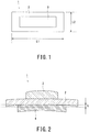
- Fig. 1, Fig. 2 , and Fig. 3 illustrate an example of the silicon nitride circuit board according to the embodiment.
- Fig. 1 and Fig. 3 are top views
- Fig. 2 is a lateral cross sectional view.
- reference numeral 1 denotes the silicon nitride circuit board
- reference numeral 2 denotes the silicon nitride substrate
- reference numeral 3 denotes the metal plate on the front side
- a metal plate 4 denotes the metal plate on the rear side.
- Reference character L1 denotes a length of the silicon nitride substrate in a long-side direction (longitudinal width)
- reference character L2 denotes a length of the silicon nitride substrate in a short-side direction (transverse width)
- reference character L3 denotes a length of the silicon nitride substrate in a diagonal line direction
- reference character S denotes a warp amount of the silicon nitride substrate.
- a warp amount of the silicon nitride substrate in the long-side direction is denoted by S L1
- a warp amount of the silicon nitride substrate in the short-side direction is denoted by S L2 .
- a warp amount of the silicon nitride substrate in the diagonal line direction is denoted by S L3 , which is not illustrated.
- a method for measuring the warp amount S is as follows. First, a straight line is drawn from one of opposite edges of the silicon nitride substrate to another one. The warp amount S is determined as a distance at which the silicon nitride substrate is most away from the straight line.
- the warp amount S L1 in the long-side direction and the warp amount S L2 in the short-side direction both fall within a range from 0.01 to 1.0 mm.
- the silicon nitride circuit board according to the embodiment has given warp amounts in both of the long-side direction and the short-side direction.
- the silicon nitride circuit board does not bend, which will be described later.
- the term "to bend” used herein refers to the warp amount S increasing beyond 1.0 mm.
- the warp amounts of the silicon nitride substrate in the long-side direction and the short-side direction both preferably fall within a range from 0.1 to 1.0 mm.
- the warp amount S L3 of the silicon nitride substrate in the diagonal line direction preferably falls within a range of 0.1 ⁇ S L3 ⁇ 1.5 mm.
- the warp amount S L3 in the diagonal line direction more preferably falls within a range of 0.2 ⁇ S L3 ⁇ 0.7 mm.
- the leadframe is attached mainly for the purpose of continuity of the semiconductor element. Therefore, the leadframe is often extended to an outside of the silicon nitride circuit board.
- the heat sink and the cooling fin are attached on the rear side of the silicon nitride circuit board.
- the heat sink and the cooling fin are attached regularly on the rear side.
- the leadframe is attached to a spot where a continuity is intended. Therefore, the leadframe is not always disposed regularly. Setting the warp amount S L3 in the diagonal line direction at 0.1 to 1.5 mm makes it possible to set the warp amount of the silicon nitride substrate in an electronic component module at less than 0.1 mm (0 mm included) even when the leadframe is disposed irregularly.
- a silicon nitride circuit board having a warp amount S L3 set within a range of 0.1 ⁇ S L3 ⁇ 1.5 mm is suitable for those to which leadframe are attached.
- the term "to dispose regularly” refers to dispositions of left-right symmetry.
- the longitudinal width L1 of the silicon nitride substrate is preferably 10 to 200 mm.
- the transverse width L2 of the silicon nitride substrate is preferably 10 to 200 mm. If the longitudinal width (L1) or the transverse width (L2) is short, being shorter than 10 mm, a footprint (mounting area) of a semiconductor element on the metal plate on the front side becomes small, and flexibility of design is decreased. In addition, it becomes difficult to form an area in which a bulging-out region of an attachment layer to be described later is provided. On the other hand, if the longitudinal width (L1) or the transverse width (L2) is long, being longer than 200 mm, it becomes difficult to control the warp amount (S) so that the warp amount (S) falls within a given range.
- a ratio (S L1/ S L2 ) between the warp amount (S L1 ) in the long-side direction and the warp amount (S L2 ) in the short-side direction preferably falls within a range from 1.2 to 20.0.
- the ratio (S L1/ S L2 ) more preferably falls within a range from 1.2 to 6.0.
- the ratio (S L1/ S L2 ) falling within the range from 1.2 to 20.0 indicates that the warp amounts in the long-side direction and the short-side direction are close to each other.
- the metal plate is preferably attached (bonded) to the silicon nitride substrate through an attachment layer (bonding layer) containing an active metal.
- the active metal refers to one, or two or more of elements selected from Ti (titanium), Zr (zirconium), Hf (hafnium), Nb (niobium), and Al (aluminum). Among these elements, Ti is preferably used, as mentioned before.
- the attachment layer containing the active metal is preferably one in which use is made of an active metal brazing material that contains 40 to 80% by mass of Ag, 20 to 60% by mass of Cu, 0.1 to 5% by mass of Ti, 20% by mass or less (0 included) of Sn, and 20% by mass or less (0 included) of In.
- the attachment is made by interposing an active metal brazing material layer between the silicon nitride substrate and the metal plate and performing heat treatment. After the attachment, the active metal in the attachment layer is preferably mainly made of an active metal nitride.
- the attachment layer preferably bulges out from edge portion of the metal plate.
- a bulging-out amount of the attachment layer bulging out from the edge portion of the metal plate is preferably 30 to 300 ⁇ m.
- Fig. 4 illustrates an example of a cross-sectional view of the silicon nitride circuit board in which the attachment layer includes a bulging-out portion.
- reference numeral 1 denotes the silicon nitride circuit board
- reference numeral 5 denotes the bulging-out portion of the attachment layer.
- Reference character W denotes the bulging-out amount of the attachment layer.
- the bulging-out portion 5 may climb up on a side surface of the metal plate. The provision of the bulging-out portion enables mitigation of thermal stress on the metal plate and the silicon nitride substrate.
- the bulging-out amount W preferably falls within a range from 50 to 300 ⁇ m, further a range from 50 to 200 ⁇ m.
- FIG. 8 illustrates an example of a lateral cross section of the metal plate of the silicon nitride circuit board according to the embodiment.
- reference numeral 2 denotes the silicon nitride substrate
- reference numeral 3 denotes the metal plate
- reference numeral 5 denotes the bulging-out portion of the attachment layer.
- a straight line is drawn from a point of 1/2 thickness of the metal plate 3 to the edge portion of the metal plate.
- An angle ⁇ between the straight line and the horizontal line being 60° or smaller indicates a shape of the side surface of the metal plate extending in a direction toward the silicon nitride substrate side. This shape enables mitigation of thermal stress on the metal plate and the silicon nitride substrate. Therefore, the angle ⁇ between the straight line and the horizontal line is preferably set to 60° or smaller, further 45° or smaller.
- the TCT (thermal cycle test) property can be improved even when the thickness of the metal plate is increased, or the difference in thickness between the metal plates on the front and rear sides (
- a bulging-out amount W less than 30 ⁇ m results in an insufficient effect of providing the bulging-out portion.
- a large bulging-out amount W exceeding 300 ⁇ m not only results in a failure to obtain an additional effect but also becomes a cause of an increase in cost. Therefore, the bulging-out amount W is preferably 30 to 300 ⁇ m, further 50 to 200 ⁇ m.
- the angle ⁇ is preferably set to 60° or smaller, further 45° or smaller. This configuration enables the mitigation of the thermal stress, thereby to improve the TCT property.
- the metal plate on the rear side is preferably larger in dimension than the longitudinal width (L1) and the transverse width (L2) of the silicon nitride substrate.
- Fig. 5 and Fig. 6 illustrate an example of the silicon nitride circuit board that has a structure in which the metal plate on the rear side is larger than the silicon nitride substrate.
- Fig. 5 is a lateral cross sectional view
- Fig. 6 is a top view.
- reference numeral 1 denotes the silicon nitride circuit board
- reference numeral 2 denotes the silicon nitride substrate
- reference numeral 3 denotes the metal plate on the front side
- reference numeral 4 denotes the metal plate on the rear side.
- Such a structure facilitates increasing the thickness t2 of the metal plate on the rear side. It is possible to establish a relation: t2 - t1 ⁇ 0.3 mm, further t2 - t1 ⁇ 0.8 mm. In addition, the thickness t2 of the metal plate on the rear side can be increased to be 1.0 mm or larger.
- Adopting the structure in which the metal plate on the rear side is larger than the silicon nitride substrate allows an efficient emission (radiation) of heat of an electronic component mounted on the metal plate on the front side. In general, the heat generated from the electronic component performs 45° diffusion (or 45° heat dissipation). Adopting the structure in which the metal plate on the rear side is larger than the silicon nitride substrate allows the 45° diffusion to proceed smoothly.
- the metal plate on the front side is a circuit plate
- the metal plate on the rear side is a heat dissipation plate
- (a volume of the metal plate on the rear side / a volume of the metal plate on the front side) ⁇ 2 is established.
- a volume of the heat dissipation plate (the metal plate on the rear side) is twice or more as large as a volume of the circuit plate (the metal plate on the front side).
- Examples of a method for increasing the volume include one to increase the thickness of the metal plate on the rear side, and one to increase longitudinal and transverse sizes of the metal plate on the rear side.
- a control of volume ratio between the metal plates on the front and rear sides is also effective in control of the warp amounts.
- H represents heat transfer path
- k thermal conductivity
- A heat dissipation area.
- the thermal conductivity (k) and the heat dissipation area (A) of the silicon nitride circuit board By increasing the thickness of the metal plate or increasing a size of the metal plate, it is possible to increase the thermal conductivity (k) and the heat dissipation area (A) of the silicon nitride circuit board. Consequently, the thermal resistance (Rth) can be decreased.
- the difference in thickness between the metal plates on the front side and the rear side is provided so that
- By increasing the thickness of the metal plate on the front side it is possible to given an additional current-carrying capacity.
- By increasing the thickness of the metal plate on the rear side it is possible to provide a broad emission path of heat, allowing an improved heat dissipation property.
- the silicon nitride substrate has warp amounts of 0.01 to 1.0 mm in the long-side direction and the short-side direction. Provision of the given warp amounts allows an improved TCT property even when the difference in thickness is large, being 0.30 mm or larger.
- Fig. 7 illustrates an example of the silicon nitride circuit board in which a plurality of metal plates are attached on the front side.
- reference numeral 1 denotes the silicon nitride circuit board
- reference numeral 2 denotes the silicon nitride substrate
- reference numeral 3 denotes the metal plates on the front side
- reference numeral 4 denotes the metal plate on the rear side.
- Fig. 7 is a configuration example in which two metal plates are arranged on the front side of the substrate.
- both of the metal plates are to satisfy the relation of
- a silicon nitride circuit board such as the one above is suitable for an electronic component module on which an electronic component is mounted.
- the electronic component include semiconductor elements and thermistors. Since the silicon nitride circuit board according to the embodiment has a decreased thermal resistance, the silicon nitride circuit board is suitable for a semiconductor element having a high junction temperature. An SiC device has a high junction temperature being 150°C or higher. In other words, the circuit board according to the present invention is suitable for an electronic component module on which a SiC device is mounted.
- a leadframe To the metal plate on the front side or the metal plate on the rear side, at least one of a leadframe, a heat sink, and a cooling fin having a thickness of 0.4 mm or larger is preferably attached.
- Fig. 9 illustrates an example of the electronic component module on which a leadframe is attached.
- Fig. 10 illustrates an example of the electronic component module on which a heat sink is attached.
- Fig. 11 illustrates an example of the electronic component module on which a cooling fin is attached.
- reference numeral 1 denotes the silicon nitride circuit board
- reference numeral 6 denotes the electronic component module
- reference numeral 7 denotes electronic components
- reference numeral 8 denotes the leadframe
- reference numeral 9 denotes the heat sink
- reference numeral 10 denotes the cooling fin.
- Fig. 9 illustrates the electronic component module in which the electronic components 7 and the leadframe 8 are connected to the metal plate 3 on the front side.
- the leadframe 8 preferably has a thickness of 0.4 mm or larger.
- Examples of the leadframe include a metal plate such as a copper plate.
- the thickness of the leadframe has any upper limit, which is however preferably 5 mm or smaller.
- Adopting such a structure enables a structure that dispenses with wire bonding. By not adopting a wire bonding structure, it is possible to effectively prevent a wire from being broken in performing resin sealing by a transfer molding method.
- an electronic component module is disposed in a heated mold.
- the electronic component module is disposed in a space called a cavity.
- the mold is made up of upper and lower molds as a set, defining the cavity.
- a resin tablet (resin in a hardened form) is charged into a space called a pot.
- the resin tablet charged into the pot starts to melt gradually and is charged into the cavity.
- With the resin in a liquid state a space around an electronic component is filled.
- the filling resin is hardened, the electronic component is brought into a molded state.
- the transfer molding method allows a molding process to be performed on a lot of electronic component modules by increasing a size of a mold and thus is a resin sealing method excellent in volume productivity (mass productivity).
- the transfer molding method is a manufacturing method in which a wire is likely to deform or to be broken. Therefore, by adopting the structure dispensing with wire bonding, it is possible to eliminate a break failure or a deformation failure of a wire in performing resin sealing by a transfer molding method.
- Fig. 10 illustrates the electronic component module in which a heat sink 9 is attached to the metal plate on the rear side.
- the heat sink 9 preferably has a thickness of 0.4 mm or larger.
- the heat sink is made up of a metal plate such as a copper plate.
- the upper limit of the thickness of the heat sink is not particularly limited, but the thickness is preferably 10 mm or smaller.
- Fig. 11 illustrates the electronic component module in which a cooling fin 10 is attached to the metal plate 4 on the rear side. While the heat sink 9 is in a plate shape, the cooling fin is in a comb shape.
- the comb shape may be in various protrusion shapes such as a groove shape and a pin shape. By adopting the comb shape, a heat dissipation area of the cooling fin can be increased.
- the thickness of the cooling fin does not have any particular upper limit, but is however preferably 20 mm or smaller.
- the leadframe the heat sink, and the cooling fin
- one may be attached, or two may be attached.
- two there are a combination of the leadframe and the heat sink, and a combination of the leadframe and the cooling fin.
- the warp amounts of the silicon nitride substrate in the long-side direction and the short-side direction both can be set at less than 0.1 mm (0 mm included).
- the attachment increases warp amounts of a silicon nitride circuit board.
- the silicon nitride circuit board according to the embodiment has given warp amounts, it is possible to mitigate a stress occurring when a thick leadframe or the like is attached. Therefore, the warp amounts of the silicon nitride substrate in the long-side direction and the short-side direction both can be decreased to less than 0.1 mm (0 mm included) when the electronic component module is formed.
- the electronic component module decreases the warp amounts of the silicon nitride substrate of the electronic component module facilitates resin sealing.
- the electronic component module according to the embodiment is suitable for a structure on which resin sealing is performed.
- the electronic component module is one to which a heat dissipating member such as a leadframe, a heat sink, and a cooling fin is attached, the electronic component module exerts an excellent TCT property. Even when a TCT (thermal cycle test) is actually conducted 600 cycles with 1 cycle of the TCT including -45°C ⁇ 30 min ⁇ room temperature (25°C) ⁇ 10 min ⁇ 150°C ⁇ 30 min ⁇ room temperature (25°C) ⁇ 10 min, no peeling occurs on the metal plate, and no crack occurs on the silicon nitride substrate. Therefore, the electronic component module exerts an excellent durability even when a SiC device, which has a high junction temperature, is used as an electronic component.
- a SiC device which has a high junction temperature
- the producing method for the silicon nitride circuit board according to the embodiment does not have any limit, and is any method as long as the silicon nitride circuit board has the structure mentioned before.
- examples of a method to efficiently obtain the silicon nitride circuit board include the following method.
- a silicon nitride substrate is prepared.
- the silicon nitride substrate is to be one having a three-point flexural strength of 500 MPa or higher.
- the silicon nitride substrate preferably has a fracture toughness value of 6.0 MPa ⁇ m 1/2 or higher.
- the silicon nitride substrate preferably has a thermal conductivity of 50 W/m ⁇ K or higher.
- the thermal conductivity is preferably 50 W/m ⁇ K or higher, further 80 W/m ⁇ K or higher.
- the silicon nitride substrate preferably has a thickness of 0.1 mm or larger and 0.70 mm or smaller. Further, a thickness reduction down to 0.33 mm or smaller and 0.26 mm or smaller is preferably performed.
- the warp amount S L1 in the long-side direction and the warp amount S L2 in the short-side direction are both supposed to be less than 0.1 mm.
- metal plates are prepared.
- the metal plates are preferably one selected from copper plates, copper alloy plates, Al plates, and Al alloy plates.
- the thicknesses of the metal plates are set so as to satisfy the relation
- an active metal brazing material is used.
- the active metal is supposed to contain one selected from Ti (titanium), Zr (zirconium), Hf (hafnium), and Nb (niobium).
- Ti is the most preferable.
- Components other than the active metal may include Ag, Cu, In, and Sn.
- the active metal brazing material one that contains 40 to 80% by mass of Ag, 20 to 60% by mass of Cu, 0.1 to 10% by mass of Ti, 20% by mass or less (0 included) of Sn, and 20% by mass or less (0 included) of In.
- the metal plates are Al plates or Al alloy plates
- Al aluminum
- a component other than the active metal include Si (silicon).
- an active metal brazing material in this case use is made of a brazing material that contains 0.01 to 10% by mass of Si, and Al as the remainder.
- the side surface of the metal plate may be worked in advance so that, when a straight line is drawn from a point of 1/2 thickness of the metal plate to an edge portion of the metal plate on a silicon nitride substrate side, an angle between the straight line and a horizontal line is 60° or smaller.
- the metal plate may be treated by etching treatment after the attachment so that, when a straight line is drawn from a point of 1/2 thickness of the metal plate to an edge portion of the metal plate on a silicon nitride substrate side, an angle between the straight line and the horizontal line is 60° or smaller.
- a resin binder is added to the active metal brazing material, whereby an active metal brazing material paste is prepared.
- the active metal brazing material paste is applied to the silicon nitride substrate, whereby an active metal brazing material paste layer is formed.
- the metal plate is disposed on the active metal brazing material paste layer.
- the active metal brazing material paste layer is provided as one that is slightly larger than a size of the metal plate in the longitudinal and transverse directions.
- An application thickness of the active metal brazing material paste layer preferably falls within a range from 10 to 40 ⁇ m. A thickness of the active metal brazing material paste layer less than 10 ⁇ m leads to a risk that a sufficient attachment strength (bonding strength) is not obtained.
- the thickness of the active metal brazing material paste layer preferably falls within a range from 10 to 40 ⁇ m, further 15 to 25 ⁇ m.
- a heating temperature preferably falls within a range from 600 to 900°C.
- an attachment temperature preferably falls within a range from 750 to 900°C.
- the attachment temperature preferably falls within a range from 600 to 750°C.
- the heating step is preferably performed in a vacuum atmosphere.
- a degree of vacuum is preferably 1 ⁇ 10 -2 Pa or lower, further 4 ⁇ 10 -3 Pa or lower. By performing the heating step in the vacuum atmosphere, it is possible to effectively prevent the copper plate or the active metal brazing material from being oxidized or nitrided.
- a cooling rate after the heating step is preferably set at 80°C/h or lower. By setting the cooling rate at a low rate, it is possible to mitigate thermal stress in the heating step.
- a step of attaching one or two of a leadframe, a heat sink, and a cooling fin is performed.
- the leadframe, the heat sink, and the cooling fin are preferably those having thicknesses of 0.4 mm or larger.
- the attachment of a heat dissipating member such as the leadframe, the heat sink, and the cooling fin is performed using solder.
- an electronic component is mounted on the metal plate on the front side.
- the electronic component may include semiconductor elements and thermistors.
- the mounting of the electronic component is preferably performed using solder.
- the attachment of the heat dissipating member such as the leadframe and the attachment of the electronic component may be performed at a same time in a same step or may be performed in different steps.
- a resin sealing step is performed.
- the resin sealing step is preferably performed by a transfer molding method.
- the transfer molding method is a method excellent in mass productivity.
- the silicon nitride circuit board according to the embodiment allows the warp amounts to be decreased even when the resin sealing is performed by the transfer molding method.
- a substrate having a thickness of 0.32 mm, a long-side direction length (L1) of 50 mm, a short-side direction length (L2) of 35 mm was prepared.
- the silicon nitride substrate had a three-point flexural strength of 600 MPa, a thermal conductivity of 90 W/m ⁇ K, and a fracture toughness value of 6.5 MPa ⁇ m 1/2 .
- metal plates copper plates were prepared.
- an active metal brazing material a brazing material containing Ag (60 wt%), Cu (30 wt%), In (8 wt%), and Ti (2 wt%) was prepared.
- the brazing material and a resin binder were mixed together, whereby an active metal brazing material paste was prepared.
- the active metal brazing material paste was applied, the copper plates were disposed, and the heating step was performed in a vacuum atmosphere, at 1 ⁇ 10 -3 Pa or lower, at 780 to 830°C.
- a cooling rate after the heating step was set at 50 to 70°C/h for Examples and at 300 to 400°C/h for Comparative Examples.
- Example 1 40 ⁇ 25 ⁇ 0.3 40 ⁇ 30 ⁇ 0.6 60 50
- Example 2 40 ⁇ 25 ⁇ 0.3 40 ⁇ 30 ⁇ 1.0 40 70
- Example 3 40 ⁇ 25 ⁇ 0.3 40 ⁇ 30 ⁇ 2.0 50
- Example 4 30 ⁇ 30 ⁇ 0.8 40 ⁇ 30 ⁇ 3.0 60 100
- Example 5 35 ⁇ 30 ⁇ 0.4 60 ⁇ 45 ⁇ 5.0 45 120
- Example 6 20 ⁇ 20 ⁇ 0.3.
- the warp amount S L1 in the long-side direction, the warp amount S L2 in the short-side direction, the warp amount S L3 in the diagonal line direction, and a direction of a warp were measured.
- the measurement of the warp amount was performed by drawing a straight line from one of opposite edges of the silicon nitride substrate to another one, as shown in Fig. 2 , and determining the warp amount as a distance at which the silicon nitride substrate is most away from the straight line. Results of the measurement are shown in Table 2 below. [Table 2] Sample No.
- Example 1 0.33 0.15 2.2 0.27 Convex toward Rear Side Example 2 0.8 0.5 1.6 0.7 Convex toward Front Side Example 3 0.7 0.6 1.2 0.55 Convex toward Front Side Example 4 1.0 0.5 2.0 0.9 Convex toward Rear Side Example 5 0.8 0.6 1.3 0.7 Convex toward Rear Side Example 6 0.6 0.1 6.0 0.5 Convex toward Rear Side Example 7 0.55 0.4 1.4 0.45 Convex toward Rear Side Comparative Example 1 0.00 0.00 - - - Comparative Example 2 0.25 0.25 1.0 0.20 Convex toward Rear Side Comparative Example 3 0.4 0.3 1.3 0.3 Convex toward Rear Side
- the silicon nitride circuit boards in Examples had warp amounts intended as an objective.
- substrates shown in Table 3 were prepared.
- warp amounts of the substrates warp amounts in the long-side direction were 0.02 mm or smaller, and warp amounts in the short-side direction were 0.02 mm or smaller.
- the step of attaching metal plates was the same as that in Example 1. [Table 3] Sample No.
- Example 8 Sizes of Substarte (Length ⁇ Width ⁇ Thickness mm) Three-Point Flexural Strength (MPa) Thermal Conductivity (W/m ⁇ K) Fracture Toughness Value (MPa ⁇ m 1/2 )
- Example 8 200 ⁇ 100 ⁇ 0.32 700 50 7.2
- Example 9 100 ⁇ 80 ⁇ 0.32 650 60 6.0
- Example 10 30 ⁇ 20 ⁇ 0.25 650 90 6.3
- Example 11 60 ⁇ 40 ⁇ 0.25 550 60 6.5
- Example 12 55 ⁇ 50 ⁇ 0.25 600 90 6.8
- Example 13 70 ⁇ 50 ⁇ 0.25 620 90 6.8
- Example 14 60 ⁇ 40 ⁇ 0.20 670 95 6.7
- Example 15 55 ⁇ 40 ⁇ 0.50 600 90 6.8
- Example 16 55 ⁇ 30 ⁇ 0.635 600 90 6.8
- Example 17 50 ⁇ 40 ⁇ 0.635 650 90 6.6
- the warp amount S L1 in the long-side direction, the warp amount S L2 in the short-side direction, the warp amount S L3 in the diagonal line direction, and a direction of a warp were measured.
- the measurement of the warp amount was performed by drawing a straight line from one of opposite edges of the silicon nitride substrate to another one, as shown in Fig. 2 , and determining the warp amount as a distance at which the substrate is most away from the straight line. Results of the measurement are shown in Table 5 below. [Table 5] Sample No.
- Example 8 0.9 0.65 1.4 1.0 Convex toward Rear Side Example 9 0.7 0.2 3.5 0.7 Convex toward Rear Side Example 10 0.3 0.1 3.0 0.2 Convex toward Rear Side Example 11 0.4 0.15 2.7 0.35 Convex toward Front Side Example 12 0.5 0.2 2.5 0.5 Convex toward Rear Side Example 13 0.85 0.65 1.3 0.9 Convex toward Rear Side Example 14 1.0 0.2 5.0 0.7 Convex toward Rear Side Example 15 0.9 0.1 9.0 0.7 Convex toward Rear Side Example 16 0.15 0.01 15.0 0.1 Convex toward Rear Side Example 17 0.9 0.05 18.0 0.95 Convex toward Rear Side
- TCT properties of the silicon nitride circuit boards and attachment strengths of the metal plates were measured.
- the TCT thermal cycle test
- 1 cycle thereof including -40°C ⁇ 30 min of retention ⁇ room temperature (25°C) ⁇ 10 min ⁇ 125°C ⁇ 30 min ⁇ room temperature (25°C) ⁇ 10 min, and presence/absence of peeling in the metal plate and occurrence of a crack in the silicon nitride substrate after 600 cycles were measured.
- the attachment strengths of the metal plates were measured in terms of peel strength. Results of the measurement are shown in Table 6. [Table 6] Sample No.
- a leadframe, a heat sink, a cooling fin were attached.
- the leadframe, the heat sink, and the cooling fin were all manufactured using copper plates.
- a semiconductor element was mounted on a front-side copper plate.
- the attachment of a heat dissipating member such as the leadframe, the heat sink, and the cooling fin, and the mounting of the semiconductor element were performed by solder attachment. Through these steps, electronic component modules were manufactured.
- TCT thermal cycle test
- 1 cycle including -45°C ⁇ 30 min ⁇ room temperature (25°C) ⁇ 10 min ⁇ 150°C ⁇ 30 min of retention ⁇ room temperature (25°C) ⁇ 10 min, presence/absence of peeling in the metal plate and occurrence of a crack after 600 cycles and 1000 cycles were performed were investigated. Results of the measurement and investigation are shown in Table 7 and Table 8 below. [Table 7] Sample No.
- the electronic component module in each Example exerted excellent TCT properties even when the heat dissipating member (the leadframe, the heat sink, and the cooling fin) having a thickness of 0.4 mm or larger was attached. In particular, even when the TCT test with a high-temperature region set at a higher temperature of 150°C was conducted, good results were also obtained.
- the electronic component module in each Example allows continuity using a leadframe, a structure dispensing with wire bonding can be adopted. Therefore, occurrence of a deformation failure or a break failure of a wire is avoided when the resin sealing is performed by the transfer molding method.
- the electronic component module according to the embodiment is suitable for a resin sealed structure by the transfer molding method.
Landscapes
- Engineering & Computer Science (AREA)
- Microelectronics & Electronic Packaging (AREA)
- Chemical & Material Sciences (AREA)
- Ceramic Engineering (AREA)
- Inorganic Chemistry (AREA)
- Cooling Or The Like Of Semiconductors Or Solid State Devices (AREA)
- Structures Or Materials For Encapsulating Or Coating Semiconductor Devices Or Solid State Devices (AREA)
Claims (13)
- Circuit imprimé en nitrure de silicium dans lequel des plaques en métal (3, 4) sont fixées sur des côtés avant et arrière d'un substrat en nitrure de silicium (2) ayant une résistance à la flexion en trois points de 500 MPa ou supérieure, dans lequelune épaisseur de la plaque en métal (3) sur le côté avant est indiquée par t1, et une épaisseur de la plaque en métal (4) sur le côté arrière est indiquée par t2, une relation numérique : |t1 - t2| ≥ 0,30 mm est satisfaite, et une déformation est formée dans le substrat en nitrure de silicium (2) de sorte que le substrat en nitrure de silicium (2) est convexe vers la plaque en métal (3, 4) sur un du côté avant ou du côté arrière ; etles quantités de déformation du substrat en nitrure de silicium (2) dans une direction côté long et une direction côté court se trouvent toutes deux dans un intervalle de 0,01 à 1,0 mm ;caractérisé en ce que(a) une quantité de déformation du substrat en nitrure de silicium (2) dans la direction côté long est indiquée par SL1, et une quantité de déformation du substrat en nitrure de silicium (2) dans la direction côté court est indiquée par SL2, un rapport (SL1/SL2) se trouve dans un intervalle de 1,2 à 20,0 ; et/ou(b) une longueur du substrat en nitrure de silicium (2) dans une direction de ligne diagonale est indiquée par L3, et une quantité de déformation dans la direction de ligne diagonale est indiquée par SL3, SL3 se trouve dans un intervalle de 0,1 mm ≤ SL3 ≤ 1,5 mm.
- Circuit imprimé en nitrure de silicium selon la revendication 1, dans lequel une largeur longitudinale (L1) du substrat en nitrure de silicium (2) se trouve dans un intervalle de 10 à 200 mm, et une largeur transversale (L2) du substrat en nitrure de silicium (2) se trouve dans un intervalle de 10 à 200 mm.
- Circuit imprimé en nitrure de silicium selon l'une quelconque de la revendication 1 ou revendication 2, dans lequel sur une surface latérale de la plaque en métal (3, 4), lorsqu'une ligne droite est tirée à partir d'un point de 1/2 épaisseur de la plaque en métal (3, 4) jusqu'à une portion de bord de la plaque en métal (3, 4) sur un côté de substrat en nitrure de silicium, la ligne droite et une surface du substrat en nitrure de silicium (2) forment un angle de 60° ou inférieur.
- Circuit imprimé en nitrure de silicium selon l'une quelconque de la revendication 1 à revendication 3, dans lequel chacune des plaques en métal (3, 4) est fixée au substrat en nitrure de silicium (2) par l'intermédiaire d'une couche de fixation contenant un métal actif intercalé entre celles-ci, et une quantité de saillie de la couche de fixation faisant saillie à partir d'une portion de bord de la plaque en métal (3, 4) est de 30 à 300 µm.
- Circuit imprimé en nitrure de silicium selon l'une quelconque de la revendication 1 à revendication 4, dans lequel la plaque en métal (4) sur le côté arrière est plus large qu'une largeur longitudinale (L1) et une largeur transversale (L2) du substrat en nitrure de silicium (2).
- Circuit imprimé en nitrure de silicium selon l'une quelconque de la revendication 1 à revendication 5, dans lequel le substrat en nitrure de silicium (2) présente une conductivité thermique de 50 W/m.K ou supérieure et une épaisseur de 0,70 mm ou inférieure.
- Circuit imprimé en nitrure de silicium selon l'une quelconque de la revendication 1 à revendication 6, dans lequel la plaque en métal (3) sur le côté avant est une plaque de circuit, la plaque en métal (4) sur le côté arrière est une plaque de dissipation de chaleur, et (un volume de la plaque en métal (4) sur le côté arrière/un volume de la plaque en métal (3) sur le côté avant) ≥ 2 est établi.
- Circuit imprimé en nitrure de silicium selon l'une quelconque de la revendication 1 à revendication 7, dans lequel il y a plusieurs plaques en métal (3, 4) fixées au côté avant.
- Module de constituant électronique comprenant le circuit imprimé en nitrure de silicium selon l'une quelconque de la revendication 1 à revendication 8, sur lequel un constituant électronique est monté.
- Module de constituant électronique selon la revendication 9, dans lequel au moins un d'un cadre conducteur (8), un puits thermique (9), et une ailette de refroidissement (10) ayant des épaisseurs de 0,4 mm ou supérieures est fixé à la plaque en métal (3) sur le côté avant ou la plaque en métal (4) sur le côté arrière.
- Module de constituant électronique selon la revendication 10 ou revendication 10, dans lequel au moins un d'un cadre conducteur (8), un puits thermique (9) et une ailette de refroidissement (10) présentant des épaisseurs de 0,4 mm ou supérieures est fixé à la plaque en métal (3) sur le côté avant ou la plaque en métal (4) sur le côté arrière, et une quantité de déformation du substrat en nitrure de silicium (2) dans la direction côté long et une quantité de déformation du substrat en nitrure de silicium (2) dans la direction côté court sont toutes deux inférieures à 0,1 mm (0 mm inclus).
- Module de constituant électronique selon l'une quelconque de la revendication 9 à revendication 11, dans lequel le module de constituant électronique est soumis à un scellement à la résine par un procédé de moulage par transfert.
- Module de constituant électronique selon l'une quelconque de la revendication 9 à revendication 12, dans lequel une continuité avec le constituant électronique se passe de câblage filaire.
Applications Claiming Priority (2)
| Application Number | Priority Date | Filing Date | Title |
|---|---|---|---|
| JP2015018515 | 2015-02-02 | ||
| PCT/JP2016/052190 WO2016125635A1 (fr) | 2015-02-02 | 2016-01-26 | Substrat de circuit de nitrure de silicium et module de composant électronique l'utilisant |
Publications (3)
| Publication Number | Publication Date |
|---|---|
| EP3255666A1 EP3255666A1 (fr) | 2017-12-13 |
| EP3255666A4 EP3255666A4 (fr) | 2018-09-26 |
| EP3255666B1 true EP3255666B1 (fr) | 2021-10-13 |
Family
ID=56563985
Family Applications (1)
| Application Number | Title | Priority Date | Filing Date |
|---|---|---|---|
| EP16746466.8A Active EP3255666B1 (fr) | 2015-02-02 | 2016-01-26 | Substrat de circuit de nitrure de silicium et module de composant électronique l'utilisant |
Country Status (4)
| Country | Link |
|---|---|
| US (2) | US10109555B2 (fr) |
| EP (1) | EP3255666B1 (fr) |
| JP (1) | JP6692299B2 (fr) |
| WO (1) | WO2016125635A1 (fr) |
Families Citing this family (8)
| Publication number | Priority date | Publication date | Assignee | Title |
|---|---|---|---|---|
| JP6829204B2 (ja) * | 2015-09-28 | 2021-02-10 | 株式会社東芝 | 窒化珪素回路基板およびそれを用いた半導体モジュール |
| JP6776953B2 (ja) * | 2017-03-07 | 2020-10-28 | 三菱マテリアル株式会社 | ヒートシンク付パワーモジュール用基板 |
| JPWO2019167942A1 (ja) * | 2018-02-27 | 2020-04-16 | 三菱マテリアル株式会社 | 絶縁回路基板 |
| WO2021095844A1 (fr) * | 2019-11-15 | 2021-05-20 | デンカ株式会社 | Substrat céramique, substrat composite, carte de circuit imprimé, procédé de production de substrat céramique, procédé de production de substrat composite, procédé de production de carte de circuit imprimé, et procédé pour la production d'une pluralité de cartes de circuit imprimé |
| JP7168795B2 (ja) * | 2019-11-15 | 2022-11-09 | デンカ株式会社 | セラミック基板、複合基板及び回路基板並びにセラミック基板の製造方法、複合基板の製造方法、回路基板の製造方法及び複数の回路基板の製造方法 |
| JP7363613B2 (ja) * | 2020-03-13 | 2023-10-18 | 三菱マテリアル株式会社 | ヒートシンク一体型絶縁回路基板 |
| WO2023120185A1 (fr) * | 2021-12-24 | 2023-06-29 | ローム株式会社 | Dispositif à semi-conducteur |
| JP7420204B2 (ja) * | 2022-02-25 | 2024-01-23 | 株式会社プロテリアル | 窒化珪素基板の評価方法、評価装置、及び評価システム |
Family Cites Families (15)
| Publication number | Priority date | Publication date | Assignee | Title |
|---|---|---|---|---|
| JP3949270B2 (ja) | 1998-05-13 | 2007-07-25 | 株式会社東芝 | セラミックス回路基板の製造方法 |
| US6613443B2 (en) | 2000-10-27 | 2003-09-02 | Kabushiki Kaisha Toshiba | Silicon nitride ceramic substrate, silicon nitride ceramic circuit board using the substrate, and method of manufacturing the substrate |
| JP3797905B2 (ja) | 2000-10-27 | 2006-07-19 | 株式会社東芝 | 窒化けい素セラミックス基板およびそれを用いた窒化けい素セラミックス回路基板並びにその製造方法 |
| JP2003168770A (ja) | 2001-12-04 | 2003-06-13 | Toshiba Corp | 窒化ケイ素回路基板 |
| JP4692708B2 (ja) * | 2002-03-15 | 2011-06-01 | Dowaメタルテック株式会社 | セラミックス回路基板およびパワーモジュール |
| JP3863067B2 (ja) | 2002-06-04 | 2006-12-27 | Dowaホールディングス株式会社 | 金属−セラミックス接合体の製造方法 |
| JP2007230791A (ja) | 2006-02-27 | 2007-09-13 | Kyocera Corp | セラミック回路基板およびその製造方法 |
| WO2007105361A1 (fr) | 2006-03-08 | 2007-09-20 | Kabushiki Kaisha Toshiba | Module de composant electronique |
| WO2009116439A1 (fr) | 2008-03-17 | 2009-09-24 | 三菱マテリアル株式会社 | Substrat pour module de puissance à dissipateur thermique et son procédé de fabrication, module de puissance à dissipateur thermique, et substrat pour module de puissance |
| JP5133960B2 (ja) | 2009-10-22 | 2013-01-30 | 電気化学工業株式会社 | 半導体搭載用回路基板及びその製造方法 |
| JP5047315B2 (ja) | 2010-01-26 | 2012-10-10 | 株式会社東芝 | セラミックス回路基板 |
| JP5218621B2 (ja) * | 2011-10-28 | 2013-06-26 | 日立金属株式会社 | 回路基板およびこれを用いた半導体モジュール |
| CN104011852B (zh) * | 2011-12-20 | 2016-12-21 | 株式会社东芝 | 陶瓷铜电路基板和使用了陶瓷铜电路基板的半导体装置 |
| JP2013229579A (ja) | 2012-03-30 | 2013-11-07 | Mitsubishi Materials Corp | パワーモジュール用基板、ヒートシンク付パワーモジュール用基板及びパワーモジュール |
| JP2014112732A (ja) | 2012-03-30 | 2014-06-19 | Mitsubishi Materials Corp | ヒートシンク付パワーモジュール用基板及びパワーモジュール |
-
2016
- 2016-01-26 EP EP16746466.8A patent/EP3255666B1/fr active Active
- 2016-01-26 JP JP2016573296A patent/JP6692299B2/ja active Active
- 2016-01-26 US US15/548,035 patent/US10109555B2/en active Active
- 2016-01-26 WO PCT/JP2016/052190 patent/WO2016125635A1/fr not_active Ceased
-
2018
- 2018-09-06 US US16/123,033 patent/US10366938B2/en active Active
Also Published As
| Publication number | Publication date |
|---|---|
| US10366938B2 (en) | 2019-07-30 |
| US20190006261A1 (en) | 2019-01-03 |
| EP3255666A1 (fr) | 2017-12-13 |
| JPWO2016125635A1 (ja) | 2017-11-09 |
| WO2016125635A1 (fr) | 2016-08-11 |
| US10109555B2 (en) | 2018-10-23 |
| JP6692299B2 (ja) | 2020-05-13 |
| EP3255666A4 (fr) | 2018-09-26 |
| US20180019182A1 (en) | 2018-01-18 |
Similar Documents
| Publication | Publication Date | Title |
|---|---|---|
| EP3255666B1 (fr) | Substrat de circuit de nitrure de silicium et module de composant électronique l'utilisant | |
| EP3358615B1 (fr) | Carte de circuit imprimé de nitrure de silicium et module semi-conducteur l'utilisant | |
| JP7451638B2 (ja) | セラミックス金属回路基板の製造方法および半導体装置の製造方法 | |
| EP2259308B1 (fr) | Substrat pour module de puissance a dissipateur thermique et son procede de fabrication, module de puissance a dissipateur thermique, et substrat pour module de puissance | |
| JP7048493B2 (ja) | セラミックス回路基板および半導体モジュール | |
| EP3537475B1 (fr) | Module de puissance et son procédé de fabrication | |
| JP2011124585A (ja) | セラミックス配線基板、その製造方法及び半導体モジュール | |
| JP5370460B2 (ja) | 半導体モジュール | |
| JP5218621B2 (ja) | 回路基板およびこれを用いた半導体モジュール | |
| JPWO2018021473A1 (ja) | 回路基板および半導体モジュール | |
| JP4893096B2 (ja) | 回路基板およびこれを用いた半導体モジュール | |
| JP5772088B2 (ja) | パワーモジュール用基板の製造方法及びパワーモジュール用基板 | |
| JP4893095B2 (ja) | 回路基板およびこれを用いた半導体モジュール | |
| US20140091444A1 (en) | Semiconductor unit and method for manufacturing the same |
Legal Events
| Date | Code | Title | Description |
|---|---|---|---|
| STAA | Information on the status of an ep patent application or granted ep patent |
Free format text: STATUS: THE INTERNATIONAL PUBLICATION HAS BEEN MADE |
|
| PUAI | Public reference made under article 153(3) epc to a published international application that has entered the european phase |
Free format text: ORIGINAL CODE: 0009012 |
|
| STAA | Information on the status of an ep patent application or granted ep patent |
Free format text: STATUS: REQUEST FOR EXAMINATION WAS MADE |
|
| 17P | Request for examination filed |
Effective date: 20170718 |
|
| AK | Designated contracting states |
Kind code of ref document: A1 Designated state(s): AL AT BE BG CH CY CZ DE DK EE ES FI FR GB GR HR HU IE IS IT LI LT LU LV MC MK MT NL NO PL PT RO RS SE SI SK SM TR |
|
| AX | Request for extension of the european patent |
Extension state: BA ME |
|
| DAV | Request for validation of the european patent (deleted) | ||
| DAX | Request for extension of the european patent (deleted) | ||
| A4 | Supplementary search report drawn up and despatched |
Effective date: 20180829 |
|
| RIC1 | Information provided on ipc code assigned before grant |
Ipc: H01L 23/373 20060101AFI20180823BHEP |
|
| REG | Reference to a national code |
Ref country code: DE Ref legal event code: R079 Ref document number: 602016064890 Country of ref document: DE Free format text: PREVIOUS MAIN CLASS: H01L0023360000 Ipc: H01L0023373000 |
|
| RIC1 | Information provided on ipc code assigned before grant |
Ipc: H05K 1/03 20060101ALI20210309BHEP Ipc: H05K 1/02 20060101ALI20210309BHEP Ipc: H01L 23/00 20060101ALI20210309BHEP Ipc: H01L 23/373 20060101AFI20210309BHEP |
|
| GRAP | Despatch of communication of intention to grant a patent |
Free format text: ORIGINAL CODE: EPIDOSNIGR1 |
|
| STAA | Information on the status of an ep patent application or granted ep patent |
Free format text: STATUS: GRANT OF PATENT IS INTENDED |
|
| INTG | Intention to grant announced |
Effective date: 20210430 |
|
| GRAS | Grant fee paid |
Free format text: ORIGINAL CODE: EPIDOSNIGR3 |
|
| GRAA | (expected) grant |
Free format text: ORIGINAL CODE: 0009210 |
|
| STAA | Information on the status of an ep patent application or granted ep patent |
Free format text: STATUS: THE PATENT HAS BEEN GRANTED |
|
| AK | Designated contracting states |
Kind code of ref document: B1 Designated state(s): AL AT BE BG CH CY CZ DE DK EE ES FI FR GB GR HR HU IE IS IT LI LT LU LV MC MK MT NL NO PL PT RO RS SE SI SK SM TR |
|
| REG | Reference to a national code |
Ref country code: GB Ref legal event code: FG4D |
|
| REG | Reference to a national code |
Ref country code: CH Ref legal event code: EP |
|
| REG | Reference to a national code |
Ref country code: DE Ref legal event code: R096 Ref document number: 602016064890 Country of ref document: DE |
|
| REG | Reference to a national code |
Ref country code: IE Ref legal event code: FG4D |
|
| REG | Reference to a national code |
Ref country code: AT Ref legal event code: REF Ref document number: 1438804 Country of ref document: AT Kind code of ref document: T Effective date: 20211115 |
|
| REG | Reference to a national code |
Ref country code: RO Ref legal event code: EPE |
|
| REG | Reference to a national code |
Ref country code: LT Ref legal event code: MG9D |
|
| REG | Reference to a national code |
Ref country code: NL Ref legal event code: MP Effective date: 20211013 |
|
| REG | Reference to a national code |
Ref country code: AT Ref legal event code: MK05 Ref document number: 1438804 Country of ref document: AT Kind code of ref document: T Effective date: 20211013 |
|
| PG25 | Lapsed in a contracting state [announced via postgrant information from national office to epo] |
Ref country code: RS Free format text: LAPSE BECAUSE OF FAILURE TO SUBMIT A TRANSLATION OF THE DESCRIPTION OR TO PAY THE FEE WITHIN THE PRESCRIBED TIME-LIMIT Effective date: 20211013 Ref country code: LT Free format text: LAPSE BECAUSE OF FAILURE TO SUBMIT A TRANSLATION OF THE DESCRIPTION OR TO PAY THE FEE WITHIN THE PRESCRIBED TIME-LIMIT Effective date: 20211013 Ref country code: FI Free format text: LAPSE BECAUSE OF FAILURE TO SUBMIT A TRANSLATION OF THE DESCRIPTION OR TO PAY THE FEE WITHIN THE PRESCRIBED TIME-LIMIT Effective date: 20211013 Ref country code: BG Free format text: LAPSE BECAUSE OF FAILURE TO SUBMIT A TRANSLATION OF THE DESCRIPTION OR TO PAY THE FEE WITHIN THE PRESCRIBED TIME-LIMIT Effective date: 20220113 Ref country code: AT Free format text: LAPSE BECAUSE OF FAILURE TO SUBMIT A TRANSLATION OF THE DESCRIPTION OR TO PAY THE FEE WITHIN THE PRESCRIBED TIME-LIMIT Effective date: 20211013 |
|
| PG25 | Lapsed in a contracting state [announced via postgrant information from national office to epo] |
Ref country code: IS Free format text: LAPSE BECAUSE OF FAILURE TO SUBMIT A TRANSLATION OF THE DESCRIPTION OR TO PAY THE FEE WITHIN THE PRESCRIBED TIME-LIMIT Effective date: 20220213 Ref country code: SE Free format text: LAPSE BECAUSE OF FAILURE TO SUBMIT A TRANSLATION OF THE DESCRIPTION OR TO PAY THE FEE WITHIN THE PRESCRIBED TIME-LIMIT Effective date: 20211013 Ref country code: PT Free format text: LAPSE BECAUSE OF FAILURE TO SUBMIT A TRANSLATION OF THE DESCRIPTION OR TO PAY THE FEE WITHIN THE PRESCRIBED TIME-LIMIT Effective date: 20220214 Ref country code: PL Free format text: LAPSE BECAUSE OF FAILURE TO SUBMIT A TRANSLATION OF THE DESCRIPTION OR TO PAY THE FEE WITHIN THE PRESCRIBED TIME-LIMIT Effective date: 20211013 Ref country code: NO Free format text: LAPSE BECAUSE OF FAILURE TO SUBMIT A TRANSLATION OF THE DESCRIPTION OR TO PAY THE FEE WITHIN THE PRESCRIBED TIME-LIMIT Effective date: 20220113 Ref country code: NL Free format text: LAPSE BECAUSE OF FAILURE TO SUBMIT A TRANSLATION OF THE DESCRIPTION OR TO PAY THE FEE WITHIN THE PRESCRIBED TIME-LIMIT Effective date: 20211013 Ref country code: LV Free format text: LAPSE BECAUSE OF FAILURE TO SUBMIT A TRANSLATION OF THE DESCRIPTION OR TO PAY THE FEE WITHIN THE PRESCRIBED TIME-LIMIT Effective date: 20211013 Ref country code: HR Free format text: LAPSE BECAUSE OF FAILURE TO SUBMIT A TRANSLATION OF THE DESCRIPTION OR TO PAY THE FEE WITHIN THE PRESCRIBED TIME-LIMIT Effective date: 20211013 Ref country code: GR Free format text: LAPSE BECAUSE OF FAILURE TO SUBMIT A TRANSLATION OF THE DESCRIPTION OR TO PAY THE FEE WITHIN THE PRESCRIBED TIME-LIMIT Effective date: 20220114 Ref country code: ES Free format text: LAPSE BECAUSE OF FAILURE TO SUBMIT A TRANSLATION OF THE DESCRIPTION OR TO PAY THE FEE WITHIN THE PRESCRIBED TIME-LIMIT Effective date: 20211013 |
|
| REG | Reference to a national code |
Ref country code: DE Ref legal event code: R097 Ref document number: 602016064890 Country of ref document: DE |
|
| PG25 | Lapsed in a contracting state [announced via postgrant information from national office to epo] |
Ref country code: SM Free format text: LAPSE BECAUSE OF FAILURE TO SUBMIT A TRANSLATION OF THE DESCRIPTION OR TO PAY THE FEE WITHIN THE PRESCRIBED TIME-LIMIT Effective date: 20211013 Ref country code: SK Free format text: LAPSE BECAUSE OF FAILURE TO SUBMIT A TRANSLATION OF THE DESCRIPTION OR TO PAY THE FEE WITHIN THE PRESCRIBED TIME-LIMIT Effective date: 20211013 Ref country code: EE Free format text: LAPSE BECAUSE OF FAILURE TO SUBMIT A TRANSLATION OF THE DESCRIPTION OR TO PAY THE FEE WITHIN THE PRESCRIBED TIME-LIMIT Effective date: 20211013 Ref country code: DK Free format text: LAPSE BECAUSE OF FAILURE TO SUBMIT A TRANSLATION OF THE DESCRIPTION OR TO PAY THE FEE WITHIN THE PRESCRIBED TIME-LIMIT Effective date: 20211013 Ref country code: CZ Free format text: LAPSE BECAUSE OF FAILURE TO SUBMIT A TRANSLATION OF THE DESCRIPTION OR TO PAY THE FEE WITHIN THE PRESCRIBED TIME-LIMIT Effective date: 20211013 |
|
| PLBE | No opposition filed within time limit |
Free format text: ORIGINAL CODE: 0009261 |
|
| STAA | Information on the status of an ep patent application or granted ep patent |
Free format text: STATUS: NO OPPOSITION FILED WITHIN TIME LIMIT |
|
| PG25 | Lapsed in a contracting state [announced via postgrant information from national office to epo] |
Ref country code: MC Free format text: LAPSE BECAUSE OF FAILURE TO SUBMIT A TRANSLATION OF THE DESCRIPTION OR TO PAY THE FEE WITHIN THE PRESCRIBED TIME-LIMIT Effective date: 20211013 |
|
| REG | Reference to a national code |
Ref country code: CH Ref legal event code: PL |
|
| 26N | No opposition filed |
Effective date: 20220714 |
|
| REG | Reference to a national code |
Ref country code: BE Ref legal event code: MM Effective date: 20220131 |
|
| PG25 | Lapsed in a contracting state [announced via postgrant information from national office to epo] |
Ref country code: LU Free format text: LAPSE BECAUSE OF NON-PAYMENT OF DUE FEES Effective date: 20220126 Ref country code: AL Free format text: LAPSE BECAUSE OF FAILURE TO SUBMIT A TRANSLATION OF THE DESCRIPTION OR TO PAY THE FEE WITHIN THE PRESCRIBED TIME-LIMIT Effective date: 20211013 |
|
| PG25 | Lapsed in a contracting state [announced via postgrant information from national office to epo] |
Ref country code: SI Free format text: LAPSE BECAUSE OF FAILURE TO SUBMIT A TRANSLATION OF THE DESCRIPTION OR TO PAY THE FEE WITHIN THE PRESCRIBED TIME-LIMIT Effective date: 20211013 Ref country code: BE Free format text: LAPSE BECAUSE OF NON-PAYMENT OF DUE FEES Effective date: 20220131 |
|
| PG25 | Lapsed in a contracting state [announced via postgrant information from national office to epo] |
Ref country code: LI Free format text: LAPSE BECAUSE OF NON-PAYMENT OF DUE FEES Effective date: 20220131 Ref country code: CH Free format text: LAPSE BECAUSE OF NON-PAYMENT OF DUE FEES Effective date: 20220131 |
|
| PG25 | Lapsed in a contracting state [announced via postgrant information from national office to epo] |
Ref country code: IE Free format text: LAPSE BECAUSE OF NON-PAYMENT OF DUE FEES Effective date: 20220126 |
|
| PG25 | Lapsed in a contracting state [announced via postgrant information from national office to epo] |
Ref country code: IT Free format text: LAPSE BECAUSE OF FAILURE TO SUBMIT A TRANSLATION OF THE DESCRIPTION OR TO PAY THE FEE WITHIN THE PRESCRIBED TIME-LIMIT Effective date: 20211013 |
|
| PG25 | Lapsed in a contracting state [announced via postgrant information from national office to epo] |
Ref country code: HU Free format text: LAPSE BECAUSE OF FAILURE TO SUBMIT A TRANSLATION OF THE DESCRIPTION OR TO PAY THE FEE WITHIN THE PRESCRIBED TIME-LIMIT; INVALID AB INITIO Effective date: 20160126 |
|
| PG25 | Lapsed in a contracting state [announced via postgrant information from national office to epo] |
Ref country code: MK Free format text: LAPSE BECAUSE OF FAILURE TO SUBMIT A TRANSLATION OF THE DESCRIPTION OR TO PAY THE FEE WITHIN THE PRESCRIBED TIME-LIMIT Effective date: 20211013 Ref country code: CY Free format text: LAPSE BECAUSE OF FAILURE TO SUBMIT A TRANSLATION OF THE DESCRIPTION OR TO PAY THE FEE WITHIN THE PRESCRIBED TIME-LIMIT Effective date: 20211013 |
|
| PG25 | Lapsed in a contracting state [announced via postgrant information from national office to epo] |
Ref country code: TR Free format text: LAPSE BECAUSE OF FAILURE TO SUBMIT A TRANSLATION OF THE DESCRIPTION OR TO PAY THE FEE WITHIN THE PRESCRIBED TIME-LIMIT Effective date: 20211013 |
|
| PG25 | Lapsed in a contracting state [announced via postgrant information from national office to epo] |
Ref country code: MT Free format text: LAPSE BECAUSE OF FAILURE TO SUBMIT A TRANSLATION OF THE DESCRIPTION OR TO PAY THE FEE WITHIN THE PRESCRIBED TIME-LIMIT Effective date: 20211013 |
|
| REG | Reference to a national code |
Ref country code: DE Ref legal event code: R079 Ref document number: 602016064890 Country of ref document: DE Free format text: PREVIOUS MAIN CLASS: H01L0023373000 Ipc: H10W0040250000 |
|
| PGFP | Annual fee paid to national office [announced via postgrant information from national office to epo] |
Ref country code: GB Payment date: 20251204 Year of fee payment: 11 |
|
| PGFP | Annual fee paid to national office [announced via postgrant information from national office to epo] |
Ref country code: FR Payment date: 20251128 Year of fee payment: 11 |
|
| PGFP | Annual fee paid to national office [announced via postgrant information from national office to epo] |
Ref country code: RO Payment date: 20251224 Year of fee payment: 11 |
|
| REG | Reference to a national code |
Ref country code: DE Ref legal event code: R081 Ref document number: 602016064890 Country of ref document: DE Owner name: NITERRA MATERIALS CO., LTD., YOKOHAMA-SHI, JP Free format text: FORMER OWNERS: KABUSHIKI KAISHA TOSHIBA, MINATO-KU, TOKYO, JP; TOSHIBA MATERIALS CO., LTD., YOKOHAMA-SHI, KANAGAWA, JP |
|
| PGFP | Annual fee paid to national office [announced via postgrant information from national office to epo] |
Ref country code: DE Payment date: 20251203 Year of fee payment: 11 |