EP3329361B1 - Commande de nombre de bits d'opérande de vecteur - Google Patents
Commande de nombre de bits d'opérande de vecteur Download PDFInfo
- Publication number
- EP3329361B1 EP3329361B1 EP16731312.1A EP16731312A EP3329361B1 EP 3329361 B1 EP3329361 B1 EP 3329361B1 EP 16731312 A EP16731312 A EP 16731312A EP 3329361 B1 EP3329361 B1 EP 3329361B1
- Authority
- EP
- European Patent Office
- Prior art keywords
- exception level
- level state
- vector operand
- vector
- bit size
- Prior art date
- Legal status (The legal status is an assumption and is not a legal conclusion. Google has not performed a legal analysis and makes no representation as to the accuracy of the status listed.)
- Active
Links
Images


Classifications
-
- G—PHYSICS
- G06—COMPUTING OR CALCULATING; COUNTING
- G06F—ELECTRIC DIGITAL DATA PROCESSING
- G06F9/00—Arrangements for program control, e.g. control units
- G06F9/06—Arrangements for program control, e.g. control units using stored programs, i.e. using an internal store of processing equipment to receive or retain programs
- G06F9/30—Arrangements for executing machine instructions, e.g. instruction decode
- G06F9/30003—Arrangements for executing specific machine instructions
- G06F9/30007—Arrangements for executing specific machine instructions to perform operations on data operands
- G06F9/30036—Instructions to perform operations on packed data, e.g. vector, tile or matrix operations
- G06F9/30038—Instructions to perform operations on packed data, e.g. vector, tile or matrix operations using a mask
-
- G—PHYSICS
- G06—COMPUTING OR CALCULATING; COUNTING
- G06F—ELECTRIC DIGITAL DATA PROCESSING
- G06F15/00—Digital computers in general; Data processing equipment in general
- G06F15/76—Architectures of general purpose stored program computers
- G06F15/80—Architectures of general purpose stored program computers comprising an array of processing units with common control, e.g. single instruction multiple data processors
- G06F15/8007—Architectures of general purpose stored program computers comprising an array of processing units with common control, e.g. single instruction multiple data processors single instruction multiple data [SIMD] multiprocessors
-
- G—PHYSICS
- G06—COMPUTING OR CALCULATING; COUNTING
- G06F—ELECTRIC DIGITAL DATA PROCESSING
- G06F15/00—Digital computers in general; Data processing equipment in general
- G06F15/76—Architectures of general purpose stored program computers
- G06F15/80—Architectures of general purpose stored program computers comprising an array of processing units with common control, e.g. single instruction multiple data processors
- G06F15/8053—Vector processors
-
- G—PHYSICS
- G06—COMPUTING OR CALCULATING; COUNTING
- G06F—ELECTRIC DIGITAL DATA PROCESSING
- G06F9/00—Arrangements for program control, e.g. control units
- G06F9/06—Arrangements for program control, e.g. control units using stored programs, i.e. using an internal store of processing equipment to receive or retain programs
- G06F9/30—Arrangements for executing machine instructions, e.g. instruction decode
- G06F9/30003—Arrangements for executing specific machine instructions
- G06F9/30007—Arrangements for executing specific machine instructions to perform operations on data operands
- G06F9/30036—Instructions to perform operations on packed data, e.g. vector, tile or matrix operations
-
- G—PHYSICS
- G06—COMPUTING OR CALCULATING; COUNTING
- G06F—ELECTRIC DIGITAL DATA PROCESSING
- G06F9/00—Arrangements for program control, e.g. control units
- G06F9/06—Arrangements for program control, e.g. control units using stored programs, i.e. using an internal store of processing equipment to receive or retain programs
- G06F9/30—Arrangements for executing machine instructions, e.g. instruction decode
- G06F9/30145—Instruction analysis, e.g. decoding, instruction word fields
- G06F9/30149—Instruction analysis, e.g. decoding, instruction word fields of variable length instructions
-
- G—PHYSICS
- G06—COMPUTING OR CALCULATING; COUNTING
- G06F—ELECTRIC DIGITAL DATA PROCESSING
- G06F9/00—Arrangements for program control, e.g. control units
- G06F9/06—Arrangements for program control, e.g. control units using stored programs, i.e. using an internal store of processing equipment to receive or retain programs
- G06F9/30—Arrangements for executing machine instructions, e.g. instruction decode
- G06F9/30181—Instruction operation extension or modification
- G06F9/30189—Instruction operation extension or modification according to execution mode, e.g. mode flag
-
- G—PHYSICS
- G06—COMPUTING OR CALCULATING; COUNTING
- G06F—ELECTRIC DIGITAL DATA PROCESSING
- G06F9/00—Arrangements for program control, e.g. control units
- G06F9/06—Arrangements for program control, e.g. control units using stored programs, i.e. using an internal store of processing equipment to receive or retain programs
- G06F9/30—Arrangements for executing machine instructions, e.g. instruction decode
- G06F9/30181—Instruction operation extension or modification
- G06F9/30192—Instruction operation extension or modification according to data descriptor, e.g. dynamic data typing
-
- G—PHYSICS
- G06—COMPUTING OR CALCULATING; COUNTING
- G06F—ELECTRIC DIGITAL DATA PROCESSING
- G06F9/00—Arrangements for program control, e.g. control units
- G06F9/06—Arrangements for program control, e.g. control units using stored programs, i.e. using an internal store of processing equipment to receive or retain programs
- G06F9/30—Arrangements for executing machine instructions, e.g. instruction decode
- G06F9/38—Concurrent instruction execution, e.g. pipeline or look ahead
- G06F9/3861—Recovery, e.g. branch miss-prediction, exception handling
Definitions
- This disclosure relates to the field of data processing systems. More particularly, this disclosure relates to data processing systems supporting vector processing operations.
- the vector operand bit size is defined as part of the architecture of the data processing system, e. g. the architecture defines that the vector operand bit size will be some specific fixed value, such as 256 bits, 512 bits, 1024 bits etc.
- GB 2478731 A discloses a data processing system with processing circuitry and a bank of 64-bit registers.
- An instruction decoder decodes arithmetic and logical instructions specifying arithmetic and logical operations to be performed upon operands stored in the 64-bit registers.
- the logical instructions have an operand size field specifying the size of the operands, i. e. 64-bit or 32-bit operands.
- Each 64-bit register stores either a single 64-bit operand or a single 32-bit operand. For a given arithmetic or logical instruction either all of the operands are 64-bit operands or all are 32-bit operands.
- the circuitry may have a plurality of hierarchy of exception levels such that, if a switch is made to a lower exception level, then a check is made as to size of the previous write to the register being used. If the write was a 64-bit write, then the upper 32-bits are flushed so as to avoid data leakage from the higher exception level.
- At least some embodiments of the disclosure provide a method of processing data, comprising:
- Figure 1 schematically illustrates a data processing system 2 comprising a processor 4 and a memory 6 storing data 8 and program instructions 10.
- the processor 4 includes instruction fetch circuitry 12 that fetches program instructions 10 from the memory 6 and passes these to decoder circuitry 14 where they are decoded to generate control signals 16 that control the operation of the processor 4. More particularly, the control signals 16 control processing circuitry 18 to perform processing operations specified by the decoded program instructions.
- the processing circuitry 18 is coupled to vector register circuitry 20 for storing vector operands having a vector operand bit size and containing a plurality of vector elements.
- System configuration registers 22 are also coupled to the processing circuitry 18 and serve to store configuration values which may be programmed under software control by the processing circuitry 18 and which serve to configure the behaviour of the processing circuitry 18, such as the vector operand bit size used for vector processing instructions and the constraint of vector operand bit size in accordance with programmable limit values (PLVs).
- PLVs programmable limit values
- the first example vector operand 24 is a general purpose vector operand, such as may be used as a source operand or a destination operand when executing a vector program instruction (e.g. a vector arithmetic instruction, a vector logic instruction, etc.).
- a vector program instruction e.g. a vector arithmetic instruction, a vector logic instruction, etc.
- the general purpose vector operand 24 is illustrated as having a vector operand bit size of 512 bits and as containing eight vector elements each having a vector element bit size of 64 bits.
- the vector elements are denoted as a 0 to a 7 .
- Figure 2 also illustrates another example form of vector operand, namely a vector predicate operand 26.
- This may be a vector predicate operand associated with a vector processing operation being performed upon the general purpose vector operand 24.
- the vector predicate operand 26 contains a plurality of predicate values p 0 to p 7 which control the execution of an associated vector program instruction in respect of the corresponding vector elements within the vector operand manipulated by that vector program instruction.
- predicate values may switch on or switch off the vector processing associated with respective vector elements within a general purpose vector operand.
- the vector predicate operand has 64 bits and each predicate value is eight bits in length.
- the data processing system 2 of Figure 1 is implemented with a particular implementation of the vector register circuitry 22 used to store the vector operands 24, 26.
- different physical implementations using the processor architecture of the present disclosure may provide vector operands with differing implementation limited maximum bit sizes.
- a complex implementation aimed at high processing speed may provide vector operands with a large bit size, such as 1024 bits.
- an implementation of a processor aimed at providing a lower energy consumption during operation may support a smaller maximum vector operand bit size such as 128 bits. It is desirable that software written to execute on the processor architecture of the data processing system 2 should be able to be used without any (or significant) modification dependant upon the implementation limited vector operand bit size of the particular processor 4 being used to execute that software.
- particular software may have been tested/validated to work with particular vector operand bit sizes and the software may itself wish to constrain the vector operand bit sizes used in its execution to be different from (less than) the implementation maximum vector operand bit size.
- exception level states e.g. privilege levels
- Figure 3 schematically illustrates programmable limit values associated with different exception level states for a particular implementation of the processor 4.
- the implementation limited maximum operand bit size is 512.
- the processor 4 supports execution in four different exception level states, namely EL0, EL1, EL2 and EL3. These exception level states are arranged in a hierarchy of exception level states extending from a bottom exception level state EL0 to a top exception level state EL3.
- Each of the exception level states, other than the bottom exception level state has a programmable limit value (PLV x ) associated therewith.
- the bottom exception level state EL0 may also have a programmable limit value (PLV 0 ) associated therewith.
- exception level state EL1 has a programmable limit value of 384 bits
- exception level state EL2 has a programmable limit value of 256 bits
- exception level EL3 has a programmable limit level of 512 bits.
- These programmable limit values indicate the maximum vector operand bit size to be used to execute vector program instructions executing at the exception level state concerned and at all exception level states below the exception level state concerned.
- the programmable limit value associated with an exception level state imposes a limit upon the vector operand size for program instructions executing at its own exception level and further imposes this limit upon program instructions executing at lower exception levels within the hierarchy of exception level states.
- a hypervisor executing at exception level state EL2 may support a maximum vector operand bit size of 256 and this limit will be imposed upon operating system software executing at exception level EL1 and application software executing at exception level EL0, even though these other instance of software may themselves be capable of using a greater vector operand bit size as may be specified by their own programmable limit value, e.g. the operating system at exception level state EL1.
- the vector operand bit size employed is controlled (and used by the processing circuitry 18) so as to perform processing with the vector operand bit size governed by a limit value of the currently selected exception level state and any (all) programmable limit value set for an exception level state closer to the top exception level state within the hierarchy than the currently selected selection level state (which itself may or may not be programmable).
- the bottom exception level state (in this example embodiment) does not have an associated programmable limit value, but is subject to the programmable limit values of all of the other exception level states, which are closer to the top of the hierarchy than the bottom exception level state.
- a vector program instruction will normally use a vector operand bit size which has a largest value permitted for a vector operand bit size dependant instruction being executed. This provides increased levels of parallel operation.
- the decoder circuitry 14 and processing circuitry 18 support a permitted operand bit size querying instruction.
- This permitted vector operand bit size querying instruction serves to return a vector operand bit size indicating value constrained by exception level states closer to the top exception level state within the hierarchy than the selected exception level state in which the processing circuitry 18 executes the permitted vector operand bit size querying instruction.
- a permitted vector operand bit size querying instruction executed in exception level state EL0 corresponding to the bottom exception level state used by an application program, will return a permitted vector operand bit size indicating value of 256 which is constrained by the programmable limit value for exception level state EL2 of 256, even though the exception level state EL0 (in this example embodiment) has no associated limit value and the limit value associated with the operating system executing at exception level EL1 is a higher value of 384.
- the permitted vector operand bit size indicating value that is returned is dependant upon the programmable limit values associated with higher exception level states but not any programmable limit value associated with the selected exception state at which the permitted vector operand bit size querying instruction is itself executed.
- execution of a permitted vector operand bit size querying instruction at exception level state EL2 returns a permitted vector operand bit size indicating value of 512 as this is the programmable limit value associated with the exception level state EL3 even though the programmable limit value associated with exception level state EL2 itself is 256.
- the permitted vector operand bit size querying instruction allows software executing at a particular exception level state to determine a maximum vector operand bit size it may use, such as to set its own programmable limit value or to modify some other aspect of its behaviour.
- Figure 4 is a generalised version of the specific example given in Figure 3 .
- the vector operand bit size used for a vector operand bit size dependant instruction at a given exception level is determined as the minimum indicated by the programmable limit value of that exception level state itself as well has other programmable limit values closer to the top exception level state within the hierarchy.
- exception level EL0 in this example embodiment, this does not itself have a programmable limit value and accordingly its vector operand bit size is determined as the minimum indicated by all the programmable limit values of the higher exception level states within the hierarchy.
- the top exception level state EL(N-1) has a vector operand bit size used for its vector operand bit size dependant instructions that is specified by its own programmable limit value PLV (n-1) .
- the returned vector operand bit size indicating value in the case of the generalised example of Figure 4 , this is given by the minimum indicated by all programmable limit values associated with higher exception level states within the hierarchy compared to the exception level state at which the permitted vector operand bit size querying instruction is itself executed.
- the returned permitted vector operand bit size indicating value is the implementation limited vector operand bit size of the particularly implementation of the processor 4 (and vector register circuitry 20).
- Figure 5 schematically illustrates an example of the form of the system registers 22 which may be used to control the above described behaviour.
- These system registers 22 include an identification register ZIDR_EL1 together with a plurality of exception level configuration registers ZCR_EL x
- the decoder circuitry 14 is responsive to the permitted vector operand bit size querying instruction and the current exception level state (thereby rendering the instruction context sensitive) to read the identification register ZIDR_EL1 .
- the value returned from such a register read is the permitted vector operand bit size indicating value that is determined as described above in relation to the Figure 3 and 4 .
- execution of the permitted vector operand bit size querying instruction may appear to the programmer as reading an identification system register
- the result may be drawn from other sources including the plurality of exception level configuration registers ZCR_EL x and the implementation limited maximum operand bit size.
- the effect of execution of the vector operand bit size querying instruction is to return the least significant bits of the identification register ZIDR_EL1. This has a value corresponding to the maximum permitted vector operand bit size indicating value as previously discussed. Which of the exception level configuration registers ZCR_EL x this return value depends upon is controlled by the exception level state in which the permitted vector operand bit size querying instruction is executed.
- an attempt the read the identification register ZIDR_EL1 may not return a value and the instruction may then instead be treated as an undefined instruction triggering an undefined instruction exception.
- the exception level configuration registers ZCR_EL x associated with respective exception level states other than the bottom level exception level states are used to store programmable limit values PLV x that are set by writes to these exception level configuration registers.
- a system register read or write instruction to an exception level configuration registers ZCR_EL x executed at a given exception level state is permitted to read or write the exception level configuration register of its own exception level state, and any lower exception level state (closer to the bottom exception level state) within the hierarchy of exception level states.
- An attempt to read or write an exception level configuration register ZCR_EL x of a higher exception level state results in undefined instruction behaviour.
- the programmable limit values may in this example embodiment may be 4-bit values and are used to indicate vector operand bit size by incrementing by 1 and multiplying by 128. It will be apparent that other mappings between the programmable limit values and the vector operand bit sizes they specify may also be employed, e.g. specify the vector operand size as a power of 2.
- Figure 6A is a flow diagram schematically illustrating the execution of a context sensitive vector operand bit size dependant instruction.
- processing waits until a vector operand bit size dependant instruction is received by the decoder 14.
- the decoder 14 then generates control signals 16 to control the processing circuitry 18 and other elements within the processor to read the currently selected exception level state programmable limit value and all higher exception level state programmable limit values at step 30.
- Step 32 determines the minimum of these read values.
- Step 34 performs the processing specified by the vector operand bit size dependant instruction (such as an arithmetic operation, a logical operation or some other operation) using as the vector operand bit size the minimum value determined at step 32.
- FIG. 6B is a flow diagram schematically illustrating the operation of a context sensitive permitted vector operand bit size querying instruction.
- processing waits until a permitted vector operand bit size querying instruction is received by the decoder circuitry 14.
- This permitted vector operand bit size querying instruction may be, for example, a read of the identification register ZIDR_EL1.
- processing proceeds to step 38 where a read is made of the programmable limit values set for all higher exception level states (and as appropriate the implementation limited maximum vector operand bit size).
- Step 40 determines the minimum of the read values from step 38.
- Step 42 returns the minimum of the read values as the maximum permitted vector operand bit size (permitted vector operand bit size indicating value). Processing then terminates.
- Figure 7 is a flow diagram schematically illustrating the behaviour of the processor 4 when writing a programmable limit value PLV to one of the system configuration registers 22.
- the programmable limit value which may be set for a given exception level state is limited by the programmable limit values set for higher exception level states, and is also limited by the constraints of the particular implementation of the processor 4.
- a particular implementation of the processor 4 may support vector operand bit sizes of 512, 256 and 128, but not support vector operand bit sizes of 384.
- a system register write instruction to one of the exception level configuration registers ZCR_EL x is seeking to define a programmable limit value corresponding to a vector operand bit size of 384, this may be permitted by programmable limit values higher in the exception level state hierarchy, but is not permitted by the hardware implementation of the processor 4.
- the programmable limit value which is stored within the exception level configuration register ZCR_EL x in response to the system register write instruction is rounded to the next lowest hardware supported vector operand bit size.
- an attempted write of a programmable limited value corresponding to 384 in the above example may be permitted by the programmable limit values of higher exception level states, but is not permitted by the hardware implementation, and accordingly the values stored is rounded to the next lowest supported vector operand size, namely 256.
- software executing at a particular exception level state may determine which vector operand bit sizes are and are not supported as a consequence of both programmable limits set by software at higher exception level state and limits set by the hardware implementation.
- processing waits until an instruction writing to an exception level configuration register ZCR_EL x is received by the decoder 14.
- Step 46 determines whether the specified programmable limit value being written is one supported by the hardware. Additional checks (not illustrated) are performed to ensure that the written value does not conflict with the programmable limit values of higher exception level states.
- step 48 serves to write the specified programmable limit value to the state configuration register concerned. If the programmable limit value to be written is determined by step 46 not to be supported by the hardware, then processing proceeds via step 50 whereby a rounded programmable limit value is instead written to the state configuration value having being rounded to the next lowest value that is supported by the hardware implementation concerned.
- Figure 8 schematically illustrates the behaviour of the processing system when the vector operand bit size is increased. It will be appreciated that by the use of the programmable limit values software may dynamically changed the vector operand bit size in use. Such changes can have significant operational consequences to the system and this is one reason why the bottom exception level state is not permitted to control its own vector operand bit size so as to avoid application programs which typically execute in this bottom exception level state, from producing undesired behaviour.
- a newly accessible portion 52 of a vector operand becomes available for use by vector processing instructions.
- the processing system 2 responds to such increases in vector operand bit size by zeroing the values within the newly accessible portion of the vector operand, or alternatively by ensuring that the values within the newly accessible portion have been preserved in a state that they had when the newly accessible portion was last available for use.
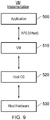
- Figure 9 illustrates a virtual machine implementation that may be used. Whilst the earlier described embodiments implement the present invention in terms of apparatus and methods for operating specific processing hardware supporting the techniques concerned, it is also possible to provide so-called virtual machine implementations of hardware devices. These virtual machine implementations run on a host processor 530 running a host operating system 520 supporting a virtual machine program 510. Typically, large powerful processors are required to provide virtual machine implementations which execute at a reasonable speed, but such an approach may be justified in certain circumstances, such as when there is a desire to run code native to another processor for compatibility or re-use reasons.
- the virtual machine program 510 provides an application program interface to an application program 500 which is the same as the application program interface which would be provided by the real hardware which is the device being modelled by the virtual machine program 510.
- the program instructions including the control of memory accesses described above, may be executed from within the application program 500 using the virtual machine program 510 to model their interaction with the virtual machine hardware.
Landscapes
- Engineering & Computer Science (AREA)
- Theoretical Computer Science (AREA)
- Software Systems (AREA)
- Physics & Mathematics (AREA)
- General Engineering & Computer Science (AREA)
- General Physics & Mathematics (AREA)
- Computer Hardware Design (AREA)
- Mathematical Physics (AREA)
- Computing Systems (AREA)
- Executing Machine-Instructions (AREA)
- Advance Control (AREA)
- Complex Calculations (AREA)
Claims (14)
- Appareil de traitement de données, comprenant :une circuiterie de traitement pour réaliser des opérations de traitement dans un état de niveau d'exception sélectionné d'une hiérarchie d'états de niveau d'exception s'étendant entre un état de niveau d'exception maximum et un état de niveau d'exception minimum ; etune circuiterie de décodage pour décoder des instructions de programme afin de générer des signaux de commande servant à commander la circuiterie de traitement pour réaliser lesdites opérations de traitement, lesdites opérations de traitement comportant des opérations de traitement vectoriel utilisant au moins un opérande de vecteur ; dans lequelladite circuiterie de décodage répond à une instruction de programme dépendant d'un nombre de bits d'opérande de vecteur exécutée dans ledit état de niveau d'exception sélectionné pour commander ladite circuiterie de traitement afin de réaliser des opérations de traitement vectoriel dépendant d'une valeur limite de nombre de bits d'opérande de vecteur dudit état de niveau d'exception sélectionné et d'au moins une valeur limite de nombre de bits d'opérande de vecteur programmable d'un état de niveau d'exception plus proche dudit état de niveau d'exception maximum dans ladite hiérarchie que ledit état de niveau d'exception sélectionné.
- Appareil selon la revendication 1, dans lequel ledit nombre de bits d'opérande de vecteur a la plus haute valeur permise par ladite valeur limite pour ledit état de niveau d'exception sélectionné et également permise par n'importe quelle valeur limite programmable réglée pour un état de niveau d'exception plus proche dudit état de niveau d'exception maximum dans ladite hiérarchie que ledit état de niveau d'exception sélectionné.
- Appareil selon l'une quelconque des revendications 1 et 2, dans lequel ladite circuiterie de décodage répond à une instruction d'interrogation du nombre de bits d'opérande de vecteur pour renvoyer une valeur d'indication du nombre de bits d'opérande de vecteur autorisé régie par n'importe quelle valeur limite programmable réglée pour un état de niveau d'exception plus proche dudit état de niveau d'exception maximum dans ladite hiérarchie que ledit état de niveau d'exception sélectionné.
- Appareil selon l'une quelconque des revendications 1, 2 et 3, comprenant une pluralité de registres de configuration de niveau d'exception stockant des valeurs limites programmables respectives pour ledit nombre de bits d'opérande de vecteur associées à des états de niveau d'exception correspondants dans ladite hiérarchie.
- Appareil selon la revendication 4, comprenant un registre de configuration de niveau d'exception respectif pour chaque état de niveau d'exception dans ladite hiérarchie à l'exclusion dudit état de niveau d'exception minimum.
- Appareil selon l'une quelconque des revendications 4 et 5, dans lequel ladite circuiterie de traitement est autorisée à accéder à un registre de configuration de niveau d'exception dudit état d'exception sélectionné et à n'importe quels registres de configuration de niveau d'exception d'états de niveau d'exception plus proches dudit état de niveau d'exception minimum dans ladite hiérarchie que ledit état de niveau d'exception sélectionné.
- Appareil selon la revendication 3, dans lequel ladite circuiterie de traitement est empêchée d'interroger ledit nombre de bits d'opérande de vecteur autorisé en utilisant ladite instruction d'interrogation du nombre de bits d'opérande de vecteur autorisé quand ladite circuiterie de traitement est dans ledit état de niveau d'exception minimum.
- Appareil selon l'une quelconque des revendications précédentes, dans lequel ladite circuiterie de traitement comprend une circuiterie d'enregistrement d'opérandes de vecteur pour stocker des opérandes de vecteur présentant jusqu'à un nombre de bits d'opérande de vecteur limité de mise en œuvre et dans lequel lesdites valeurs limites programmables commandent ladite circuiterie de traitement pour réaliser ladite instruction dépendant du nombre de bits d'opérande de vecteur en utilisant un nombre de bits d'opérande de vecteur égal ou inférieur audit nombre de bits d'opérande de vecteur limité de mise en œuvre.
- Appareil selon l'une quelconque des revendications précédentes, dans lequel ledit opérande de vecteur est l'un : d'un opérande de vecteur universel ; et d'un opérande de prédicat de vecteur spécifiant des valeurs de prédicats pour commander l'exécution d'une instruction de programme vectoriel.
- Appareil selon l'une quelconque des revendications précédentes, dans lequel ladite circuiterie de traitement répond à une tentative de réglage d'une valeur limite programmable à une valeur correspondant à un nombre de bits d'opérande de vecteur non pris en charge par ledit appareil pour régler ladite valeur limite programmable à un nombre de bits d'opérande de vecteur inférieur suivant qui est pris en charge par ledit appareil.
- Appareil selon l'une quelconque des revendications précédentes, dans lequel ladite circuiterie de traitement répond à une augmentation du nombre de bits d'opérande de vecteur, lors au moins d'un changement dudit de niveau d'exception sélectionné et d'un changement d'au moins une dite valeur limite programmable, pour fournir dans une partie nouvellement accessible dudit opérande de vecteur une de valeurs zéro ou de valeurs contenues dans ladite partie nouvellement accessible quand ladite partie nouvellement accessible était accessible la dernière fois.
- Appareil selon la revendication 3, dans lequel ladite instruction d'interrogation du nombre de bits d'opérande de vecteur autorisé est une instruction de lecture de registre système.
- Procédé de traitement de données, comprenant :la réalisation d'opérations de traitement avec une circuiterie de traitement dans un état de niveau d'exception sélectionné d'une hiérarchie d'états de niveau d'exception s'étendant entre un état de niveau d'exception maximum et un état de niveau d'exception minimum ; etle décodage d'instructions de programme pour générer des signaux de commande afin de commander ladite circuiterie de traitement pour réaliser lesdites opérations de traitement, lesdites opérations de traitement comportant des opérations de traitement vectoriel utilisant au moins un opérande de vecteur ; dans lequelen réponse au décodage d'une instruction de programme dépendant du nombre de bits d'opérande de vecteur exécutée dans ledit état de niveau d'exception sélectionné, la commande de ladite circuiterie de traitement pour réaliser des opérations de traitement vectoriel en fonction d'une valeur limite de nombre de bits d'opérande de vecteur dudit état de niveau d'exception sélectionné et d'au moins une valeur limite de taille d'opérande de vecteur programmable d'un état de niveau d'exception plus proche dudit état de niveau d'exception maximum dans ladite hiérarchie que ledit état de niveau d'exception sélectionné.
- Programme informatique mémorisé sur un support de mémorisation non transitoire qui, à son exécution, commande un ordinateur pour fournir un environnement d'exécution de machine virtuelle correspondant à l'appareil selon l'une quelconque des revendications 1 à 12.
Applications Claiming Priority (2)
| Application Number | Priority Date | Filing Date | Title |
|---|---|---|---|
| GB1513512.2A GB2540944B (en) | 2015-07-31 | 2015-07-31 | Vector operand bitsize control |
| PCT/GB2016/051857 WO2017021680A1 (fr) | 2015-07-31 | 2016-06-21 | Commande de nombre de bits d'opérande de vecteur |
Publications (2)
| Publication Number | Publication Date |
|---|---|
| EP3329361A1 EP3329361A1 (fr) | 2018-06-06 |
| EP3329361B1 true EP3329361B1 (fr) | 2020-08-05 |
Family
ID=54062957
Family Applications (1)
| Application Number | Title | Priority Date | Filing Date |
|---|---|---|---|
| EP16731312.1A Active EP3329361B1 (fr) | 2015-07-31 | 2016-06-21 | Commande de nombre de bits d'opérande de vecteur |
Country Status (9)
| Country | Link |
|---|---|
| US (1) | US10409602B2 (fr) |
| EP (1) | EP3329361B1 (fr) |
| JP (1) | JP6874262B2 (fr) |
| KR (1) | KR102581576B1 (fr) |
| CN (1) | CN107851015B (fr) |
| GB (1) | GB2540944B (fr) |
| IL (1) | IL256440B (fr) |
| TW (1) | TWI710956B (fr) |
| WO (1) | WO2017021680A1 (fr) |
Families Citing this family (6)
| Publication number | Priority date | Publication date | Assignee | Title |
|---|---|---|---|---|
| GB2540944B (en) * | 2015-07-31 | 2018-02-21 | Advanced Risc Mach Ltd | Vector operand bitsize control |
| GB2562102B (en) * | 2017-05-05 | 2019-09-04 | Advanced Risc Mach Ltd | An apparatus and method for managing use of capabilities |
| GB201907382D0 (en) * | 2019-05-24 | 2019-07-10 | Univ Southampton | Computer-implemented method for creating encoded data for use in a cognitive computing system, as well as cognitive processing unit and cognitive computing |
| US11917067B2 (en) * | 2019-12-28 | 2024-02-27 | Intel Corporation | Apparatuses, methods, and systems for instructions for usage restrictions cryptographically tied with data |
| GB2597708B (en) | 2020-07-30 | 2022-11-02 | Advanced Risc Mach Ltd | Vector processing |
| US20240220248A1 (en) * | 2022-12-29 | 2024-07-04 | Intel Corporation | Restricting vector length in a processor |
Family Cites Families (21)
| Publication number | Priority date | Publication date | Assignee | Title |
|---|---|---|---|---|
| US5513366A (en) * | 1994-09-28 | 1996-04-30 | International Business Machines Corporation | Method and system for dynamically reconfiguring a register file in a vector processor |
| DE19826826A1 (de) * | 1998-06-16 | 1999-07-15 | Siemens Ag | Verfahren zum Decodieren und Ausführen von Befehlen in einem RISC-Prozessor |
| US20030221086A1 (en) * | 2002-02-13 | 2003-11-27 | Simovich Slobodan A. | Configurable stream processor apparatus and methods |
| GB2474901B (en) | 2009-10-30 | 2015-01-07 | Advanced Risc Mach Ltd | Apparatus and method for performing multiply-accumulate operations |
| US8555034B2 (en) * | 2009-12-15 | 2013-10-08 | Oracle America, Inc. | Execution of variable width vector processing instructions |
| GB2478731B (en) * | 2010-03-15 | 2013-08-21 | Advanced Risc Mach Ltd | Operand size control |
| GB2478726B (en) * | 2010-03-15 | 2013-12-25 | Advanced Risc Mach Ltd | Mapping between registers used by multiple instruction sets |
| JP5720111B2 (ja) * | 2010-04-16 | 2015-05-20 | 富士通株式会社 | 情報処理装置 |
| US20110320765A1 (en) * | 2010-06-28 | 2011-12-29 | International Business Machines Corporation | Variable width vector instruction processor |
| CN107608716B (zh) * | 2011-04-01 | 2020-12-15 | 英特尔公司 | 向量友好指令格式及其执行 |
| GB2489914B (en) * | 2011-04-04 | 2019-12-18 | Advanced Risc Mach Ltd | A data processing apparatus and method for performing vector operations |
| CN103907089B (zh) * | 2011-04-07 | 2017-07-07 | 威盛电子股份有限公司 | 一种乱序执行微处理器中的有条件加载指令 |
| JP5673322B2 (ja) * | 2011-04-18 | 2015-02-18 | 富士通株式会社 | ベクトル処理装置、システムおよびベクトル処理装置の動作方法 |
| WO2013095611A1 (fr) * | 2011-12-23 | 2013-06-27 | Intel Corporation | Appareil et procédé pour effectuer une opération de permutation |
| WO2013101132A1 (fr) * | 2011-12-29 | 2013-07-04 | Intel Corporation | Processeurs ayant des interconnexions entièrement connectées partagées par des instructions de conflit vectoriel et des instructions de permutation |
| US9594724B2 (en) * | 2012-08-09 | 2017-03-14 | International Business Machines Corporation | Vector register file |
| US20140281418A1 (en) * | 2013-03-14 | 2014-09-18 | Shihjong J. Kuo | Multiple Data Element-To-Multiple Data Element Comparison Processors, Methods, Systems, and Instructions |
| US9348589B2 (en) * | 2013-03-19 | 2016-05-24 | Apple Inc. | Enhanced predicate registers having predicates corresponding to element widths |
| US9552209B2 (en) | 2013-12-27 | 2017-01-24 | Intel Corporation | Functional unit for instruction execution pipeline capable of shifting different chunks of a packed data operand by different amounts |
| US11544214B2 (en) * | 2015-02-02 | 2023-01-03 | Optimum Semiconductor Technologies, Inc. | Monolithic vector processor configured to operate on variable length vectors using a vector length register |
| GB2540944B (en) * | 2015-07-31 | 2018-02-21 | Advanced Risc Mach Ltd | Vector operand bitsize control |
-
2015
- 2015-07-31 GB GB1513512.2A patent/GB2540944B/en active Active
-
2016
- 2016-06-21 KR KR1020187003458A patent/KR102581576B1/ko active Active
- 2016-06-21 US US15/741,551 patent/US10409602B2/en active Active
- 2016-06-21 EP EP16731312.1A patent/EP3329361B1/fr active Active
- 2016-06-21 CN CN201680043311.3A patent/CN107851015B/zh active Active
- 2016-06-21 WO PCT/GB2016/051857 patent/WO2017021680A1/fr not_active Ceased
- 2016-06-21 JP JP2018503484A patent/JP6874262B2/ja active Active
- 2016-07-21 TW TW105122999A patent/TWI710956B/zh active
-
2017
- 2017-12-20 IL IL256440A patent/IL256440B/en active IP Right Grant
Non-Patent Citations (1)
| Title |
|---|
| None * |
Also Published As
| Publication number | Publication date |
|---|---|
| TWI710956B (zh) | 2020-11-21 |
| IL256440A (en) | 2018-02-28 |
| JP2018521421A (ja) | 2018-08-02 |
| US20180203699A1 (en) | 2018-07-19 |
| KR102581576B1 (ko) | 2023-09-22 |
| JP6874262B2 (ja) | 2021-05-19 |
| GB2540944B (en) | 2018-02-21 |
| CN107851015A (zh) | 2018-03-27 |
| IL256440B (en) | 2020-03-31 |
| WO2017021680A1 (fr) | 2017-02-09 |
| GB201513512D0 (en) | 2015-09-16 |
| TW201712535A (zh) | 2017-04-01 |
| US10409602B2 (en) | 2019-09-10 |
| EP3329361A1 (fr) | 2018-06-06 |
| GB2540944A (en) | 2017-02-08 |
| CN107851015B (zh) | 2022-04-26 |
| KR20180034471A (ko) | 2018-04-04 |
Similar Documents
| Publication | Publication Date | Title |
|---|---|---|
| US9804851B2 (en) | Operand size control | |
| EP3329361B1 (fr) | Commande de nombre de bits d'opérande de vecteur | |
| JP6807383B2 (ja) | 転送プレフィックス命令 | |
| JP5984865B2 (ja) | 命令エミュレーションプロセッサ、方法、およびシステム | |
| US8938605B2 (en) | Instruction cracking based on machine state | |
| GB2478726A (en) | Instruction decoder for a processor able to deal with N-bit length data and 2N-bit length data using a set of registers. | |
| JP2019504403A5 (fr) | ||
| WO1997050031A1 (fr) | Procede permettant d'accroitre le rendement d'instructions conditionnelles traduites en format binaire | |
| KR102590679B1 (ko) | 벡터 요소들 내부의 비트 값들의 시험 | |
| WO2012136975A1 (fr) | Appareil de traitement de données et procédé servant à effectuer des opérations vectorielles | |
| US11003447B2 (en) | Vector arithmetic and logical instructions performing operations on different first and second data element widths from corresponding first and second vector registers | |
| KR20130098303A (ko) | 정렬 제어 | |
| JP7377208B2 (ja) | データ処理 | |
| US12008371B2 (en) | Method and apparatus for efficient programmable instructions in computer systems |
Legal Events
| Date | Code | Title | Description |
|---|---|---|---|
| STAA | Information on the status of an ep patent application or granted ep patent |
Free format text: STATUS: THE INTERNATIONAL PUBLICATION HAS BEEN MADE |
|
| PUAI | Public reference made under article 153(3) epc to a published international application that has entered the european phase |
Free format text: ORIGINAL CODE: 0009012 |
|
| STAA | Information on the status of an ep patent application or granted ep patent |
Free format text: STATUS: REQUEST FOR EXAMINATION WAS MADE |
|
| 17P | Request for examination filed |
Effective date: 20180127 |
|
| AK | Designated contracting states |
Kind code of ref document: A1 Designated state(s): AL AT BE BG CH CY CZ DE DK EE ES FI FR GB GR HR HU IE IS IT LI LT LU LV MC MK MT NL NO PL PT RO RS SE SI SK SM TR |
|
| AX | Request for extension of the european patent |
Extension state: BA ME |
|
| DAV | Request for validation of the european patent (deleted) | ||
| DAX | Request for extension of the european patent (deleted) | ||
| STAA | Information on the status of an ep patent application or granted ep patent |
Free format text: STATUS: EXAMINATION IS IN PROGRESS |
|
| 17Q | First examination report despatched |
Effective date: 20190315 |
|
| GRAP | Despatch of communication of intention to grant a patent |
Free format text: ORIGINAL CODE: EPIDOSNIGR1 |
|
| STAA | Information on the status of an ep patent application or granted ep patent |
Free format text: STATUS: GRANT OF PATENT IS INTENDED |
|
| INTG | Intention to grant announced |
Effective date: 20200310 |
|
| GRAS | Grant fee paid |
Free format text: ORIGINAL CODE: EPIDOSNIGR3 |
|
| GRAA | (expected) grant |
Free format text: ORIGINAL CODE: 0009210 |
|
| STAA | Information on the status of an ep patent application or granted ep patent |
Free format text: STATUS: THE PATENT HAS BEEN GRANTED |
|
| AK | Designated contracting states |
Kind code of ref document: B1 Designated state(s): AL AT BE BG CH CY CZ DE DK EE ES FI FR GB GR HR HU IE IS IT LI LT LU LV MC MK MT NL NO PL PT RO RS SE SI SK SM TR |
|
| REG | Reference to a national code |
Ref country code: GB Ref legal event code: FG4D |
|
| REG | Reference to a national code |
Ref country code: CH Ref legal event code: EP |
|
| REG | Reference to a national code |
Ref country code: AT Ref legal event code: REF Ref document number: 1299664 Country of ref document: AT Kind code of ref document: T Effective date: 20200815 |
|
| REG | Reference to a national code |
Ref country code: DE Ref legal event code: R096 Ref document number: 602016041334 Country of ref document: DE |
|
| REG | Reference to a national code |
Ref country code: IE Ref legal event code: FG4D |
|
| REG | Reference to a national code |
Ref country code: LT Ref legal event code: MG4D |
|
| REG | Reference to a national code |
Ref country code: NL Ref legal event code: MP Effective date: 20200805 |
|
| REG | Reference to a national code |
Ref country code: AT Ref legal event code: MK05 Ref document number: 1299664 Country of ref document: AT Kind code of ref document: T Effective date: 20200805 |
|
| PG25 | Lapsed in a contracting state [announced via postgrant information from national office to epo] |
Ref country code: PT Free format text: LAPSE BECAUSE OF FAILURE TO SUBMIT A TRANSLATION OF THE DESCRIPTION OR TO PAY THE FEE WITHIN THE PRESCRIBED TIME-LIMIT Effective date: 20201207 Ref country code: GR Free format text: LAPSE BECAUSE OF FAILURE TO SUBMIT A TRANSLATION OF THE DESCRIPTION OR TO PAY THE FEE WITHIN THE PRESCRIBED TIME-LIMIT Effective date: 20201106 Ref country code: FI Free format text: LAPSE BECAUSE OF FAILURE TO SUBMIT A TRANSLATION OF THE DESCRIPTION OR TO PAY THE FEE WITHIN THE PRESCRIBED TIME-LIMIT Effective date: 20200805 Ref country code: SE Free format text: LAPSE BECAUSE OF FAILURE TO SUBMIT A TRANSLATION OF THE DESCRIPTION OR TO PAY THE FEE WITHIN THE PRESCRIBED TIME-LIMIT Effective date: 20200805 Ref country code: LT Free format text: LAPSE BECAUSE OF FAILURE TO SUBMIT A TRANSLATION OF THE DESCRIPTION OR TO PAY THE FEE WITHIN THE PRESCRIBED TIME-LIMIT Effective date: 20200805 Ref country code: HR Free format text: LAPSE BECAUSE OF FAILURE TO SUBMIT A TRANSLATION OF THE DESCRIPTION OR TO PAY THE FEE WITHIN THE PRESCRIBED TIME-LIMIT Effective date: 20200805 Ref country code: NO Free format text: LAPSE BECAUSE OF FAILURE TO SUBMIT A TRANSLATION OF THE DESCRIPTION OR TO PAY THE FEE WITHIN THE PRESCRIBED TIME-LIMIT Effective date: 20201105 Ref country code: ES Free format text: LAPSE BECAUSE OF FAILURE TO SUBMIT A TRANSLATION OF THE DESCRIPTION OR TO PAY THE FEE WITHIN THE PRESCRIBED TIME-LIMIT Effective date: 20200805 Ref country code: AT Free format text: LAPSE BECAUSE OF FAILURE TO SUBMIT A TRANSLATION OF THE DESCRIPTION OR TO PAY THE FEE WITHIN THE PRESCRIBED TIME-LIMIT Effective date: 20200805 Ref country code: BG Free format text: LAPSE BECAUSE OF FAILURE TO SUBMIT A TRANSLATION OF THE DESCRIPTION OR TO PAY THE FEE WITHIN THE PRESCRIBED TIME-LIMIT Effective date: 20201105 |
|
| PG25 | Lapsed in a contracting state [announced via postgrant information from national office to epo] |
Ref country code: NL Free format text: LAPSE BECAUSE OF FAILURE TO SUBMIT A TRANSLATION OF THE DESCRIPTION OR TO PAY THE FEE WITHIN THE PRESCRIBED TIME-LIMIT Effective date: 20200805 Ref country code: LV Free format text: LAPSE BECAUSE OF FAILURE TO SUBMIT A TRANSLATION OF THE DESCRIPTION OR TO PAY THE FEE WITHIN THE PRESCRIBED TIME-LIMIT Effective date: 20200805 Ref country code: RS Free format text: LAPSE BECAUSE OF FAILURE TO SUBMIT A TRANSLATION OF THE DESCRIPTION OR TO PAY THE FEE WITHIN THE PRESCRIBED TIME-LIMIT Effective date: 20200805 Ref country code: PL Free format text: LAPSE BECAUSE OF FAILURE TO SUBMIT A TRANSLATION OF THE DESCRIPTION OR TO PAY THE FEE WITHIN THE PRESCRIBED TIME-LIMIT Effective date: 20200805 Ref country code: IS Free format text: LAPSE BECAUSE OF FAILURE TO SUBMIT A TRANSLATION OF THE DESCRIPTION OR TO PAY THE FEE WITHIN THE PRESCRIBED TIME-LIMIT Effective date: 20201205 |
|
| PG25 | Lapsed in a contracting state [announced via postgrant information from national office to epo] |
Ref country code: EE Free format text: LAPSE BECAUSE OF FAILURE TO SUBMIT A TRANSLATION OF THE DESCRIPTION OR TO PAY THE FEE WITHIN THE PRESCRIBED TIME-LIMIT Effective date: 20200805 Ref country code: CZ Free format text: LAPSE BECAUSE OF FAILURE TO SUBMIT A TRANSLATION OF THE DESCRIPTION OR TO PAY THE FEE WITHIN THE PRESCRIBED TIME-LIMIT Effective date: 20200805 Ref country code: DK Free format text: LAPSE BECAUSE OF FAILURE TO SUBMIT A TRANSLATION OF THE DESCRIPTION OR TO PAY THE FEE WITHIN THE PRESCRIBED TIME-LIMIT Effective date: 20200805 Ref country code: SM Free format text: LAPSE BECAUSE OF FAILURE TO SUBMIT A TRANSLATION OF THE DESCRIPTION OR TO PAY THE FEE WITHIN THE PRESCRIBED TIME-LIMIT Effective date: 20200805 Ref country code: RO Free format text: LAPSE BECAUSE OF FAILURE TO SUBMIT A TRANSLATION OF THE DESCRIPTION OR TO PAY THE FEE WITHIN THE PRESCRIBED TIME-LIMIT Effective date: 20200805 |
|
| REG | Reference to a national code |
Ref country code: DE Ref legal event code: R097 Ref document number: 602016041334 Country of ref document: DE |
|
| PG25 | Lapsed in a contracting state [announced via postgrant information from national office to epo] |
Ref country code: AL Free format text: LAPSE BECAUSE OF FAILURE TO SUBMIT A TRANSLATION OF THE DESCRIPTION OR TO PAY THE FEE WITHIN THE PRESCRIBED TIME-LIMIT Effective date: 20200805 |
|
| PLBE | No opposition filed within time limit |
Free format text: ORIGINAL CODE: 0009261 |
|
| STAA | Information on the status of an ep patent application or granted ep patent |
Free format text: STATUS: NO OPPOSITION FILED WITHIN TIME LIMIT |
|
| PG25 | Lapsed in a contracting state [announced via postgrant information from national office to epo] |
Ref country code: SK Free format text: LAPSE BECAUSE OF FAILURE TO SUBMIT A TRANSLATION OF THE DESCRIPTION OR TO PAY THE FEE WITHIN THE PRESCRIBED TIME-LIMIT Effective date: 20200805 |
|
| 26N | No opposition filed |
Effective date: 20210507 |
|
| PG25 | Lapsed in a contracting state [announced via postgrant information from national office to epo] |
Ref country code: IT Free format text: LAPSE BECAUSE OF FAILURE TO SUBMIT A TRANSLATION OF THE DESCRIPTION OR TO PAY THE FEE WITHIN THE PRESCRIBED TIME-LIMIT Effective date: 20200805 |
|
| PG25 | Lapsed in a contracting state [announced via postgrant information from national office to epo] |
Ref country code: SI Free format text: LAPSE BECAUSE OF FAILURE TO SUBMIT A TRANSLATION OF THE DESCRIPTION OR TO PAY THE FEE WITHIN THE PRESCRIBED TIME-LIMIT Effective date: 20200805 |
|
| PG25 | Lapsed in a contracting state [announced via postgrant information from national office to epo] |
Ref country code: MC Free format text: LAPSE BECAUSE OF FAILURE TO SUBMIT A TRANSLATION OF THE DESCRIPTION OR TO PAY THE FEE WITHIN THE PRESCRIBED TIME-LIMIT Effective date: 20200805 |
|
| REG | Reference to a national code |
Ref country code: CH Ref legal event code: PL |
|
| REG | Reference to a national code |
Ref country code: BE Ref legal event code: MM Effective date: 20210630 |
|
| PG25 | Lapsed in a contracting state [announced via postgrant information from national office to epo] |
Ref country code: LU Free format text: LAPSE BECAUSE OF NON-PAYMENT OF DUE FEES Effective date: 20210621 |
|
| PG25 | Lapsed in a contracting state [announced via postgrant information from national office to epo] |
Ref country code: LI Free format text: LAPSE BECAUSE OF NON-PAYMENT OF DUE FEES Effective date: 20210630 Ref country code: IE Free format text: LAPSE BECAUSE OF NON-PAYMENT OF DUE FEES Effective date: 20210621 Ref country code: CH Free format text: LAPSE BECAUSE OF NON-PAYMENT OF DUE FEES Effective date: 20210630 |
|
| PG25 | Lapsed in a contracting state [announced via postgrant information from national office to epo] |
Ref country code: BE Free format text: LAPSE BECAUSE OF NON-PAYMENT OF DUE FEES Effective date: 20210630 |
|
| P01 | Opt-out of the competence of the unified patent court (upc) registered |
Effective date: 20230429 |
|
| PG25 | Lapsed in a contracting state [announced via postgrant information from national office to epo] |
Ref country code: CY Free format text: LAPSE BECAUSE OF FAILURE TO SUBMIT A TRANSLATION OF THE DESCRIPTION OR TO PAY THE FEE WITHIN THE PRESCRIBED TIME-LIMIT Effective date: 20200805 |
|
| PG25 | Lapsed in a contracting state [announced via postgrant information from national office to epo] |
Ref country code: HU Free format text: LAPSE BECAUSE OF FAILURE TO SUBMIT A TRANSLATION OF THE DESCRIPTION OR TO PAY THE FEE WITHIN THE PRESCRIBED TIME-LIMIT; INVALID AB INITIO Effective date: 20160621 |
|
| PG25 | Lapsed in a contracting state [announced via postgrant information from national office to epo] |
Ref country code: MK Free format text: LAPSE BECAUSE OF FAILURE TO SUBMIT A TRANSLATION OF THE DESCRIPTION OR TO PAY THE FEE WITHIN THE PRESCRIBED TIME-LIMIT Effective date: 20200805 |
|
| PG25 | Lapsed in a contracting state [announced via postgrant information from national office to epo] |
Ref country code: TR Free format text: LAPSE BECAUSE OF FAILURE TO SUBMIT A TRANSLATION OF THE DESCRIPTION OR TO PAY THE FEE WITHIN THE PRESCRIBED TIME-LIMIT Effective date: 20200805 |
|
| PG25 | Lapsed in a contracting state [announced via postgrant information from national office to epo] |
Ref country code: MT Free format text: LAPSE BECAUSE OF FAILURE TO SUBMIT A TRANSLATION OF THE DESCRIPTION OR TO PAY THE FEE WITHIN THE PRESCRIBED TIME-LIMIT Effective date: 20200805 |
|
| PGFP | Annual fee paid to national office [announced via postgrant information from national office to epo] |
Ref country code: DE Payment date: 20250520 Year of fee payment: 10 |
|
| PGFP | Annual fee paid to national office [announced via postgrant information from national office to epo] |
Ref country code: GB Payment date: 20250520 Year of fee payment: 10 |
|
| PGFP | Annual fee paid to national office [announced via postgrant information from national office to epo] |
Ref country code: FR Payment date: 20250520 Year of fee payment: 10 |