EP3401183A1 - Processing system, related integrated circuit, device and method - Google Patents
Processing system, related integrated circuit, device and method Download PDFInfo
- Publication number
- EP3401183A1 EP3401183A1 EP18171268.8A EP18171268A EP3401183A1 EP 3401183 A1 EP3401183 A1 EP 3401183A1 EP 18171268 A EP18171268 A EP 18171268A EP 3401183 A1 EP3401183 A1 EP 3401183A1
- Authority
- EP
- European Patent Office
- Prior art keywords
- configuration data
- mode
- processing system
- module
- configuration
- Prior art date
- Legal status (The legal status is an assumption and is not a legal conclusion. Google has not performed a legal analysis and makes no representation as to the accuracy of the status listed.)
- Granted
Links
Images


Classifications
-
- G—PHYSICS
- G06—COMPUTING OR CALCULATING; COUNTING
- G06F—ELECTRIC DIGITAL DATA PROCESSING
- G06F11/00—Error detection; Error correction; Monitoring
- G06F11/07—Responding to the occurrence of a fault, e.g. fault tolerance
- G06F11/0703—Error or fault processing not based on redundancy, i.e. by taking additional measures to deal with the error or fault not making use of redundancy in operation, in hardware, or in data representation
- G06F11/0706—Error or fault processing not based on redundancy, i.e. by taking additional measures to deal with the error or fault not making use of redundancy in operation, in hardware, or in data representation the processing taking place on a specific hardware platform or in a specific software environment
- G06F11/0736—Error or fault processing not based on redundancy, i.e. by taking additional measures to deal with the error or fault not making use of redundancy in operation, in hardware, or in data representation the processing taking place on a specific hardware platform or in a specific software environment in functional embedded systems, i.e. in a data processing system designed as a combination of hardware and software dedicated to performing a certain function
-
- G—PHYSICS
- G06—COMPUTING OR CALCULATING; COUNTING
- G06F—ELECTRIC DIGITAL DATA PROCESSING
- G06F11/00—Error detection; Error correction; Monitoring
- G06F11/07—Responding to the occurrence of a fault, e.g. fault tolerance
- G06F11/08—Error detection or correction by redundancy in data representation, e.g. by using checking codes
-
- G—PHYSICS
- G06—COMPUTING OR CALCULATING; COUNTING
- G06F—ELECTRIC DIGITAL DATA PROCESSING
- G06F11/00—Error detection; Error correction; Monitoring
- G06F11/006—Identification
-
- G—PHYSICS
- G06—COMPUTING OR CALCULATING; COUNTING
- G06F—ELECTRIC DIGITAL DATA PROCESSING
- G06F11/00—Error detection; Error correction; Monitoring
- G06F11/07—Responding to the occurrence of a fault, e.g. fault tolerance
- G06F11/0703—Error or fault processing not based on redundancy, i.e. by taking additional measures to deal with the error or fault not making use of redundancy in operation, in hardware, or in data representation
- G06F11/079—Root cause analysis, i.e. error or fault diagnosis
-
- G—PHYSICS
- G06—COMPUTING OR CALCULATING; COUNTING
- G06F—ELECTRIC DIGITAL DATA PROCESSING
- G06F11/00—Error detection; Error correction; Monitoring
- G06F11/07—Responding to the occurrence of a fault, e.g. fault tolerance
- G06F11/0796—Safety measures, i.e. ensuring safe condition in the event of error, e.g. for controlling element
-
- G—PHYSICS
- G06—COMPUTING OR CALCULATING; COUNTING
- G06F—ELECTRIC DIGITAL DATA PROCESSING
- G06F11/00—Error detection; Error correction; Monitoring
- G06F11/07—Responding to the occurrence of a fault, e.g. fault tolerance
- G06F11/14—Error detection or correction of the data by redundancy in operations
- G06F11/1402—Saving, restoring, recovering or retrying
- G06F11/1415—Saving, restoring, recovering or retrying at system level
- G06F11/142—Reconfiguring to eliminate the error
-
- G—PHYSICS
- G06—COMPUTING OR CALCULATING; COUNTING
- G06F—ELECTRIC DIGITAL DATA PROCESSING
- G06F11/00—Error detection; Error correction; Monitoring
- G06F11/22—Detection or location of defective computer hardware by testing during standby operation or during idle time, e.g. start-up testing
- G06F11/2247—Verification or detection of system hardware configuration
-
- G—PHYSICS
- G06—COMPUTING OR CALCULATING; COUNTING
- G06F—ELECTRIC DIGITAL DATA PROCESSING
- G06F11/00—Error detection; Error correction; Monitoring
- G06F11/30—Monitoring
- G06F11/3065—Monitoring arrangements determined by the means or processing involved in reporting the monitored data
Definitions
- Embodiments of the present disclosure relate to processing systems, such as micro-controllers, having associated a memory in which configuration data are stored.
- Figure 1 shows a typical electronic system, such as the electronic system of a vehicle, comprising a plurality of processing systems 10, such as embedded systems or integrated circuits, e.g., a FPGA (Field Programmable Gate Array), DSP (Digital Signal Processor) or a micro-controller (e.g., dedicated to the automotive market).
- processing systems 10 such as embedded systems or integrated circuits, e.g., a FPGA (Field Programmable Gate Array), DSP (Digital Signal Processor) or a micro-controller (e.g., dedicated to the automotive market).
- FPGA Field Programmable Gate Array
- DSP Digital Signal Processor
- micro-controller e.g., dedicated to the automotive market.
- the communication system may include a vehicle control bus, such as a CAN (Controller Area Network) bus, and possibly a multimedia bus, such as a MOST (Media Oriented Systems Transport) bus, connected to vehicle control bus via a gateway.
- vehicle control bus such as a CAN (Controller Area Network) bus
- multimedia bus such as a MOST (Media Oriented Systems Transport) bus
- the processing systems 10 are located at different positions of the vehicle and may include, e.g., an Engine Control Unit (ECU), a Transmission Control Unit (TCU), an Anti-lock Braking System (ABS), a body control modules (BCM), and/or a navigation and/or multimedia audio system.
- ECU Engine Control Unit
- TCU Transmission Control Unit
- ABS Anti-lock Braking System
- BCM body control modules
- Future generation of processing systems in particular micro-controllers dedicated to automotive applications, will exhibit a significant increase in complexity, mainly due to the increasing number of functionalities (such as new protocols, new features, etc.) and to the tight constraints concerning the operation conditions of the system (such as lower power consumption, increased calculation power and speed, etc.).
- complexity is expected to increase in particular in the context of the forthcoming Car2X and autonomous driving world, because safety and security of the processing systems 10 will become more and more relevant.
- safety is intended to guarantee the functionality in case of both random and systematic faults, e.g ., due to the corruption of "functional-critical" configuration data programmed during the production of the micro-controller, such as calibration data or other types of configuration data used to trim and/or configure the device functionalities.
- "functional-critical" configuration data programmed during the production of the micro-controller, such as calibration data or other types of configuration data used to trim and/or configure the device functionalities.
- calibration data or other types of configuration data used to trim and/or configure the device functionalities.
- ISO 26262 dictates a complete process and the requirements to achieve a functionality being compliant within the chosen safety goals.
- security is intended to guarantee the protection of the internal resources against malicious attacks, which, for example, might lead to the corruption of the above mentioned data.
- encryption of the communications between the various systems will become mandatory for the upcoming Car2X and autonomous driving scenario.
- safety and security should be treated in conjunction. For example, this becomes evident when considering a possible abnormal behavior of a processing system 10 of the vehicle. From a safety point of view, the micro-controller should still be able to operate permitting an operation of the vehicle, even in a "degraded" mode. Conversely, from security point of view, it might be advisable to stop the car, e.g., because the car might have been hacked. Unfortunately, the distinction of malfunctions or security faults may often not be taken, e.g., because often it is rather difficult to determine the actual failure root.
- one or more of the above objectives is achieved by means of a processing system having the features specifically set forth in the claims that follow.
- Embodiments moreover concern a related integrated circuit, device and method.
- the processing system comprises at least one hardware block configured to change operation as a function of configuration data, a non-volatile memory comprising the configuration data for the at least one hardware block, and configuration means configured to read the configuration data from the non-volatile memory and provide the configuration data read from the non-volatile memory to the at least one hardware block.
- the processing system may comprise a processing unit, such as a microprocessor, and the configuration data may be stored in the non-volatile program memory for storing the firmware of the processing unit.
- the configuration means are configured to receive mode configuration data, read the configuration data from the non-volatile memory and test whether the configuration data contain errors by verifying whether the configuration data are corrupted and/or invalid.
- the configuration means may activate a normal operation mode of the processing system by providing the configuration data read from the non-volatile memory to the at least one hardware block.
- the configuration means may activate an error operation mode of the processing system as a function of the mode configuration data.
- the configuration means may provide reset values to the at least one hardware block when the mode configuration data indicate that a reset mode should be activated, and provide preset configuration data to the at least one hardware block when the mode configuration data indicate that a degraded mode should be activated.
- the configuration means may also activate a diagnostic module of the processing system when the mode configuration data indicate that a diagnostic mode should be activated.
- the configuration means comprise at least one configuration data client comprising a register for storing configuration data, wherein the configuration data stored in the register are provided to at least one hardware block.
- the configuration means may also comprise a configuration module.
- the configuration module may comprise a hardware data read module configured to read the configuration data from the non-volatile memory and a hardware dispatch module configured to send the configuration data read from the non-volatile memory to the at least one configuration data client.
- each configuration data client may have associated a respective address, and the hardware dispatch module may send the configuration data to the configuration data clients in the form of data packets addressed to a given configuration data client.
- the configuration module comprises also a hardware error and diagnostic module configured to test whether the configuration data contain errors by verifying whether the configuration data are corrupted and/or invalid, and in case the configuration data do contain errors, the error and diagnostic module may activate an error operation mode of the processing system as a function of the mode configuration data.
- the error and diagnostic module may:
- one or more of the configuration data clients may be configured to:
- the mode configuration data are stored in the non-volatile memory comprising also the configuration data.
- the configuration module may have associated a configuration data client, i.e., the configuration module may read via the data read module the mode configuration data from the non-volatile memory and send the mode configuration data via the dispatch module to the configuration data client associated with the configuration module.
- the error and diagnostic module may receive the mode configuration data from the configuration data client associated with the configuration module.
- the configuration means may also activate the error operation mode of the processing system as a function of additional life cycle data.
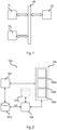
- Figure 2 shows a block diagram of an embodiment of a digital processing system 10a, such as a micro-controller.
- the processing system 10a comprises at least one processing unit 102, such as a microprocessor, usually the Central Processing Unit (CPU), programmed via software instructions.
- a processing unit 102 such as a microprocessor, usually the Central Processing Unit (CPU), programmed via software instructions.
- the software executed by the processing unit 102 is stored in a program memory 104a, such as a non-volatile memory, such as a Flash memory or EEPROM.
- the memory 104a may be integrated with the processing unit 102 in a single integrated circuit, or the memory 104a may be in the form of a separate integrated circuit and connected to the processing unit 102, e.g. via the traces of a printed circuit board.
- the memory 104a contains the firmware for the processing unit 102, wherein the term firmware includes both the software of a micro-processor and the programming data of a programmable logic circuits, such as a FPGA.
- the processing unit 102 may have associated one or more resources 106, such as:
- the digital processing systems 10a may support different functionalities.
- the processing systems may have different hardware architectures.
- the processing units 102 may have different architectures and processing speeds, and/or the number and type of the hardware resources 106 may vary.
- the behavior of the processing unit 102 is determined by the firmware stored in the memory 104a, e.g ., the software instructions to be executed by a microprocessor 102 of a micro-controller 10a.
- the firmware stored in the memory 104a
- the software instructions to be executed by a microprocessor 102 of a micro-controller 10a can be used for different applications.
- the behavior of the processing system 10a may also be varied based on configuration data written, e.g. during the production stage.
- these configuration data may be written into specific areas of the non-volatile memory 104a and retrieved when the processing system 10a is powered on.
- the configuration data may be stored in an additional non-volatile memory 104b, such as a one-time programmable (OTP) memory, e.g. implemented with fuses.
- OTP one-time programmable
- the program memory 104a may be used, in case the blocks shown in Figure 2 are integrated in a common integrated circuit.
- an additional memory 104b may be used, in case the program memory 104a is an external memory, and only the other blocks are integrated in a common integrated circuit.
- the configuration data CD are stored in a non-volatile memory (104a and/or 104b) of the integrated circuit comprising the block requiring configuration data, such as the processing unit 102 and/or one or more of the hardware resources 106.
- configuration data CD are often calibration data used to guarantee that the hardware behavior is uniform, thereby compensating possible production process tolerances.
- this applies often to the calibration of analog components of the processing system, such as a temperature sensor, analog-to-digital converter, voltage reference, etc.
- a voltage monitor threshold level of an analog comparator could be "trimmed" to the exact intended value by adjusting some levels with configuration/calibration data, which are written by the producer of the hardware of the processing systems, e.g. the micro-controller producer.
- the configuration data CD may also be used to customize the behavior of the hardware, e.g., the hardware resources 106, according to different application needs. For example, once the firmware of the processing system has been stored in the processing system 10a, some configuration data may be written in order to deactivate the debug interface, which e.g. could be used to download the firmware of the processing system.
- a first part of the configuration data CD may be written by the producer of the hardware of the processing system (e.g ., the producer of an integrated circuit), and/or a second part of the configuration data CD may be written by the developer of the firmware of the processing system 10a.
- the programmed configuration data CD may be read during a reset phase, which usually starts as soon as the processing system 10a is powered on.
- the processing system 10a may comprise for this purpose a configuration module 108 configured to read the configuration data CD from the non-volatile memory 104a and/or 104b, and distribute these configuration data CD within the processing system 10a.
- a configuration module 108 configured to read the configuration data CD from the non-volatile memory 104a and/or 104b, and distribute these configuration data CD within the processing system 10a.
- Figure 3 shows a possible embodiment for distributing the configuration data in the processing system 10a of Figure 2 .
- one or more configuration data CD are stored in one or more non-volatile memories 104 (i.e ., memories 104a and/or 104b). In various embodiments, these configuration data CD are stored in reserved memory areas, e.g. in the form of a plurality of consecutive memory locations.
- the configuration module 108 accesses the reserved memory areas containing the configuration data CD, reads the configuration data CD and transmits the configuration data CD to a respective block 110 within the processing system 10a.
- the block 110 may corresponds to any block of the processing system 10a requiring configuration data and may correspond to the processing unit 102, a hardware resource 106, or even a memory (e.g. the memory 104a).
- the block 110 may be a power management controller of the processing system 10a, which may be configured to receive some calibration data for the internal voltage level trimming, and/or the various IPs, such as the hardware resources 106, whose behavior can be tailored by the customer according to their needs.
- each block 110 may have associated a respective configuration data client 112.
- each configuration data client 112 may be associated univocally to a single hardware block 110, and provided configuration data only to the associated hardware block 110, e.g. a specific hardware resource 106, or may be associated with a plurality of hardware blocks 110, e.g. a plurality of hardware resource 106.
- the configuration data clients 112a, 112b and 112c may also be integrated in the respective block 110a, 110b and 110c.
- the configuration module 108 may determine the respective configuration data (selected from the configuration data CD) for each target block 110 to be configured and transmit the configuration data associated with the target block to the configuration data client 112 associated with the target block 110. Similarly, while reading the configuration data CD from the memory 104, the configuration module 108 may determine the target block(s) for the current configuration information and send the current configuration data to the configuration data client(s) associated with the respective target block(s). Generally, any communication may be used for transmitting the configuration data to the configuration data client 112, including both serial and parallel communications. For example, the configuration module 108 and the configuration data clients 112 may be connected via a bus 114, and each configuration data clients 112 may have associated a respective target address.
- each configuration data client 112 is configured to receive the configuration data from the module 108, store them into the internal register, e.g. store them into one or more internal flip-flops or latches.
- the data stored in the register may then be used to generate one or more signals which influence the behavior of one or more hardware blocks 110.
- the register may comprise a bit providing a flag specifying whether a certain protection (e.g. the possibility to write a certain area of the non-volatile memory) over some internal assets shall be applied or not, wherein this flag is provided to the hardware block in charge of enforcing this protection.
- the module 108 distributes the configuration data CD preferably during the reset phase.
- the processing system 10a may be kept in the reset phase.
- the reset phase is usually considered both a safe and secured state, e.g ., because when the processing system 10a (in particular the processing unit 102 and possibly the resources 106) is under reset, it usually cannot make damage to system it belongs to and it cannot be attacked as well.
- availability and testability of the processing system 10a may not be ensured.
- availability might be an issue, especially for the Car2X and autonomous driving world, where the system should be ready to react to its inputs, i.e ., the run-time functionalities provided by the processing system 10a should be available.
- testability is almost impossible when the processing system 10a is kept under reset, e.g., upon a failure, i.e . the processing system 10a is unable to make a diagnosis of possible malfunctions.
- the processing system 10a described with respect to Figures 2 and 3 is thus modified in order to permit, even in case of malfunction, safety, security, availability, and testability of the processing system 10a.
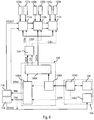
- FIG. 4 shows in this regard a second embodiment of a processing system 10a in accordance with the present invention.
- the processing system 10a comprises a configuration module 108 configured to read the configuration data CD form one or more non-volatile memories 104 (e.g ., memories 104a and/or 104b, and a plurality of configuration data clients 112 configured to receive respective configuration data from the module 108 and distribute them among a plurality of blocks 110 (not shown) requiring configuration data.
- each configuration data client 112 may be associate univocally with a respective block 110.
- the processing system 10a comprises again three configuration data clients 112a, 112b and 112c.
- the configuration module 108 comprises a data read module 1080 configured to read the configuration data CD from the memory 104 and a dispatch module 1082 configured to transmit the configuration data to the configuration data clients 112.
- any communication may be used for communication between the dispatch module 1082 and the configuration data clients 112.
- the communication between the dispatch module 1082 and the configuration data clients 112 is based on a data frames in accordance with a given format, called in the following Device Configuration Format (DCF).
- DCF Device Configuration Format
- each data frame comprises two fields: the payload (i.e ., the real data), called DCF Format payload, and possible additional data attributes used to identify the receiver of the data, called DCF Format attributes, wherein the receiver is one of the configuration data clients 112 representing a DCF client.
- the data attributes may consist in 16 or 32 bits, wherein a given number of bits specifies the address of one of the configuration data clients 112, and the payload may consist in 16 or 32 bits.
- the data read module 1080 is configured to read blocks of 64 bits from the memory 104, wherein the first 32 bits contain the data attributes (including the address of a configuration data client) and the second 32 bits contain the configuration data to be transmitted to the address specified in the data attributes.
- each configuration data client/DCF client 112 may be a hardware module, usually comprising a combinational circuit configured to store the received data in an internal register implemented, e.g ., with flip-flops/latches, thereby permitting to distribute, via one or more internal signals generated as a function of the data stored in the internal register, the configuration data received to various parts of the associate hardware block(s) 110.
- each configuration data client 112 may have associated a univocal address (i.e. , univocal within each processing system 10a) and analyse the data transmitted by the dispatch module 1082 in order to determine whether the additional data attributes (DCF Format attributes) contain the address associated with the configuration data client 112.
- the module 108 comprises an error and diagnostic module 1084 configured to manage the various modes of operation of the processing system 10a.
- corrupted data may be detected by storing one of more additional check bits together with the configuration data CD in the memory 104.
- these additional bits may be analyzed and compared with the configuration data read directly by a memory interface 1040 of the memory 104, or by the error and diagnostic module 1084.
- the memory interface 1040 of the memory 104 may be used, in case the memory contains additional check bits for all data stored in the non-volatile memory 104, i.e ., the memory may be a memory with ECC (Error-Correcting Code).
- ECC Error-Correcting Code
- the memory interface 1040 may generate an error signal ERR when the data read from the memory 104 are corrupted.
- the error and diagnostic module 1084 may analyze the configuration data CD and the additional check bits, in case the additional check bits are stored only for the configuration data CD, e.g. when the additional check bits are stored in the data attributes field.
- the error and diagnostic module 1084 may analyze the configuration data CD read from the memory 104 in order to determine invalid configuration data.
- each configuration data client 112 may also verify the configuration data received and determine whether the respective configuration data are valid. In this case, each configuration data client 112 may signal an error to the error and diagnostic module 1084 indicating that the received configuration data are invalid.
- the error and diagnostic module 1084 may generate a reset mode signal RM for the reset module 116 of the processing system 10a in order to activate the reset state.
- this step is purely optional, because the reset module 116 could also activate automatically the reset state.
- the specific implementation of the reset module 116 depends on architecture of the processing system. For example, the reset module 116 may generate a reset pulse of a given number of clock cycles provided to the blocks 110 of the processing system 10a.
- the data read module 1080 may read the configuration data CD from the memory 104 and the error and diagnostic module 1084 may determine (directly or indirectly via the memory interface 1040 of the memory 104) whether the configuration data CD are corrupted. In various embodiments, the error and diagnostic module 1084 may also determine whether the configuration data are valid.
- the error and diagnostic module 1084 may send a signal to the dispatch module 1082 and the dispatch module 1082 may distribute the configuration data CD.
- the configuration data CD may be verified and distributed sequentially, or the complete configuration data CD may be read and verified before these data are indeed transmitted to the various configuration data clients 112.
- the dispatch module 1082 will distribute the configuration data CD, thereby activating the processing system 10a, i.e ., the various blocks 110 will use the configuration data CD stored in the memory 104 (normal operation mode).
- the error and diagnostic module 1084 may perform different tasks.
- the error and diagnostic module 1084 may drive the reset module 112 of the processing system 10a via the signal RM, in order to perform a new reset of the processing system 10a.
- the processing system 10a is kept in a reset mode when the configuration data are permanently corrupted or invalid.
- the processing system 10a may however support also further operation modes, such as a safe secure mode and/or a diagnostic mode.
- the error and diagnostic module 1084 may activate the safe security mode by providing via the dispatch module 1082 a set of preset configuration data to the configuration data clients.
- the preset configuration data may also be stored directly within each configuration data client 112 and the error and diagnostic module 1084 may inform the configuration data clients 112, e.g., via a safe secure mode signal SSM, that the preset configuration data should be used.
- these preset configuration data correspond to configuration data for operating the various blocks 110 in an ISO 26262 "degraded" mode, wherein preferably additional security features are activated. Accordingly, once each configuration data client 112 has stored the preset configuration data in the internal register, the processing system 10a is started and the various blocks 110 will use the preset configuration data.
- the error and diagnostic module 1084 may activate the diagnostic mode by activating via a diagnostic mode signal DM a diagnostic module 118, so called design for testability (DFT), of the processing system 10a.
- DFT design for testability
- the diagnostic module 118 depends on the architecture of the processing system.
- the diagnostic block 118 may be configured to instruct the various blocks 110 of the processing system 10a to perform a given sequence of tasks, thereby executing a predefines test cycle. For example, during the test cycle, the blocks 110 may be instructed to generate given output signals at the pins of the processing system 10a.
- the error and diagnostic module 1084 may activate one of the following error states:
- the above modes of operation are not mutually exclusive, but as will be described in the following, different combinations of them are possible by providing appropriate preset configuration information to the various blocks 110, and activating or deactivating the reset module 116 and the diagnostic module 118.
- some blocks 110 may use the configuration data stored in the memory 104, while the blocks 110 with corrupted/invalid configuration data may use the preset configuration data.
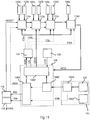
- FIG. 5 shows a possible embodiment of the above operations.
- the complete management of the operation modes of the processing system 10a is again managed by the error and diagnostic module 1084, representing thus a mode selection circuit.
- the configuration data CD are stored in the non-volatile memory 104, which is configure to determine whether the configuration data are corrupted.
- the memory 104 comprises a memory interface 1040 configured to determine, e.g., based on additional ECC bits stored in the memory 104, a signal ERR indicating whether the configuration data CD are corrupted.
- the data read module 1080 is configured to read the configuration data CD from the memory 104 and the memory 104 signals also whether the data read are corrupted, e.g. via the signal ERR transmitted to the module 1084.
- the dispatch module 1082 provides the configuration data read from the memory to the various configuration data clients 112.
- the dispatch module 1082 may generate a data signal DATA having a given number of bits (corresponding to the bits of the payload) containing the configuration data to be transmitted to a given configuration data client 112 and further control signals for selecting the target configuration data client (i.e. the additional data attributes).
- the dispatch module 1082 generates also an address signal ADR containing the address of the target configuration data client 112 and optionally a chip select signal CS used to signal to the configuration data clients 112 that the address signal ADD and the data signal DATA are valid.
- the address signal ADR (and the chip select signal CS) may be provided to a decoder 124 configured to activate one of the configuration data clients 112 as a function of the address signal ADD.
- the decoder 124 may set a chip select signal CSa in order to indicate that the configuration data client 112a should read the data signal DATA when the address signal ADD corresponds to an address assigned to the configuration data client 112a (and the chip select signal CS is set).
- the decoder 124 may set a chip select signal CSb in order to indicate that the configuration data client 112b should read the data signal DATA when the address signal ADR corresponds to an address assigned to the configuration data client 112b (and the chip select signal CS is set), etc.
- each configuration data client 112 may receive at input various data signals, selected as a function of a reset signal RESET generate by the reset module 112 and the safe security mode SSM signal generated by the module 108, in particular the error and diagnostic module 1084:
- Figure 7 shows a possible embodiment of the configuration data client 112a which may be used in the embodiment shown in Figure 6 .
- the same architecture may also be used for the other configuration data client.
- the configuration data client 120a has associated reset data 120a and preset configuration data 122.
- these data are hardwired within the configuration data client 120a.
- the configuration data client 120a receives at input the configuration data DATA from the dispatch module.
- the configuration data client 120a is configured to store one of these data (reset, preset configuration data or received configuration data) in an internal register 1120 as a function of the chip select signal CSa, the safe secure mode signal SSM and the reset signal RESET.
- the configuration data client 120a comprises:
- the reset data 120a when the reset signal RESET is set, the reset data 120a will be stored in the register 1120. Conversely, when the reset signal is not set and the safe secure mode signal SSM is set, the preset configuration data 122a will be stored in the register 1120. Conversely, if both signal are not set, the chip select signal CSa determines whether the data DATA or the previous configuration data CDa should be stored in the register 1120.
- the switching between the various operation states of the processing system 10a is managed by the error and diagnostic module 1084.
- the module 1084 may support the following modes:
- the module 1084 activates the reset mode when the processing system 10a is switched on. During this mode, the module 1084 drives the reset module 116, which thus generates the reset signal RESET and the various configuration data clients load the reset data into the internal register.
- the module 108 reads via the data read module 1080 the configuration data CD from the non-volatile memory 104 and transmits the configuration data read to the various configuration data clients 112, thereby overwriting the reset data.
- the error and diagnostic module 1084 may enable the safe secure mode and/or the diagnostic mode.
- the error and diagnostic module 1084 may activate the safe secure mode by setting the signal SSM, whereby the configuration data clients 112 read the respective preset configuration data 122.
- the error and diagnostic module 1084 may activate the diagnostic mode by sending a signal DM to the diagnostic module 118.
- This diagnostic module 114 may then activate diagnostic functions in the various blocks 110.
- the memory 104 may comprise a test logic 1042 configured to verify the non-volatile memory 104 and a signal DIAG generated by the diagnostic module 118 or directly the signal DM may be used to activate this test logic 1042.
- the error and diagnostic module 1084 requires some additional information in order to decide whether the safe secure mode and/or the diagnostic mode should be activated.
- this information representing mode configuration data MCD, may be stored in a non-volatile memory, such as a one-time programmable memory, associated with the module 108. Conversely, in other embodiments, this information is stored in the non-volatile memory 104.
- the mode configuration data are encoded with plurality of bits, wherein:
- a single keyword/bit sequence may be used for all blocks 110, i.e. the error and diagnostic module 1084 is configured to activate the safe secure mode and/or the diagnostic mode for all blocks 110.
- a respective keyword/bit sequence may be stored for each block 110, i.e. the error and diagnostic module 1084 is configured to selectively activate the safe secure mode and/or the diagnostic mode for each block 110.
- the memory 104 may provide the mode configuration data MCD consisting in a given number of bits, such as 32 bits, wherein a first subset of the bits, e.g ., the bits [31:16], are associated with the diagnostic mode, and a second subset of the bits, e.g., the bits [15:0], are associated with the safe secure mode.
- the module 1084 may activate the diagnostic mode by setting the signal DIAG, and when the second subset of bits corresponds to a given reference bit sequence, e.g ., 0x5E5A, the module 1084 may activate the safe secure mode by setting the signal SSM.
- the module 1084 may activate the reset mode via the reset module 116. Accordingly, in the embodiment considered, the reset mode is also activated when bits of the mode configuration data MCD are corrupted.
- the use of a plurality of bits for the first and second subset of bits ensures that a single bit error of these mode configuration data MCD may not activate incidentally the diagnostic mode or the safe secure mode, but at most the reset state is activated.
- the mode configuration data MCD may be stored directly in the non-volatile memory 104, i.e ., the memory in which are also stored the configuration data CD.
- the mode configuration data are stored at one or more fixed memory locations of the non-volatile memory or together with the configuration data.
- Figure 9 shows an embodiment, in which the mode configuration data MCD are stored at one or more fixed memory locations.
- the module 108 may read the mode configuration data MCD via the data read module 1080 and store them in an internal register 1086.
- the module 1084 may compare the mode configuration data MCD stored in the internal register 1086 with the respective reference bit sequences in order to decide which error more (reset, diagnostic or safe secure mode) should be activated.
- the module 108 may extract the mode configuration data and store them in the internal register 1086.
- Figure 10 shows an embodiment, in which an additional configuration data client 112d is used.
- the configuration data client 112d is configured to store in an internal register during a reset state a given reset value 120d and overwrite the reset values by storing the data received from the module 108.
- the configuration data client 112d may have associated a respective address ADR.
- the decoder 124 may generate a chip select signal CSd when the address ADR provided by the module 108 corresponds to the address associated with the configuration data client 112d.
- the configuration data client 112d does not have associated preset values 122d. For this reason, the multiplexer 1124 in Figure 7 may also be omitted.
- the architecture of the other configuration data clients 112 may be used, by simply setting the respective preset configuration data 122 to the reset values 120.
- the configuration module 108 in particular the dispatch module 1082, distributes the configuration data CD read from the memory 104 to the various configuration data clients 112, without knowing that these data include also the mode configuration data MCD.
- the configuration data client 112d represents thus the configuration data client associated with the configuration module 108, wherein the configuration data client 112d provides the mode configuration data MCD the configuration module 108, in particular the error and diagnostic module 1084.
- the module 108 passes the mode configuration data read from the memory 104 to the configuration data client 112d and receives from the same the stored configuration data, i.e., the mode configuration data MCD.
- the memory interface 1042 may report via the signal ERR a data error to the module 108 and the error and diagnostic module 1084 may determine the reaction of the processing systems 10a by means of the signals SSM, DM and RM.
- the module 1082 may trigger a new reset by driving the reset module 112 via the signal RM. Accordingly, the processing system 10a (including the blocks 110 and the also the configuration module 108) will perform a new restart. The configuration data clients 112 will thus re-load the default reset values 120 (which is fixed at design time) in response to the reset signal RESET generate by the reset module 116. Next, the configuration module 108 will perform a new attempt to read the configuration data CD from the non-volatile memory 104. Accordingly, in case the configuration data are permanently corrupted, the processing system 10a may be kept in the reset mode by performing an infinite number of reset loops. Generally, the configuration module 108 may also monitor the number of resets performed and interrupt the reset loop.
- the mode configuration data MCD may indicate that the preset configuration data 122 should be used.
- this mode may only be activated once the configuration module 108 has read the mode configuration data MCD from the memory 104 (and possibly transmitted to the configuration data client 112d).
- the error and diagnostic module 1084 Once activated, the error and diagnostic module 1084 generates the signal SSM, and the configuration data clients 112 associated with the blocks 110 (in particular the clients 112a-112c) will load the preset configuration data 122.
- the configuration data client 112d associated with the module 108 may not have associates preset configuration data 122.
- the preset configuration data 122 may be fixed during the design of the processing system 10a, e.g., hardwired. As mentioned before, each block 110 should be designed that in response to the preset configuration data 122, the block 110 should still be able to operate, possibly with reduced device functionality. Accordingly, once the signal SSM is set, the configuration data clients 112a-112c will replace the reset data 120 (or already loaded configuration data) with the preset configuration data 122.
- the error and diagnostic module 1084 may generate the signal DM in order to activate the diagnostic module 118, which e.g. performs one or more system tests.
- this mode may only be activated once the configuration module 108 has read the mode configuration data MCD from the memory 104 (and possibly transmitted to the configuration data client 112d). For example, once activated, several internal signals might be exposed on some internal non-bonded pads. Another possibility is that the non-volatile memory 104 might enable some test features on some areas of the memory that usually cannot be analyzed for security reason.
- configuration data may relate to security aspects, such as a cipher key to be used by a hardware secure element.
- security related configuration data are usually stored in separate memory locations or a separate non-volatile memory.
- these security related configuration data are stored in encrypted format and the memory interface may be configured to decrypt these data.
- each block 110 may have associated two or more independent configuration data clients 112, e.g., one for the non-security related configuration data and another for the security related configuration data.
- the above modes may thus be activated by writing the mode configuration data into the memory 104.
- at least the diagnostic mode may provide sensible data from a security point of reason, e.g. because the memory interface 1040 could perform a sequential readout of the data stored in the memory 104 and make the data available via one or more pads of the processing system 10a.
- Figure 11 shows in this regard an embodiment, in which the configuration module 108 is configured to take into account also the life cycle of the processing system.
- this life cycle may be encoded with a bit sequence.
- this bit sequence is stored in a non-volatile memory 126, preferably a one-time programmable memory.
- this life cycle data LCD may also be stored at reserved memory locations of the memory 104.
- bit sequence LCD stored in the memory 122 may indicate one of the following stages:
- the error and diagnostic module 1084 may not only take into account the mode configuration data MCD but also the product life cycle as indicated by the bit sequence LCD stored in the memory 126.
- the configuration module 108 may distribute the configuration data CD to the configuration data clients 112 and the processing system 10a is normally operated with these configuration data, i.e. the mode configuration data MCD and the product life cycle data LCD are not taken into account at all.
- the configuration module 108 uses these data only when the configuration data CD are corrupted (or invalid).
- the configuration module 108 may use the mode configuration data MCD, which may indicate that any of the previous modes may be activated (i.e., reset, diagnostic, safe secure or both diagnostic and safe secure).
- the reset mode corresponds to the default mode, which is used, e.g ., in case the mode configuration data are corrupted (or invalid)
- the configuration module 108 may disregard the mode configuration data MCD and the reset mode may be used by default.
- the module 108 may only permit an activation of the safe secure mode as an alternative to the default reset mode, i.e. the configuration module 108 may activate the safe secure mode only when the mode configuration data MCD indicate that the safe secure mode should be used.
- the diagnostic mode can only be activated by the producer of the processing system 10a, but cannot be activated, e.g., when the processing system 10a is indeed used ("in field" stage).
- this mode corresponds in general to a downgraded mode, in which preset configuration data are used.
- the preset configuration data may activate also these security related features.
Landscapes
- Engineering & Computer Science (AREA)
- Theoretical Computer Science (AREA)
- General Engineering & Computer Science (AREA)
- Quality & Reliability (AREA)
- Physics & Mathematics (AREA)
- General Physics & Mathematics (AREA)
- Health & Medical Sciences (AREA)
- Biomedical Technology (AREA)
- Computer Hardware Design (AREA)
- Techniques For Improving Reliability Of Storages (AREA)
- Automation & Control Theory (AREA)
- Human Computer Interaction (AREA)
- Transportation (AREA)
- Mechanical Engineering (AREA)
Abstract
- receive mode configuration data (MDU);
- read the configuration data (CD) from the non-volatile memory (104);
- test whether the configuration data (CD) contain errors by verifying whether the configuration data (CD) are corrupted and/or invalid;
- in case the configuration data (CD) do not contain errors, activating a normal operation mode of the processing system (10a) by providing the configuration data (CD) read from the non-volatile memory (104) to the at least one hardware block (110); and
- in case the configuration data (CD) do contain errors, activating an error operation mode of the processing system (10a) as a function of the mode configuration data (MDU) by:
- providing reset values (120) to the at least one hardware block (110) when the mode configuration data (MDU) indicate that a reset mode should be activated; and
- providing preset configuration data (122) to the at least one hardware block (110) when the mode configuration data (MDU) indicate that a degraded mode should be activated.
Description
- Embodiments of the present disclosure relate to processing systems, such as micro-controllers, having associated a memory in which configuration data are stored.
-
Figure 1 shows a typical electronic system, such as the electronic system of a vehicle, comprising a plurality ofprocessing systems 10, such as embedded systems or integrated circuits, e.g., a FPGA (Field Programmable Gate Array), DSP (Digital Signal Processor) or a micro-controller (e.g., dedicated to the automotive market). - For example, in
Figure 1 are shown threeprocessing systems suitable communication system 20. For example, the communication system may include a vehicle control bus, such as a CAN (Controller Area Network) bus, and possibly a multimedia bus, such as a MOST (Media Oriented Systems Transport) bus, connected to vehicle control bus via a gateway. Typically, theprocessing systems 10 are located at different positions of the vehicle and may include, e.g., an Engine Control Unit (ECU), a Transmission Control Unit (TCU), an Anti-lock Braking System (ABS), a body control modules (BCM), and/or a navigation and/or multimedia audio system. - Future generation of processing systems, in particular micro-controllers dedicated to automotive applications, will exhibit a significant increase in complexity, mainly due to the increasing number of functionalities (such as new protocols, new features, etc.) and to the tight constraints concerning the operation conditions of the system (such as lower power consumption, increased calculation power and speed, etc.). For example, complexity is expected to increase in particular in the context of the forthcoming Car2X and autonomous driving world, because safety and security of the
processing systems 10 will become more and more relevant. - Usually, safety is intended to guarantee the functionality in case of both random and systematic faults, e.g., due to the corruption of "functional-critical" configuration data programmed during the production of the micro-controller, such as calibration data or other types of configuration data used to trim and/or configure the device functionalities. For example, the specification ISO 26262 dictates a complete process and the requirements to achieve a functionality being compliant within the chosen safety goals.
- Conversely, security is intended to guarantee the protection of the internal resources against malicious attacks, which, for example, might lead to the corruption of the above mentioned data. For example, encryption of the communications between the various systems will become mandatory for the upcoming Car2X and autonomous driving scenario.
- Thus, while achieving different and possible diverging goals, safety and security should be treated in conjunction. For example, this becomes evident when considering a possible abnormal behavior of a
processing system 10 of the vehicle. From a safety point of view, the micro-controller should still be able to operate permitting an operation of the vehicle, even in a "degraded" mode. Conversely, from security point of view, it might be advisable to stop the car, e.g., because the car might have been hacked. Unfortunately, the distinction of malfunctions or security faults may often not be taken, e.g., because often it is rather difficult to determine the actual failure root. - In view of the above, it is an objective of various embodiments of the present disclosure to provide solutions able to improve safety, security and diagnosis tasks of a processing system, such as a micro-controller.
- According to one or more embodiments, one or more of the above objectives is achieved by means of a processing system having the features specifically set forth in the claims that follow. Embodiments moreover concern a related integrated circuit, device and method.
- The claims are an integral part of the technical teaching of the disclosure provided herein.
- As mentioned before, various embodiments of the present disclosure provide solutions for managing the operation of a processing system.
- In various embodiments, the processing system comprises at least one hardware block configured to change operation as a function of configuration data, a non-volatile memory comprising the configuration data for the at least one hardware block, and configuration means configured to read the configuration data from the non-volatile memory and provide the configuration data read from the non-volatile memory to the at least one hardware block. For example, in various embodiments, the processing system may comprise a processing unit, such as a microprocessor, and the configuration data may be stored in the non-volatile program memory for storing the firmware of the processing unit.
- Specifically, in various embodiments, the configuration means are configured to receive mode configuration data, read the configuration data from the non-volatile memory and test whether the configuration data contain errors by verifying whether the configuration data are corrupted and/or invalid.
- In various embodiments, in case the configuration data do not contain errors, the configuration means may activate a normal operation mode of the processing system by providing the configuration data read from the non-volatile memory to the at least one hardware block.
- Conversely, in various embodiments, in case the configuration data do contain errors, the configuration means may activate an error operation mode of the processing system as a function of the mode configuration data. For example, the configuration means may provide reset values to the at least one hardware block when the mode configuration data indicate that a reset mode should be activated, and provide preset configuration data to the at least one hardware block when the mode configuration data indicate that a degraded mode should be activated. In various embodiments, the configuration means, may also activate a diagnostic module of the processing system when the mode configuration data indicate that a diagnostic mode should be activated.
- For example, in various embodiments, the configuration means comprise at least one configuration data client comprising a register for storing configuration data, wherein the configuration data stored in the register are provided to at least one hardware block.
- In this case, the configuration means may also comprise a configuration module. For example, the configuration module may comprise a hardware data read module configured to read the configuration data from the non-volatile memory and a hardware dispatch module configured to send the configuration data read from the non-volatile memory to the at least one configuration data client. For example, each configuration data client may have associated a respective address, and the hardware dispatch module may send the configuration data to the configuration data clients in the form of data packets addressed to a given configuration data client.
- In various embodiments, the configuration module comprises also a hardware error and diagnostic module configured to test whether the configuration data contain errors by verifying whether the configuration data are corrupted and/or invalid, and in case the configuration data do contain errors, the error and diagnostic module may activate an error operation mode of the processing system as a function of the mode configuration data. Specifically, the error and diagnostic module may:
- set a degraded mode signal when the mode configuration data indicate that the degraded mode should be activated;
- optionally set a diagnostic mode signal provided to the diagnostic module of the processing system when the mode configuration data indicate that the diagnostic mode should be activated; and
- set a reset mode signal provided to a reset module of the processing system when the mode configuration data indicate that the reset mode should be activated.
- In this case, one or more of the configuration data clients may be configured to:
- when the reset module indicates that a reset should be performed, store the reset values in the register;
- when the degraded mode signal is set, store the preset configuration data in the register, and
- otherwise, store the configuration data received from the hardware dispatch module in the register.
- In various embodiments, the mode configuration data are stored in the non-volatile memory comprising also the configuration data. In this case, also the configuration module may have associated a configuration data client, i.e., the configuration module may read via the data read module the mode configuration data from the non-volatile memory and send the mode configuration data via the dispatch module to the configuration data client associated with the configuration module. Accordingly, the error and diagnostic module may receive the mode configuration data from the configuration data client associated with the configuration module.
- In various embodiments, the configuration means may also activate the error operation mode of the processing system as a function of additional life cycle data.
- Embodiments of the present disclosure will now be described with reference to the annexed drawings, which are provided purely by way of non-limiting example and in which:
-
Figure 1 shows a typical electronic system; -
Figure 2 shows an embodiment of a processing systems comprising a configuration module in accordance with the present disclosure; -
Figure 3 shows the general architecture of an embodiment of a processing system comprising a configuration module and configuration data clients in accordance with the present disclosure; -
Figure 4 shows a first embodiment of a processing system comprising a configuration module and configuration data clients in accordance with the present disclosure; -
Figure 5 shows a second embodiment of a processing system comprising a configuration module and configuration data clients in accordance with the present disclosure; -
Figure 6 shows a third embodiment of a processing system comprising a configuration module and configuration data clients in accordance with the present disclosure; -
Figure 7 shows an embodiment of a configuration data client adapted to be used in the processing systems ofFigure 6 ; -
Figure 8 shows an embodiment of mode configuration data adapted to be used to set the behavior of the configuration module; -
Figure 9 shows a first embodiment of a processing system comprising a configuration module and configuration data clients in accordance with the present disclosure, wherein mode configuration data are used to set the behavior of the configuration module; -
Figure 10 shows a second embodiment of a processing system comprising a configuration module and configuration data clients in accordance with the present disclosure, wherein mode configuration data are used to set the behavior of the configuration module; and -
Figure 11 shows an embodiment of a processing system comprising a configuration module and configuration data clients in accordance with the present disclosure, wherein life cycle data are used to set the behavior of the configuration module. - In the following description, numerous specific details are given to provide a thorough understanding of embodiments. The embodiments can be practiced without one or several specific details, or with other methods, components, materials, etc. In other instances, well-known structures, materials, or operations are not shown or described in detail to avoid obscuring aspects of the embodiments.
- Reference throughout this specification to "one embodiment" or "an embodiment" means that a particular feature, structure, or characteristic described in connection with the embodiment is included in at least one embodiment. Thus, the appearances of the phrases "in one embodiment" or "in an embodiment" in various places throughout this specification are not necessarily all referring to the same embodiment. Furthermore, the particular features, structures, or characteristics may be combined in any suitable manner in one or more embodiments.
- The headings provided herein are for convenience only and do not interpret the scope or meaning of the embodiments.
- In the following
Figures 2 to 11 parts, elements or components which have already been described with reference toFigure 1 are denoted by the same references previously used in such Figures; the description of such previously described elements will not be repeated in the following in order not to overburden the present detailed description. -
Figure 2 shows a block diagram of an embodiment of adigital processing system 10a, such as a micro-controller. - In the embodiment considered, the
processing system 10a comprises at least oneprocessing unit 102, such as a microprocessor, usually the Central Processing Unit (CPU), programmed via software instructions. Usually, the software executed by theprocessing unit 102 is stored in aprogram memory 104a, such as a non-volatile memory, such as a Flash memory or EEPROM. Generally, thememory 104a may be integrated with theprocessing unit 102 in a single integrated circuit, or thememory 104a may be in the form of a separate integrated circuit and connected to theprocessing unit 102, e.g. via the traces of a printed circuit board. Thus, in general thememory 104a contains the firmware for theprocessing unit 102, wherein the term firmware includes both the software of a micro-processor and the programming data of a programmable logic circuits, such as a FPGA. - In the embodiment considered, the
processing unit 102 may have associated one ormore resources 106, such as: - one or more communication interfaces, such as UART (Universal asynchronous receiver/transmitter), SPI (Serial Peripheral Interface Bus), I2C (Inter-Integrated Circuit), CAN bus (Controller Area Network), Ethernet, a debug interface; and/or
- one or more analog-to-digital and/or digital-to-analog converters; and/or
- one or more dedicated digital components, such as hardware timers and/or counters, or a cryptographic co-processor; and/or
- one or more analog components, such as comparators, sensors, such as a temperature sensor, etc.; and/or
- one or more mixed signal components, such as a PWM (Pulse-Width Modulation) driver.
- Accordingly, the
digital processing systems 10a may support different functionalities. - For example, the processing systems may have different hardware architectures. For example, the
processing units 102 may have different architectures and processing speeds, and/or the number and type of thehardware resources 106 may vary. - Moreover, even assuming a substantially identical hardware architecture, the behavior of the
processing unit 102 is determined by the firmware stored in thememory 104a, e.g., the software instructions to be executed by amicroprocessor 102 of amicro-controller 10a. Thus, by installing a different firmware, the same hardware (micro-controller) can be used for different applications. - Often, the behavior of the
processing system 10a may also be varied based on configuration data written, e.g. during the production stage. For example, these configuration data may be written into specific areas of thenon-volatile memory 104a and retrieved when theprocessing system 10a is powered on. Alternatively or in addition, the configuration data may be stored in an additionalnon-volatile memory 104b, such as a one-time programmable (OTP) memory, e.g. implemented with fuses. - For example, the
program memory 104a may be used, in case the blocks shown inFigure 2 are integrated in a common integrated circuit. Conversely, anadditional memory 104b may be used, in case theprogram memory 104a is an external memory, and only the other blocks are integrated in a common integrated circuit. Accordingly, in various embodiments, the configuration data CD are stored in a non-volatile memory (104a and/or 104b) of the integrated circuit comprising the block requiring configuration data, such as theprocessing unit 102 and/or one or more of thehardware resources 106. - For example, such configuration data CD are often calibration data used to guarantee that the hardware behavior is uniform, thereby compensating possible production process tolerances. For example, this applies often to the calibration of analog components of the processing system, such as a temperature sensor, analog-to-digital converter, voltage reference, etc. For example, a voltage monitor threshold level of an analog comparator could be "trimmed" to the exact intended value by adjusting some levels with configuration/calibration data, which are written by the producer of the hardware of the processing systems, e.g. the micro-controller producer.
- However, the configuration data CD may also be used to customize the behavior of the hardware, e.g., the
hardware resources 106, according to different application needs. For example, once the firmware of the processing system has been stored in theprocessing system 10a, some configuration data may be written in order to deactivate the debug interface, which e.g. could be used to download the firmware of the processing system. - Thus, generally a first part of the configuration data CD may be written by the producer of the hardware of the processing system (e.g., the producer of an integrated circuit), and/or a second part of the configuration data CD may be written by the developer of the firmware of the
processing system 10a. - As mentioned before, the programmed configuration data CD may be read during a reset phase, which usually starts as soon as the
processing system 10a is powered on. - Specifically, as shown in
Figure 2 , theprocessing system 10a may comprise for this purpose aconfiguration module 108 configured to read the configuration data CD from thenon-volatile memory 104a and/or 104b, and distribute these configuration data CD within theprocessing system 10a. - For example,
Figure 3 shows a possible embodiment for distributing the configuration data in theprocessing system 10a ofFigure 2 . - In the embodiment considered, one or more configuration data CD are stored in one or more non-volatile memories 104 (i.e.,
memories 104a and/or 104b). In various embodiments, these configuration data CD are stored in reserved memory areas, e.g. in the form of a plurality of consecutive memory locations. - Accordingly, in the embodiment considered, the
configuration module 108 accesses the reserved memory areas containing the configuration data CD, reads the configuration data CD and transmits the configuration data CD to a respective block 110 within theprocessing system 10a. Generally, the block 110 may corresponds to any block of theprocessing system 10a requiring configuration data and may correspond to theprocessing unit 102, ahardware resource 106, or even a memory (e.g. thememory 104a). For example, the block 110 may be a power management controller of theprocessing system 10a, which may be configured to receive some calibration data for the internal voltage level trimming, and/or the various IPs, such as thehardware resources 106, whose behavior can be tailored by the customer according to their needs. - In order to distribute the configuration data, each block 110 may have associated a respective configuration data client 112. For example, in
Figure 3 are shown threeblocks configuration data clients specific hardware resource 106, or may be associated with a plurality of hardware blocks 110, e.g. a plurality ofhardware resource 106. In general, theconfiguration data clients respective block - Accordingly, in the embodiment considered, the
configuration module 108 may determine the respective configuration data (selected from the configuration data CD) for each target block 110 to be configured and transmit the configuration data associated with the target block to the configuration data client 112 associated with the target block 110. Similarly, while reading the configuration data CD from thememory 104, theconfiguration module 108 may determine the target block(s) for the current configuration information and send the current configuration data to the configuration data client(s) associated with the respective target block(s). Generally, any communication may be used for transmitting the configuration data to the configuration data client 112, including both serial and parallel communications. For example, theconfiguration module 108 and the configuration data clients 112 may be connected via abus 114, and each configuration data clients 112 may have associated a respective target address. - Accordingly, each configuration data client 112 is configured to receive the configuration data from the
module 108, store them into the internal register, e.g. store them into one or more internal flip-flops or latches. The data stored in the register may then be used to generate one or more signals which influence the behavior of one or more hardware blocks 110. For example, the register may comprise a bit providing a flag specifying whether a certain protection (e.g. the possibility to write a certain area of the non-volatile memory) over some internal assets shall be applied or not, wherein this flag is provided to the hardware block in charge of enforcing this protection. - Thus, as mentioned before, the
module 108 distributes the configuration data CD preferably during the reset phase. - However, the configuration data CD may also be corrupted. Accordingly, in this case, the
processing system 10a may be kept in the reset phase. In fact, the reset phase is usually considered both a safe and secured state, e.g., because when theprocessing system 10a (in particular theprocessing unit 102 and possibly the resources 106) is under reset, it usually cannot make damage to system it belongs to and it cannot be attacked as well. However, in the reset condition, availability and testability of theprocessing system 10a may not be ensured. However, availability might be an issue, especially for the Car2X and autonomous driving world, where the system should be ready to react to its inputs, i.e., the run-time functionalities provided by theprocessing system 10a should be available. Similarly, testability is almost impossible when theprocessing system 10a is kept under reset, e.g., upon a failure, i.e. theprocessing system 10a is unable to make a diagnosis of possible malfunctions. - In various embodiments, the
processing system 10a described with respect toFigures 2 and3 is thus modified in order to permit, even in case of malfunction, safety, security, availability, and testability of theprocessing system 10a. -
Figure 4 shows in this regard a second embodiment of aprocessing system 10a in accordance with the present invention. - Specifically, also in this case, the
processing system 10a comprises aconfiguration module 108 configured to read the configuration data CD form one or more non-volatile memories 104 (e.g.,memories 104a and/or 104b, and a plurality of configuration data clients 112 configured to receive respective configuration data from themodule 108 and distribute them among a plurality of blocks 110 (not shown) requiring configuration data. For example, as mentioned before, each configuration data client 112 may be associate univocally with a respective block 110. - For example, in the embodiment considered, the
processing system 10a comprises again threeconfiguration data clients - In the embodiment considered, the
configuration module 108 comprises adata read module 1080 configured to read the configuration data CD from thememory 104 and adispatch module 1082 configured to transmit the configuration data to the configuration data clients 112. - As mentioned before, any communication may be used for communication between the
dispatch module 1082 and the configuration data clients 112. For example, in various embodiments, the communication between thedispatch module 1082 and the configuration data clients 112 is based on a data frames in accordance with a given format, called in the following Device Configuration Format (DCF). For example, in various embodiments, each data frame comprises two fields: the payload (i.e., the real data), called DCF Format payload, and possible additional data attributes used to identify the receiver of the data, called DCF Format attributes, wherein the receiver is one of the configuration data clients 112 representing a DCF client. For example, the data attributes may consist in 16 or 32 bits, wherein a given number of bits specifies the address of one of the configuration data clients 112, and the payload may consist in 16 or 32 bits. For example, in various embodiments, the data readmodule 1080 is configured to read blocks of 64 bits from thememory 104, wherein the first 32 bits contain the data attributes (including the address of a configuration data client) and the second 32 bits contain the configuration data to be transmitted to the address specified in the data attributes. - As described before, each configuration data client/DCF client 112 may be a hardware module, usually comprising a combinational circuit configured to store the received data in an internal register implemented, e.g., with flip-flops/latches, thereby permitting to distribute, via one or more internal signals generated as a function of the data stored in the internal register, the configuration data received to various parts of the associate hardware block(s) 110. For example, as mentioned before, each configuration data client 112 may have associated a univocal address (i.e., univocal within each
processing system 10a) and analyse the data transmitted by thedispatch module 1082 in order to determine whether the additional data attributes (DCF Format attributes) contain the address associated with the configuration data client 112. - As mentioned before, the data read by the
module 108 from thenon-volatile memory 104 may also be corrupted or not valid, and themodule 108 should be able to activate different modes. Specifically, in the embodiment considered, themodule 108 comprises an error anddiagnostic module 1084 configured to manage the various modes of operation of theprocessing system 10a. - For example, in various embodiments, corrupted data may be detected by storing one of more additional check bits together with the configuration data CD in the
memory 104. Generally, these additional bits may be analyzed and compared with the configuration data read directly by amemory interface 1040 of thememory 104, or by the error anddiagnostic module 1084. For example, thememory interface 1040 of thememory 104 may be used, in case the memory contains additional check bits for all data stored in thenon-volatile memory 104, i.e., the memory may be a memory with ECC (Error-Correcting Code). For example, in this case thememory interface 1040 may generate an error signal ERR when the data read from thememory 104 are corrupted. Conversely, the error anddiagnostic module 1084 may analyze the configuration data CD and the additional check bits, in case the additional check bits are stored only for the configuration data CD, e.g. when the additional check bits are stored in the data attributes field. - Similarly, in various embodiments, the error and
diagnostic module 1084 may analyze the configuration data CD read from thememory 104 in order to determine invalid configuration data. Alternatively or in addition, each configuration data client 112 may also verify the configuration data received and determine whether the respective configuration data are valid. In this case, each configuration data client 112 may signal an error to the error anddiagnostic module 1084 indicating that the received configuration data are invalid. - Accordingly, in various embodiments, once the
processing system 10a is switched on, the error anddiagnostic module 1084 may generate a reset mode signal RM for thereset module 116 of theprocessing system 10a in order to activate the reset state. Generally, this step is purely optional, because thereset module 116 could also activate automatically the reset state. Those of skill in the art will appreciate that the specific implementation of thereset module 116 depends on architecture of the processing system. For example, thereset module 116 may generate a reset pulse of a given number of clock cycles provided to the blocks 110 of theprocessing system 10a. - Next, the data read
module 1080 may read the configuration data CD from thememory 104 and the error anddiagnostic module 1084 may determine (directly or indirectly via thememory interface 1040 of the memory 104) whether the configuration data CD are corrupted. In various embodiments, the error anddiagnostic module 1084 may also determine whether the configuration data are valid. - Thus, in case the error and
diagnostic module 1084 determines that the configuration data CD are not corrupted (and valid), the error anddiagnostic module 1084 may send a signal to thedispatch module 1082 and thedispatch module 1082 may distribute the configuration data CD. Generally, the configuration data CD may be verified and distributed sequentially, or the complete configuration data CD may be read and verified before these data are indeed transmitted to the various configuration data clients 112. - Thus, in the absence of error in the configuration data CD, the
dispatch module 1082 will distribute the configuration data CD, thereby activating theprocessing system 10a, i.e., the various blocks 110 will use the configuration data CD stored in the memory 104 (normal operation mode). - Conversely, when the error and
diagnostic module 1084 detects that the configuration data CD are corrupted (or invalid), the error anddiagnostic module 1084 may perform different tasks. - For example, in various embodiments, the error and
diagnostic module 1084 may drive the reset module 112 of theprocessing system 10a via the signal RM, in order to perform a new reset of theprocessing system 10a. Thus, in this case, theprocessing system 10a is kept in a reset mode when the configuration data are permanently corrupted or invalid. - In various embodiments, the
processing system 10a may however support also further operation modes, such as a safe secure mode and/or a diagnostic mode. - For example, in various embodiments, the error and
diagnostic module 1084 may activate the safe security mode by providing via the dispatch module 1082 a set of preset configuration data to the configuration data clients. Generally, the preset configuration data may also be stored directly within each configuration data client 112 and the error anddiagnostic module 1084 may inform the configuration data clients 112, e.g., via a safe secure mode signal SSM, that the preset configuration data should be used. In various embodiments, these preset configuration data correspond to configuration data for operating the various blocks 110 in an ISO 26262 "degraded" mode, wherein preferably additional security features are activated. Accordingly, once each configuration data client 112 has stored the preset configuration data in the internal register, theprocessing system 10a is started and the various blocks 110 will use the preset configuration data. - Conversely, the error and
diagnostic module 1084 may activate the diagnostic mode by activating via a diagnostic mode signal DM adiagnostic module 118, so called design for testability (DFT), of theprocessing system 10a. Those of skill in the art will appreciate that the specific implementation of thediagnostic module 118 depends on the architecture of the processing system. For example, thediagnostic block 118 may be configured to instruct the various blocks 110 of theprocessing system 10a to perform a given sequence of tasks, thereby executing a predefines test cycle. For example, during the test cycle, the blocks 110 may be instructed to generate given output signals at the pins of theprocessing system 10a. - Accordingly, in various embodiments, once having determined whether the configuration data CD are corrupted and/or valid, the error and
diagnostic module 1084 may activate one of the following error states: - normal operation mode, wherein the configuration data stored in the
memory 104 are used, - reset mode,
- safe secure mode, wherein the preset configuration data are used, or
- diagnostic mode.
- In various embodiments, the above modes of operation are not mutually exclusive, but as will be described in the following, different combinations of them are possible by providing appropriate preset configuration information to the various blocks 110, and activating or deactivating the
reset module 116 and thediagnostic module 118. Moreover, some blocks 110 may use the configuration data stored in thememory 104, while the blocks 110 with corrupted/invalid configuration data may use the preset configuration data. -
Figure 5 shows a possible embodiment of the above operations. - In the embodiment considered, the complete management of the operation modes of the
processing system 10a is again managed by the error anddiagnostic module 1084, representing thus a mode selection circuit. - Moreover, in the embodiment considered, the configuration data CD are stored in the
non-volatile memory 104, which is configure to determine whether the configuration data are corrupted. For example, in the embodiment considered, thememory 104 comprises amemory interface 1040 configured to determine, e.g., based on additional ECC bits stored in thememory 104, a signal ERR indicating whether the configuration data CD are corrupted. - Accordingly, in the embodiment considered, the data read
module 1080 is configured to read the configuration data CD from thememory 104 and thememory 104 signals also whether the data read are corrupted, e.g. via the signal ERR transmitted to themodule 1084. - In the embodiment considered, the
dispatch module 1082 provides the configuration data read from the memory to the various configuration data clients 112. - For example, as shown in
Figure 6 , thedispatch module 1082 may generate a data signal DATA having a given number of bits (corresponding to the bits of the payload) containing the configuration data to be transmitted to a given configuration data client 112 and further control signals for selecting the target configuration data client (i.e. the additional data attributes). For example, in the embodiment shown inFigure 6 , thedispatch module 1082 generates also an address signal ADR containing the address of the target configuration data client 112 and optionally a chip select signal CS used to signal to the configuration data clients 112 that the address signal ADD and the data signal DATA are valid. - For example, in various embodiments (see again
Figure 6 ), the address signal ADR (and the chip select signal CS) may be provided to adecoder 124 configured to activate one of the configuration data clients 112 as a function of the address signal ADD. For example, in the embodiment considered, thedecoder 124 may set a chip select signal CSa in order to indicate that theconfiguration data client 112a should read the data signal DATA when the address signal ADD corresponds to an address assigned to theconfiguration data client 112a (and the chip select signal CS is set). Similarly, thedecoder 124 may set a chip select signal CSb in order to indicate that theconfiguration data client 112b should read the data signal DATA when the address signal ADR corresponds to an address assigned to theconfiguration data client 112b (and the chip select signal CS is set), etc. - Accordingly, in various embodiments (see, e.g.,
Figure 5 ), each configuration data client 112 may receive at input various data signals, selected as a function of a reset signal RESET generate by the reset module 112 and the safe security mode SSM signal generated by themodule 108, in particular the error and diagnostic module 1084: - when the reset signal indicates that the reset state is activated, respective reset data 120 being either hardwired or stored in a non-volatile memory,
- when the signal SSM indicates that the safe security mode is activated, respective preset configuration data 122 being either hardwired or stored in a non-volatile memory; or
- when the reset signal indicates that the reset state is not activated and the signal SSM indicates that the safe security mode is not activated, the data provided by the
dispatch module 1082. - For example,
Figure 7 shows a possible embodiment of theconfiguration data client 112a which may be used in the embodiment shown inFigure 6 . The same architecture may also be used for the other configuration data client. - As mentioned before, the
configuration data client 120a has associatedreset data 120a and preset configuration data 122. For example, in the embodiment considered, these data are hardwired within theconfiguration data client 120a. - Moreover, the
configuration data client 120a receives at input the configuration data DATA from the dispatch module. - Accordingly, in the embodiment considered, the
configuration data client 120a is configured to store one of these data (reset, preset configuration data or received configuration data) in aninternal register 1120 as a function of the chip select signal CSa, the safe secure mode signal SSM and the reset signal RESET. - For example, in the embodiment considered, the
configuration data client 120a comprises: - a
first multiplexer 1122 configured to select either the data signal DATA or the current content CDa of theregister 1120 as a function of the chip select signal CSa; - a
second multiplexer 1124 configured to select either thepreset configuration data 122a or the signal at the output of thefirst multiplexer 1122 as a function of the safe secure mode signal SSM; and - a
third multiplexer 1126 configured to select either thereset configuration data 120a or the signal at the output of thesecondo multiplexer 1124 as a function of the reset signal RESET. - Accordingly, when the reset signal RESET is set, the
reset data 120a will be stored in theregister 1120. Conversely, when the reset signal is not set and the safe secure mode signal SSM is set, thepreset configuration data 122a will be stored in theregister 1120. Conversely, if both signal are not set, the chip select signal CSa determines whether the data DATA or the previous configuration data CDa should be stored in theregister 1120. - As mentioned before, in various embodiments, the switching between the various operation states of the
processing system 10a is managed by the error anddiagnostic module 1084. For example, in various embodiments, themodule 1084 may support the following modes: - a reset mode, and
- a normal operation mode, and
- a safe secure mode, and/or
- an optionally diagnostic mode.
- In various embodiments, the
module 1084 activates the reset mode when theprocessing system 10a is switched on. During this mode, themodule 1084 drives thereset module 116, which thus generates the reset signal RESET and the various configuration data clients load the reset data into the internal register. - Once the configuration data clients 112 have stored the reset data and the blocks 110 have been reset, the
module 108 reads via the data readmodule 1080 the configuration data CD from thenon-volatile memory 104 and transmits the configuration data read to the various configuration data clients 112, thereby overwriting the reset data. - During this operation, errors can happen, e.g. because the
memory interface 1040 signals that the data are corrupted. Accordingly, once the error anddiagnostic module 1084 has determined (e.g., via the memory interface 1040) that given configuration data are corrupted, the error anddiagnostic module 1084 may enable the safe secure mode and/or the diagnostic mode. - For example, the error and
diagnostic module 1084 may activate the safe secure mode by setting the signal SSM, whereby the configuration data clients 112 read the respective preset configuration data 122. - Conversely, the error and
diagnostic module 1084 may activate the diagnostic mode by sending a signal DM to thediagnostic module 118. Thisdiagnostic module 114 may then activate diagnostic functions in the various blocks 110. For example, as shown inFigure 6 , also thememory 104 may comprise atest logic 1042 configured to verify thenon-volatile memory 104 and a signal DIAG generated by thediagnostic module 118 or directly the signal DM may be used to activate thistest logic 1042. - Accordingly, in case the
processing system 10a, in particular the configuration data clients 112, supports both the safe secure mode and the diagnostic mode, the error anddiagnostic module 1084 requires some additional information in order to decide whether the safe secure mode and/or the diagnostic mode should be activated. - In various embodiments, this information, representing mode configuration data MCD, may be stored in a non-volatile memory, such as a one-time programmable memory, associated with the
module 108. Conversely, in other embodiments, this information is stored in thenon-volatile memory 104. - For example, in various embodiments, the mode configuration data are encoded with plurality of bits, wherein:
- a first keyword/bit sequence indicates that only the safe secure mode should be activated,
- a second keyword/bit sequence indicates that only the diagnostic mode should be activated, and
- a third keyword/bit sequence indicates that both the safe secure mode and the diagnostic mode should be activated.
- Generally, a single keyword/bit sequence may be used for all blocks 110, i.e. the error and
diagnostic module 1084 is configured to activate the safe secure mode and/or the diagnostic mode for all blocks 110. Alternatively, a respective keyword/bit sequence may be stored for each block 110, i.e. the error anddiagnostic module 1084 is configured to selectively activate the safe secure mode and/or the diagnostic mode for each block 110. - For example, as shown in
Figure 8 thememory 104 may provide the mode configuration data MCD consisting in a given number of bits, such as 32 bits, wherein a first subset of the bits, e.g., the bits [31:16], are associated with the diagnostic mode, and a second subset of the bits, e.g., the bits [15:0], are associated with the safe secure mode. Accordingly, when the first subset of bits corresponds to a given reference bit sequence, e.g., 0xD1A6, themodule 1084 may activate the diagnostic mode by setting the signal DIAG, and when the second subset of bits corresponds to a given reference bit sequence, e.g., 0x5E5A, themodule 1084 may activate the safe secure mode by setting the signal SSM. - Accordingly, in the embodiment considered:
- the keyword/bit sequence 0xD1A60000 indicates that only the diagnostic mode should be activated;
- the keyword/bit sequence 0x00005E5A indicates that only the safe secure mode should be activated; and
- the keyword/bit sequence 0xD1A65E5A indicates that both the diagnostic mode and the safe secure mode should be activated.
- Conversely, in case neither the first nor the second subset of bits corresponds to the respective bit sequences (diagnostic mode and safe secure mode are deactivated), the
module 1084 may activate the reset mode via thereset module 116. Accordingly, in the embodiment considered, the reset mode is also activated when bits of the mode configuration data MCD are corrupted. In this regard, the use of a plurality of bits for the first and second subset of bits ensures that a single bit error of these mode configuration data MCD may not activate incidentally the diagnostic mode or the safe secure mode, but at most the reset state is activated. - As mentioned before, the mode configuration data MCD may be stored directly in the
non-volatile memory 104, i.e., the memory in which are also stored the configuration data CD. In various embodiments, the mode configuration data are stored at one or more fixed memory locations of the non-volatile memory or together with the configuration data. - For example,
Figure 9 shows an embodiment, in which the mode configuration data MCD are stored at one or more fixed memory locations. In this case, themodule 108 may read the mode configuration data MCD via the data readmodule 1080 and store them in aninternal register 1086. Thus, once an error occurred, themodule 1084 may compare the mode configuration data MCD stored in theinternal register 1086 with the respective reference bit sequences in order to decide which error more (reset, diagnostic or safe secure mode) should be activated. - Similarly, also in case the mode configuration data are stored together with the configuration data, the
module 108 may extract the mode configuration data and store them in theinternal register 1086. - Conversely,
Figure 10 shows an embodiment, in which an additionalconfiguration data client 112d is used. Generally, the previous description of the configuration data clients 112 applies also to thisclient 112d. For example, theconfiguration data client 112d is configured to store in an internal register during a reset state a givenreset value 120d and overwrite the reset values by storing the data received from themodule 108. Moreover, when using a bus system, theconfiguration data client 112d may have associated a respective address ADR. For example, in the embodiment considered, thedecoder 124 may generate a chip select signal CSd when the address ADR provided by themodule 108 corresponds to the address associated with theconfiguration data client 112d. - In the embodiment considered, the
configuration data client 112d does not have associated presetvalues 122d. For this reason, themultiplexer 1124 inFigure 7 may also be omitted. Alternatively, the architecture of the other configuration data clients 112 (as shown, e.g., inFigure 7 ) may be used, by simply setting the respective preset configuration data 122 to the reset values 120. - Accordingly, in the embodiment considered, the
configuration module 108, in particular thedispatch module 1082, distributes the configuration data CD read from thememory 104 to the various configuration data clients 112, without knowing that these data include also the mode configuration data MCD. In the embodiment considered, theconfiguration data client 112d represents thus the configuration data client associated with theconfiguration module 108, wherein theconfiguration data client 112d provides the mode configuration data MCD theconfiguration module 108, in particular the error anddiagnostic module 1084. Accordingly, in the embodiment considered, themodule 108 passes the mode configuration data read from thememory 104 to theconfiguration data client 112d and receives from the same the stored configuration data, i.e., the mode configuration data MCD. - Accordingly, in the embodiments discussed in the foregoing, the
memory interface 1042 may report via the signal ERR a data error to themodule 108 and the error anddiagnostic module 1084 may determine the reaction of theprocessing systems 10a by means of the signals SSM, DM and RM. - For example, the
module 1082 may trigger a new reset by driving the reset module 112 via the signal RM. Accordingly, theprocessing system 10a (including the blocks 110 and the also the configuration module 108) will perform a new restart. The configuration data clients 112 will thus re-load the default reset values 120 (which is fixed at design time) in response to the reset signal RESET generate by thereset module 116. Next, theconfiguration module 108 will perform a new attempt to read the configuration data CD from thenon-volatile memory 104. Accordingly, in case the configuration data are permanently corrupted, theprocessing system 10a may be kept in the reset mode by performing an infinite number of reset loops. Generally, theconfiguration module 108 may also monitor the number of resets performed and interrupt the reset loop. - Alternatively, the mode configuration data MCD may indicate that the preset configuration data 122 should be used. In various embodiments, this mode may only be activated once the
configuration module 108 has read the mode configuration data MCD from the memory 104 (and possibly transmitted to theconfiguration data client 112d). Once activated, the error anddiagnostic module 1084 generates the signal SSM, and the configuration data clients 112 associated with the blocks 110 (in particular theclients 112a-112c) will load the preset configuration data 122. As mentioned before, theconfiguration data client 112d associated with themodule 108 may not have associates preset configuration data 122. - Similar to the reset values 120, also the preset configuration data 122 may be fixed during the design of the
processing system 10a, e.g., hardwired. As mentioned before, each block 110 should be designed that in response to the preset configuration data 122, the block 110 should still be able to operate, possibly with reduced device functionality. Accordingly, once the signal SSM is set, theconfiguration data clients 112a-112c will replace the reset data 120 (or already loaded configuration data) with the preset configuration data 122. - Conversely, in case the mode configuration data MCD indicate that the diagnostic mode should be used, the error and
diagnostic module 1084 may generate the signal DM in order to activate thediagnostic module 118, which e.g. performs one or more system tests. Again, in various embodiments, this mode may only be activated once theconfiguration module 108 has read the mode configuration data MCD from the memory 104 (and possibly transmitted to theconfiguration data client 112d). For example, once activated, several internal signals might be exposed on some internal non-bonded pads. Another possibility is that thenon-volatile memory 104 might enable some test features on some areas of the memory that usually cannot be analyzed for security reason. - In various embodiments, the architecture discussed in the foregoing may indeed be used two times in the
same processing system 10. In fact, a sub-set of configuration data may relate to security aspects, such as a cipher key to be used by a hardware secure element. These security related configuration data are usually stored in separate memory locations or a separate non-volatile memory. Moreover, usually, these security related configuration data are stored in encrypted format and the memory interface may be configured to decrypt these data. - Accordingly, either the
same configuration module 108 and the same configuration data clients 112 may be used for distributing these two sets of configuration data, or two parallel architectures, each comprising aconfiguration module 108 and configuration data clients 112 may be used to distribute the configuration information independently. Moreover, while thesame configuration module 108 may be used, indeed each block 110 may have associated two or more independent configuration data clients 112, e.g., one for the non-security related configuration data and another for the security related configuration data. - In various embodiments, the above modes may thus be activated by writing the mode configuration data into the
memory 104. However, at least the diagnostic mode may provide sensible data from a security point of reason, e.g. because thememory interface 1040 could perform a sequential readout of the data stored in thememory 104 and make the data available via one or more pads of theprocessing system 10a. -
Figure 11 shows in this regard an embodiment, in which theconfiguration module 108 is configured to take into account also the life cycle of the processing system. For example, this life cycle may be encoded with a bit sequence. Preferably, this bit sequence is stored in anon-volatile memory 126, preferably a one-time programmable memory. In general, this life cycle data LCD may also be stored at reserved memory locations of thememory 104. - For example, in various embodiments, the bit sequence LCD stored in the memory 122 may indicate one of the following stages:
- "production", when the
processing system 10a, e.g. a micro-controller, is in the chip fabric; - "customer delivery", when the
processing system 10a has been shipped to the 1st tier customer (e.g., a producer of an engine control unit); - "OEM production", when the device has been shipped to a next-level customer (e.g., a car maker);
- "in field", when the device is installed in the final product (e.g. in a car sold in the market);
- "failure analysis", when the device is shipped back to producer of the
processing system 10a for diagnostic purposes. - Accordingly, in various embodiments, the error and
diagnostic module 1084 may not only take into account the mode configuration data MCD but also the product life cycle as indicated by the bit sequence LCD stored in thememory 126. - For example, as described in the foregoing, when the configuration data CD are not corrupted (and valid) the
configuration module 108 may distribute the configuration data CD to the configuration data clients 112 and theprocessing system 10a is normally operated with these configuration data, i.e. the mode configuration data MCD and the product life cycle data LCD are not taken into account at all. - Conversely, the
configuration module 108 uses these data only when the configuration data CD are corrupted (or invalid). - For example, when the life cycle data LCD indicate the "production" or "failure analysis" stage, the
configuration module 108 may use the mode configuration data MCD, which may indicate that any of the previous modes may be activated (i.e., reset, diagnostic, safe secure or both diagnostic and safe secure). Specifically, in various embodiments, the reset mode corresponds to the default mode, which is used, e.g., in case the mode configuration data are corrupted (or invalid) - Conversely, when the life cycle data LCD indicate the "customer delivery" or "OEM production" stage, the
configuration module 108 may disregard the mode configuration data MCD and the reset mode may be used by default. - Finally, when the life cycle data LCD indicate the "in field" stage, the
module 108 may only permit an activation of the safe secure mode as an alternative to the default reset mode, i.e. theconfiguration module 108 may activate the safe secure mode only when the mode configuration data MCD indicate that the safe secure mode should be used. - Accordingly, in the embodiment considered, the diagnostic mode can only be activated by the producer of the
processing system 10a, but cannot be activated, e.g., when theprocessing system 10a is indeed used ("in field" stage). - While in the previous description reference has been made to a safe secure mode being activated by the safe secure mode signal SSM, this mode corresponds in general to a downgraded mode, in which preset configuration data are used. In fact, only in case the blocks 110 of the
processing system 10a support also security related options, the preset configuration data may activate also these security related features. - Of course, without prejudice to the principle of the invention, the details of construction and the embodiments may vary widely with respect to what has been described and illustrated herein purely by way of example, without thereby departing from the scope of the present invention, as defined by the ensuing claims.
Claims (15)
- A processing system (10a) comprising:- at least one hardware block (110) configured to change operation as a function of configuration data (CD) ;- a non-volatile memory (104) comprising the configuration data (CD) for said at least one hardware block (110); and- configuration means (108, 112) configured to read said configuration data (CD) from said non-volatile memory (104) and provide said configuration data (CD) read from said non-volatile memory (104) to said at least one hardware block (110);wherein said configuration means (108, 112) are configured to:- receive mode configuration data (MDU);- read said configuration data (CD) from said non-volatile memory (104);- test whether said configuration data (CD) contain errors by verifying whether said configuration data (CD) are corrupted and/or invalid;- in case said configuration data (CD) do not contain errors, activating a normal operation mode of said processing system (10a) by providing said configuration data (CD) read from said non-volatile memory (104) to said at least one hardware block (110); and- in case said configuration data (CD) do contain errors, activating an error operation mode of said processing system (10a) as a function of said mode configuration data (MDU) by:- providing reset values (120) to said at least one hardware block (110) when said mode configuration data (MDU) indicate that a reset mode should be activated; and- providing preset configuration data (122) to said at least one hardware block (110) when said mode configuration data (MDU) indicate that a degraded mode should be activated.
- The processing system (10a) according to Claim 1, wherein said configuration means (108, 112) are configured to:- in case said configuration data (CD) do contain errors, activate a diagnostic module (118) of said processing system (10a) when said mode configuration data (MDU) indicate that a diagnostic mode should be activated.
- The processing system (10a) according to Claim 1 or Claim 2, wherein said configuration means (108, 112) comprise at least one configuration data client (112a-112c), said configuration data client (112a-112c) comprising a register (1120) for storing configuration data, wherein the configuration data stored in said register (1120) are provided to at least one hardware block (110).
- The processing system (10a) according to Claim 3, wherein said configuration means (108, 112) comprise a configuration module (108) comprising:- a hardware data read module (1080) configured to read said configuration data (CD) from said non-volatile memory (104);- a hardware dispatch module (1082) configured to send said configuration data (CD) read from said non-volatile memory (104) to said at least one configuration data client (112a-112c); and- a hardware error and diagnostic module (1084) configured to:- test whether said configuration data (CD) contain errors by verifying whether said configuration data (CD) are corrupted and/or invalid; and- in case said configuration data (CD) do contain errors, activating an error operation mode of said processing system (10a) as a function of said mode configuration data (MDU).
- The processing system (10a) according to Claim 4, wherein each of said at least one configuration data client (112a-112c) has associated a respective address, and wherein said hardware dispatch module (1082) is configured to send said configuration data (CD) read from said non-volatile memory (104) to said at least one configuration data client (112a-112c) in the form of data packets addressed to a given configuration data client (112a-112c) of said at least one configuration data client (112a-112c).
- The processing system (10a) according to Claim 4 or Claim 5, wherein said error and diagnostic module (1084) is configured to:- set a degraded mode signal (SSM) when said mode configuration data (MDU) indicate that said degraded mode should be activated;- optionally set a diagnostic mode signal (DM) provided to said diagnostic module (118) when said mode configuration data (MDU) indicate that said diagnostic mode should be activated; and- set a reset mode signal (RM) provided to a reset module (116) of said processing system (10a) when said mode configuration data (MDU) indicate that said reset mode should be activated, said reset module (116) being configured to selectively perform a reset (RESET) of said processing system (10a) as a function of said reset mode signal (RM).
- The processing system (10a) according to Claim 6, wherein said configuration data client (112a-112c) is configured to:- when said reset module (116) indicates that a reset (RESET) should be performed, store said reset values (120) in said register (1120);- when said degraded mode signal (SSM) is set, store said preset configuration data (122) in said register (1120), and- when said reset module (116) indicates that a reset (RESET) should not be performed and said degraded mode signal (SSM) is not set, store said configuration data (CD) received from said hardware dispatch module (1082) in said register (1129).
- The processing system (10a) according to any of the previous claims, wherein said non-volatile memory (104) comprises a memory interface (1040) configured to send an error signal (ERR) to said configuration means (108, 112) when said configuration data (CD) are corrupted.
- The processing system (10a) according to any of the previous claims, wherein said mode configuration data (MCD) are stored in said non-volatile memory (104) .
- The processing system (10a) according to Claims 4 and 9, wherein said configuration module (108) has associated a configuration data client (112d), wherein said configuration module (108) is configured to:- read said mode configuration data (MCD) from said non-volatile memory (104),- send said mode configuration data (MCD) read from said non-volatile memory (104) to said configuration data client (112d) associated with said configuration module (108), and- receiving said mode configuration data (MCD) from said configuration data client (112d) associated with said configuration module (108).
- The processing system (10a) according to any of the previous claims, wherein said configuration means (108, 112) are configured to:- receive life cycle data (LCD); and- in case said configuration data (CD) do contain errors, activate an error operation mode of said processing system (10a) as a function of said life cycle data (LCD).
- The processing system (10a) according to any of the previous claims, wherein said processing system (10a) comprises:- a processing unit (102), such as a microprocessor,- a non-volatile program memory (104a) for storing the firmware of said processing unit (102), wherein said configuration data (CD) are stored in said non-volatile program memory (104a).
- An integrated circuit, such as a micro-controller, comprising a processing system (10a) according to any of Claims 1 to 12.
- A device, such as a vehicle, comprising a plurality of processing systems (10a) according to any of Claims 1 to 12.
- A method of operating a processing system (10a) according to any of Claim 1 to 12, comprising the steps of:- storing configuration data and optionally mode configuration data (MCD) in the non-volatile memory (104) of said processing system (10a);- starting said processing system (10a); and- activating an operation mode of said processing system (10a) by means of said configuration means (108, 112) .
Applications Claiming Priority (1)
| Application Number | Priority Date | Filing Date | Title |
|---|---|---|---|
| IT102017000050166A IT201700050166A1 (en) | 2017-05-09 | 2017-05-09 | PROCESSING SYSTEM, RELATED INTEGRATED CIRCUIT, DEVICE AND PROCEDURE |
Publications (2)
| Publication Number | Publication Date |
|---|---|
| EP3401183A1 true EP3401183A1 (en) | 2018-11-14 |
| EP3401183B1 EP3401183B1 (en) | 2020-04-22 |
Family
ID=59812014
Family Applications (1)
| Application Number | Title | Priority Date | Filing Date |
|---|---|---|---|
| EP18171268.8A Active EP3401183B1 (en) | 2017-05-09 | 2018-05-08 | Processing system, related integrated circuit, device and method |
Country Status (3)
| Country | Link |
|---|---|
| US (2) | US10754723B2 (en) |
| EP (1) | EP3401183B1 (en) |
| IT (1) | IT201700050166A1 (en) |
Cited By (4)
| Publication number | Priority date | Publication date | Assignee | Title |
|---|---|---|---|---|
| EP3657345A1 (en) * | 2018-11-26 | 2020-05-27 | STMicroelectronics Application GmbH | Processing system, related integrated circuit, device and method |
| WO2021123024A1 (en) * | 2019-12-20 | 2021-06-24 | Robert Bosch Gmbh | Apparatus having an interface, and method for operating an apparatus having an interface |
| IT202200002093A1 (en) * | 2022-02-07 | 2023-08-07 | St Microelectronics Srl | Processing system, related integrated circuit and process |
| DE102023127139A1 (en) * | 2023-10-05 | 2025-04-10 | Infineon Technologies Ag | SYSTEM-ON-CHIP WITH SECURE HARDWARE SUBSYSTEM |
Families Citing this family (3)
| Publication number | Priority date | Publication date | Assignee | Title |
|---|---|---|---|---|
| IT201800002895A1 (en) | 2018-02-21 | 2019-08-21 | Stmicroelectronics Application Gmbh | PROCESSING SYSTEM, RELATED INTEGRATED CIRCUIT, DEVICE AND PROCEDURE |
| JP2021111112A (en) * | 2020-01-09 | 2021-08-02 | キヤノン株式会社 | Image forming apparatus and its control method |
| US12175808B2 (en) | 2021-04-27 | 2024-12-24 | Garrett Transportation I Inc. | Advanced control framework for automotive systems |
Citations (6)
| Publication number | Priority date | Publication date | Assignee | Title |
|---|---|---|---|---|
| GB2255212A (en) * | 1991-04-22 | 1992-10-28 | Pilkington Micro Electronics | Peripheral controller. |
| US20040025086A1 (en) * | 2002-08-02 | 2004-02-05 | Gorday Robert Mark | Error checking in a reconfigurable logic signal processor (RLSP) |
| US20040139443A1 (en) * | 2003-01-13 | 2004-07-15 | Hatle Mark G. | Systems and methods for recreating configuration data |
| WO2014125326A1 (en) * | 2013-02-12 | 2014-08-21 | Freescale Semiconductor, Inc. | Configuration controller for and a method of controlling a configuration of a circuitry |
| US20160146888A1 (en) * | 2014-11-26 | 2016-05-26 | Texas Instruments Incorporated | On-chip field testing methods and apparatus |
| US9495239B1 (en) * | 2014-08-22 | 2016-11-15 | Xilinx, Inc. | User-configurable error handling |
Family Cites Families (13)
| Publication number | Priority date | Publication date | Assignee | Title |
|---|---|---|---|---|
| US7058854B2 (en) * | 2002-08-27 | 2006-06-06 | Lsi Logic Corporation | Automode select |
| US7308610B2 (en) * | 2004-12-10 | 2007-12-11 | Intel Corporation | Method and apparatus for handling errors in a processing system |
| DE102006018831A1 (en) * | 2006-04-22 | 2007-10-25 | Daimlerchrysler Ag | Vehicle diagnosis and vehicle acceptance |
| US7779305B2 (en) * | 2007-12-28 | 2010-08-17 | Intel Corporation | Method and system for recovery from an error in a computing device by transferring control from a virtual machine monitor to separate firmware instructions |
| DE102009030774B4 (en) * | 2009-06-27 | 2020-01-30 | Bayerische Motoren Werke Aktiengesellschaft | Process for computer-aided detection of errors during the execution of one or more software-based programs in a system of components |
| CN102081562A (en) * | 2009-11-30 | 2011-06-01 | 华为技术有限公司 | Equipment diagnosis method and system |
| TW201417001A (en) * | 2012-10-23 | 2014-05-01 | Hon Hai Prec Ind Co Ltd | System and method for switching working mode of an electronic device |
| EP2989583B1 (en) * | 2013-04-23 | 2018-10-10 | Hewlett-Packard Development Company, L.P. | Configuring a system |
| US9767264B2 (en) * | 2014-05-23 | 2017-09-19 | Ricoh Company, Ltd. | Apparatus, method for controlling apparatus, and program |
| JP6387756B2 (en) * | 2014-09-11 | 2018-09-12 | 株式会社リコー | Device, management module, program, and control method |
| US10289871B2 (en) * | 2015-11-02 | 2019-05-14 | Nxp Usa, Inc. | Integrated circuit lifecycle security with redundant and overlapping crosschecks |
| US10198332B2 (en) * | 2016-10-07 | 2019-02-05 | Infineon Technologies Ag | System on chip integrity verification method and system |
| US10372545B2 (en) * | 2017-03-13 | 2019-08-06 | Infineon Technologies Ag | Safe reset techniques for microcontroller systems in safety related applications |
-
2017
- 2017-05-09 IT IT102017000050166A patent/IT201700050166A1/en unknown
-
2018
- 2018-05-08 EP EP18171268.8A patent/EP3401183B1/en active Active
- 2018-05-09 US US15/975,507 patent/US10754723B2/en active Active
-
2020
- 2020-07-14 US US16/928,768 patent/US11210161B2/en active Active
Patent Citations (6)
| Publication number | Priority date | Publication date | Assignee | Title |
|---|---|---|---|---|
| GB2255212A (en) * | 1991-04-22 | 1992-10-28 | Pilkington Micro Electronics | Peripheral controller. |
| US20040025086A1 (en) * | 2002-08-02 | 2004-02-05 | Gorday Robert Mark | Error checking in a reconfigurable logic signal processor (RLSP) |
| US20040139443A1 (en) * | 2003-01-13 | 2004-07-15 | Hatle Mark G. | Systems and methods for recreating configuration data |
| WO2014125326A1 (en) * | 2013-02-12 | 2014-08-21 | Freescale Semiconductor, Inc. | Configuration controller for and a method of controlling a configuration of a circuitry |
| US9495239B1 (en) * | 2014-08-22 | 2016-11-15 | Xilinx, Inc. | User-configurable error handling |
| US20160146888A1 (en) * | 2014-11-26 | 2016-05-26 | Texas Instruments Incorporated | On-chip field testing methods and apparatus |
Cited By (8)
| Publication number | Priority date | Publication date | Assignee | Title |
|---|---|---|---|---|
| EP3657345A1 (en) * | 2018-11-26 | 2020-05-27 | STMicroelectronics Application GmbH | Processing system, related integrated circuit, device and method |
| US10855529B2 (en) | 2018-11-26 | 2020-12-01 | Stmicroelectronics Application Gmbh | Processing system, related integrated circuit, device and method |
| WO2021123024A1 (en) * | 2019-12-20 | 2021-06-24 | Robert Bosch Gmbh | Apparatus having an interface, and method for operating an apparatus having an interface |
| JP2023510122A (en) * | 2019-12-20 | 2023-03-13 | ローベルト ボツシユ ゲゼルシヤフト ミツト ベシユレンクテル ハフツング | Device with interface and method of operating device with interface |
| IT202200002093A1 (en) * | 2022-02-07 | 2023-08-07 | St Microelectronics Srl | Processing system, related integrated circuit and process |
| EP4224321A1 (en) * | 2022-02-07 | 2023-08-09 | STMicroelectronics S.r.l. | A processing system, related integrated circuit and method |
| US12373282B2 (en) | 2022-02-07 | 2025-07-29 | Stmicroelectronics S.R.L. | Processing system, related integrated circuit and method |
| DE102023127139A1 (en) * | 2023-10-05 | 2025-04-10 | Infineon Technologies Ag | SYSTEM-ON-CHIP WITH SECURE HARDWARE SUBSYSTEM |
Also Published As
| Publication number | Publication date |
|---|---|
| IT201700050166A1 (en) | 2018-11-09 |
| US20180329774A1 (en) | 2018-11-15 |
| US11210161B2 (en) | 2021-12-28 |
| US20200341836A1 (en) | 2020-10-29 |
| EP3401183B1 (en) | 2020-04-22 |
| US10754723B2 (en) | 2020-08-25 |
Similar Documents
| Publication | Publication Date | Title |
|---|---|---|
| US11210161B2 (en) | Processing system, related integrated circuit, device and method | |
| US11474752B2 (en) | Processing system including one-time programmable memory with original life cycle data, related integrated circuit, device and method | |
| EP4068101A1 (en) | Processing system, related integrated circuit, device and method | |
| EP3413195B1 (en) | Processing system, related integrated circuit, device and method | |
| US11068255B2 (en) | Processing system, related integrated circuit, device and method | |
| US11822934B2 (en) | Processing system, related integrated circuit, device and method | |
| EP3657345B1 (en) | Processing system, related integrated circuit, device and method | |
| US10845999B2 (en) | Processing system, related integrated circuit, device and method | |
| EP4064100B1 (en) | Processing system, related integrated circuit, device and method | |
| EP3432190B1 (en) | Processing system and related integrated circuit for handling password management | |
| EP4296850B1 (en) | Processing system, related integrated circuit, device and method | |
| EP4625174A1 (en) | Processing system, related integrated circuit, device and method | |
| CN115145753A (en) | Processing system, related integrated circuit, apparatus and method |
Legal Events
| Date | Code | Title | Description |
|---|---|---|---|
| PUAI | Public reference made under article 153(3) epc to a published international application that has entered the european phase |
Free format text: ORIGINAL CODE: 0009012 |
|
| STAA | Information on the status of an ep patent application or granted ep patent |
Free format text: STATUS: THE APPLICATION HAS BEEN PUBLISHED |
|
| AK | Designated contracting states |
Kind code of ref document: A1 Designated state(s): AL AT BE BG CH CY CZ DE DK EE ES FI FR GB GR HR HU IE IS IT LI LT LU LV MC MK MT NL NO PL PT RO RS SE SI SK SM TR |
|
| AX | Request for extension of the european patent |
Extension state: BA ME |
|
| STAA | Information on the status of an ep patent application or granted ep patent |
Free format text: STATUS: REQUEST FOR EXAMINATION WAS MADE |
|
| 17P | Request for examination filed |
Effective date: 20190513 |
|
| RBV | Designated contracting states (corrected) |
Designated state(s): AL AT BE BG CH CY CZ DE DK EE ES FI FR GB GR HR HU IE IS IT LI LT LU LV MC MK MT NL NO PL PT RO RS SE SI SK SM TR |
|
| STAA | Information on the status of an ep patent application or granted ep patent |
Free format text: STATUS: EXAMINATION IS IN PROGRESS |
|
| 17Q | First examination report despatched |
Effective date: 20190724 |
|
| REG | Reference to a national code |
Ref country code: DE Ref legal event code: R079 Ref document number: 602018003902 Country of ref document: DE Free format text: PREVIOUS MAIN CLASS: B60W0050040000 Ipc: G06F0011070000 |
|
| GRAP | Despatch of communication of intention to grant a patent |
Free format text: ORIGINAL CODE: EPIDOSNIGR1 |
|
| STAA | Information on the status of an ep patent application or granted ep patent |
Free format text: STATUS: GRANT OF PATENT IS INTENDED |
|
| RIC1 | Information provided on ipc code assigned before grant |
Ipc: G06F 11/14 20060101ALI20191122BHEP Ipc: G06F 11/07 20060101AFI20191122BHEP Ipc: G06F 11/22 20060101ALI20191122BHEP |
|
| INTG | Intention to grant announced |
Effective date: 20191212 |
|
| GRAS | Grant fee paid |
Free format text: ORIGINAL CODE: EPIDOSNIGR3 |
|
| GRAA | (expected) grant |
Free format text: ORIGINAL CODE: 0009210 |
|
| STAA | Information on the status of an ep patent application or granted ep patent |
Free format text: STATUS: THE PATENT HAS BEEN GRANTED |
|
| AK | Designated contracting states |
Kind code of ref document: B1 Designated state(s): AL AT BE BG CH CY CZ DE DK EE ES FI FR GB GR HR HU IE IS IT LI LT LU LV MC MK MT NL NO PL PT RO RS SE SI SK SM TR |
|
| REG | Reference to a national code |
Ref country code: CH Ref legal event code: EP |
|
| REG | Reference to a national code |
Ref country code: IE Ref legal event code: FG4D |
|
| REG | Reference to a national code |
Ref country code: DE Ref legal event code: R096 Ref document number: 602018003902 Country of ref document: DE |
|
| REG | Reference to a national code |
Ref country code: AT Ref legal event code: REF Ref document number: 1261024 Country of ref document: AT Kind code of ref document: T Effective date: 20200515 |
|
| REG | Reference to a national code |
Ref country code: LT Ref legal event code: MG4D |
|
| REG | Reference to a national code |
Ref country code: NL Ref legal event code: MP Effective date: 20200422 |
|
| PG25 | Lapsed in a contracting state [announced via postgrant information from national office to epo] |
Ref country code: IS Free format text: LAPSE BECAUSE OF FAILURE TO SUBMIT A TRANSLATION OF THE DESCRIPTION OR TO PAY THE FEE WITHIN THE PRESCRIBED TIME-LIMIT Effective date: 20200822 Ref country code: PT Free format text: LAPSE BECAUSE OF FAILURE TO SUBMIT A TRANSLATION OF THE DESCRIPTION OR TO PAY THE FEE WITHIN THE PRESCRIBED TIME-LIMIT Effective date: 20200824 Ref country code: NL Free format text: LAPSE BECAUSE OF FAILURE TO SUBMIT A TRANSLATION OF THE DESCRIPTION OR TO PAY THE FEE WITHIN THE PRESCRIBED TIME-LIMIT Effective date: 20200422 Ref country code: LT Free format text: LAPSE BECAUSE OF FAILURE TO SUBMIT A TRANSLATION OF THE DESCRIPTION OR TO PAY THE FEE WITHIN THE PRESCRIBED TIME-LIMIT Effective date: 20200422 Ref country code: NO Free format text: LAPSE BECAUSE OF FAILURE TO SUBMIT A TRANSLATION OF THE DESCRIPTION OR TO PAY THE FEE WITHIN THE PRESCRIBED TIME-LIMIT Effective date: 20200722 Ref country code: GR Free format text: LAPSE BECAUSE OF FAILURE TO SUBMIT A TRANSLATION OF THE DESCRIPTION OR TO PAY THE FEE WITHIN THE PRESCRIBED TIME-LIMIT Effective date: 20200723 Ref country code: FI Free format text: LAPSE BECAUSE OF FAILURE TO SUBMIT A TRANSLATION OF THE DESCRIPTION OR TO PAY THE FEE WITHIN THE PRESCRIBED TIME-LIMIT Effective date: 20200422 Ref country code: SE Free format text: LAPSE BECAUSE OF FAILURE TO SUBMIT A TRANSLATION OF THE DESCRIPTION OR TO PAY THE FEE WITHIN THE PRESCRIBED TIME-LIMIT Effective date: 20200422 |
|
| REG | Reference to a national code |
Ref country code: AT Ref legal event code: MK05 Ref document number: 1261024 Country of ref document: AT Kind code of ref document: T Effective date: 20200422 |
|
| PG25 | Lapsed in a contracting state [announced via postgrant information from national office to epo] |
Ref country code: BG Free format text: LAPSE BECAUSE OF FAILURE TO SUBMIT A TRANSLATION OF THE DESCRIPTION OR TO PAY THE FEE WITHIN THE PRESCRIBED TIME-LIMIT Effective date: 20200722 Ref country code: LV Free format text: LAPSE BECAUSE OF FAILURE TO SUBMIT A TRANSLATION OF THE DESCRIPTION OR TO PAY THE FEE WITHIN THE PRESCRIBED TIME-LIMIT Effective date: 20200422 Ref country code: RS Free format text: LAPSE BECAUSE OF FAILURE TO SUBMIT A TRANSLATION OF THE DESCRIPTION OR TO PAY THE FEE WITHIN THE PRESCRIBED TIME-LIMIT Effective date: 20200422 Ref country code: HR Free format text: LAPSE BECAUSE OF FAILURE TO SUBMIT A TRANSLATION OF THE DESCRIPTION OR TO PAY THE FEE WITHIN THE PRESCRIBED TIME-LIMIT Effective date: 20200422 |
|
| PG25 | Lapsed in a contracting state [announced via postgrant information from national office to epo] |
Ref country code: AL Free format text: LAPSE BECAUSE OF FAILURE TO SUBMIT A TRANSLATION OF THE DESCRIPTION OR TO PAY THE FEE WITHIN THE PRESCRIBED TIME-LIMIT Effective date: 20200422 |
|
| REG | Reference to a national code |
Ref country code: DE Ref legal event code: R097 Ref document number: 602018003902 Country of ref document: DE |
|
| PG25 | Lapsed in a contracting state [announced via postgrant information from national office to epo] |
Ref country code: DK Free format text: LAPSE BECAUSE OF FAILURE TO SUBMIT A TRANSLATION OF THE DESCRIPTION OR TO PAY THE FEE WITHIN THE PRESCRIBED TIME-LIMIT Effective date: 20200422 Ref country code: AT Free format text: LAPSE BECAUSE OF FAILURE TO SUBMIT A TRANSLATION OF THE DESCRIPTION OR TO PAY THE FEE WITHIN THE PRESCRIBED TIME-LIMIT Effective date: 20200422 Ref country code: EE Free format text: LAPSE BECAUSE OF FAILURE TO SUBMIT A TRANSLATION OF THE DESCRIPTION OR TO PAY THE FEE WITHIN THE PRESCRIBED TIME-LIMIT Effective date: 20200422 Ref country code: SM Free format text: LAPSE BECAUSE OF FAILURE TO SUBMIT A TRANSLATION OF THE DESCRIPTION OR TO PAY THE FEE WITHIN THE PRESCRIBED TIME-LIMIT Effective date: 20200422 Ref country code: ES Free format text: LAPSE BECAUSE OF FAILURE TO SUBMIT A TRANSLATION OF THE DESCRIPTION OR TO PAY THE FEE WITHIN THE PRESCRIBED TIME-LIMIT Effective date: 20200422 Ref country code: RO Free format text: LAPSE BECAUSE OF FAILURE TO SUBMIT A TRANSLATION OF THE DESCRIPTION OR TO PAY THE FEE WITHIN THE PRESCRIBED TIME-LIMIT Effective date: 20200422 Ref country code: CZ Free format text: LAPSE BECAUSE OF FAILURE TO SUBMIT A TRANSLATION OF THE DESCRIPTION OR TO PAY THE FEE WITHIN THE PRESCRIBED TIME-LIMIT Effective date: 20200422 Ref country code: IT Free format text: LAPSE BECAUSE OF FAILURE TO SUBMIT A TRANSLATION OF THE DESCRIPTION OR TO PAY THE FEE WITHIN THE PRESCRIBED TIME-LIMIT Effective date: 20200422 Ref country code: MC Free format text: LAPSE BECAUSE OF FAILURE TO SUBMIT A TRANSLATION OF THE DESCRIPTION OR TO PAY THE FEE WITHIN THE PRESCRIBED TIME-LIMIT Effective date: 20200422 |
|
| PG25 | Lapsed in a contracting state [announced via postgrant information from national office to epo] |
Ref country code: PL Free format text: LAPSE BECAUSE OF FAILURE TO SUBMIT A TRANSLATION OF THE DESCRIPTION OR TO PAY THE FEE WITHIN THE PRESCRIBED TIME-LIMIT Effective date: 20200422 Ref country code: SK Free format text: LAPSE BECAUSE OF FAILURE TO SUBMIT A TRANSLATION OF THE DESCRIPTION OR TO PAY THE FEE WITHIN THE PRESCRIBED TIME-LIMIT Effective date: 20200422 |
|
| PLBE | No opposition filed within time limit |
Free format text: ORIGINAL CODE: 0009261 |
|
| STAA | Information on the status of an ep patent application or granted ep patent |
Free format text: STATUS: NO OPPOSITION FILED WITHIN TIME LIMIT |
|
| REG | Reference to a national code |
Ref country code: BE Ref legal event code: MM Effective date: 20200531 |
|
| 26N | No opposition filed |
Effective date: 20210125 |
|
| PG25 | Lapsed in a contracting state [announced via postgrant information from national office to epo] |
Ref country code: LU Free format text: LAPSE BECAUSE OF NON-PAYMENT OF DUE FEES Effective date: 20200508 |
|
| PG25 | Lapsed in a contracting state [announced via postgrant information from national office to epo] |
Ref country code: FR Free format text: LAPSE BECAUSE OF NON-PAYMENT OF DUE FEES Effective date: 20200622 Ref country code: IE Free format text: LAPSE BECAUSE OF NON-PAYMENT OF DUE FEES Effective date: 20200508 |
|
| PG25 | Lapsed in a contracting state [announced via postgrant information from national office to epo] |
Ref country code: BE Free format text: LAPSE BECAUSE OF NON-PAYMENT OF DUE FEES Effective date: 20200531 Ref country code: SI Free format text: LAPSE BECAUSE OF FAILURE TO SUBMIT A TRANSLATION OF THE DESCRIPTION OR TO PAY THE FEE WITHIN THE PRESCRIBED TIME-LIMIT Effective date: 20200422 |
|
| REG | Reference to a national code |
Ref country code: CH Ref legal event code: PL |
|
| PG25 | Lapsed in a contracting state [announced via postgrant information from national office to epo] |
Ref country code: CH Free format text: LAPSE BECAUSE OF NON-PAYMENT OF DUE FEES Effective date: 20210531 Ref country code: LI Free format text: LAPSE BECAUSE OF NON-PAYMENT OF DUE FEES Effective date: 20210531 |
|
| PG25 | Lapsed in a contracting state [announced via postgrant information from national office to epo] |
Ref country code: TR Free format text: LAPSE BECAUSE OF FAILURE TO SUBMIT A TRANSLATION OF THE DESCRIPTION OR TO PAY THE FEE WITHIN THE PRESCRIBED TIME-LIMIT Effective date: 20200422 Ref country code: MT Free format text: LAPSE BECAUSE OF FAILURE TO SUBMIT A TRANSLATION OF THE DESCRIPTION OR TO PAY THE FEE WITHIN THE PRESCRIBED TIME-LIMIT Effective date: 20200422 Ref country code: CY Free format text: LAPSE BECAUSE OF FAILURE TO SUBMIT A TRANSLATION OF THE DESCRIPTION OR TO PAY THE FEE WITHIN THE PRESCRIBED TIME-LIMIT Effective date: 20200422 |
|
| PG25 | Lapsed in a contracting state [announced via postgrant information from national office to epo] |
Ref country code: MK Free format text: LAPSE BECAUSE OF FAILURE TO SUBMIT A TRANSLATION OF THE DESCRIPTION OR TO PAY THE FEE WITHIN THE PRESCRIBED TIME-LIMIT Effective date: 20200422 |
|
| REG | Reference to a national code |
Ref country code: DE Ref legal event code: R081 Ref document number: 602018003902 Country of ref document: DE Owner name: STMICROELECTRONICS INTERNATIONAL N.V., PLAN-LE, CH Free format text: FORMER OWNERS: STMICROELECTRONICS APPLICATION GMBH, 85609 ASCHHEIM, DE; STMICROELECTRONICS S.R.L., AGRATE BRIANZA, IT |
|
| GBPC | Gb: european patent ceased through non-payment of renewal fee |
Effective date: 20220508 |
|
| PG25 | Lapsed in a contracting state [announced via postgrant information from national office to epo] |
Ref country code: GB Free format text: LAPSE BECAUSE OF NON-PAYMENT OF DUE FEES Effective date: 20220508 |
|
| PGFP | Annual fee paid to national office [announced via postgrant information from national office to epo] |
Ref country code: DE Payment date: 20250423 Year of fee payment: 8 |