EP3426011A1 - Unité électronique pour un capteur, véhicule ainsi que procédé de fabrication d'une unit é électronique - Google Patents
Unité électronique pour un capteur, véhicule ainsi que procédé de fabrication d'une unit é électronique Download PDFInfo
- Publication number
- EP3426011A1 EP3426011A1 EP18181504.4A EP18181504A EP3426011A1 EP 3426011 A1 EP3426011 A1 EP 3426011A1 EP 18181504 A EP18181504 A EP 18181504A EP 3426011 A1 EP3426011 A1 EP 3426011A1
- Authority
- EP
- European Patent Office
- Prior art keywords
- circuit board
- housing
- printed circuit
- vehicle
- cavity
- Prior art date
- Legal status (The legal status is an assumption and is not a legal conclusion. Google has not performed a legal analysis and makes no representation as to the accuracy of the status listed.)
- Granted
Links
Images



Classifications
-
- H—ELECTRICITY
- H05—ELECTRIC TECHNIQUES NOT OTHERWISE PROVIDED FOR
- H05K—PRINTED CIRCUITS; CASINGS OR CONSTRUCTIONAL DETAILS OF ELECTRIC APPARATUS; MANUFACTURE OF ASSEMBLAGES OF ELECTRICAL COMPONENTS
- H05K5/00—Casings, cabinets or drawers for electric apparatus
- H05K5/02—Details
-
- H—ELECTRICITY
- H05—ELECTRIC TECHNIQUES NOT OTHERWISE PROVIDED FOR
- H05K—PRINTED CIRCUITS; CASINGS OR CONSTRUCTIONAL DETAILS OF ELECTRIC APPARATUS; MANUFACTURE OF ASSEMBLAGES OF ELECTRICAL COMPONENTS
- H05K5/00—Casings, cabinets or drawers for electric apparatus
- H05K5/0026—Casings, cabinets or drawers for electric apparatus provided with connectors and printed circuit boards [PCB], e.g. automotive electronic control units
- H05K5/0047—Casings, cabinets or drawers for electric apparatus provided with connectors and printed circuit boards [PCB], e.g. automotive electronic control units having a two-part housing enclosing a PCB
- H05K5/006—Casings, cabinets or drawers for electric apparatus provided with connectors and printed circuit boards [PCB], e.g. automotive electronic control units having a two-part housing enclosing a PCB characterized by features for holding the PCB within the housing
-
- H—ELECTRICITY
- H05—ELECTRIC TECHNIQUES NOT OTHERWISE PROVIDED FOR
- H05K—PRINTED CIRCUITS; CASINGS OR CONSTRUCTIONAL DETAILS OF ELECTRIC APPARATUS; MANUFACTURE OF ASSEMBLAGES OF ELECTRICAL COMPONENTS
- H05K5/00—Casings, cabinets or drawers for electric apparatus
- H05K5/0026—Casings, cabinets or drawers for electric apparatus provided with connectors and printed circuit boards [PCB], e.g. automotive electronic control units
- H05K5/0069—Casings, cabinets or drawers for electric apparatus provided with connectors and printed circuit boards [PCB], e.g. automotive electronic control units having connector relating features for connecting the connector pins with the PCB or for mounting the connector body with the housing
-
- H—ELECTRICITY
- H05—ELECTRIC TECHNIQUES NOT OTHERWISE PROVIDED FOR
- H05K—PRINTED CIRCUITS; CASINGS OR CONSTRUCTIONAL DETAILS OF ELECTRIC APPARATUS; MANUFACTURE OF ASSEMBLAGES OF ELECTRICAL COMPONENTS
- H05K5/00—Casings, cabinets or drawers for electric apparatus
- H05K5/02—Details
- H05K5/0247—Electrical details of casings, e.g. terminals, passages for cables or wiring
-
- H—ELECTRICITY
- H05—ELECTRIC TECHNIQUES NOT OTHERWISE PROVIDED FOR
- H05K—PRINTED CIRCUITS; CASINGS OR CONSTRUCTIONAL DETAILS OF ELECTRIC APPARATUS; MANUFACTURE OF ASSEMBLAGES OF ELECTRICAL COMPONENTS
- H05K5/00—Casings, cabinets or drawers for electric apparatus
- H05K5/02—Details
- H05K5/0256—Details of interchangeable modules or receptacles therefor, e.g. cartridge mechanisms
-
- H—ELECTRICITY
- H05—ELECTRIC TECHNIQUES NOT OTHERWISE PROVIDED FOR
- H05K—PRINTED CIRCUITS; CASINGS OR CONSTRUCTIONAL DETAILS OF ELECTRIC APPARATUS; MANUFACTURE OF ASSEMBLAGES OF ELECTRICAL COMPONENTS
- H05K7/00—Constructional details common to different types of electric apparatus
- H05K7/14—Mounting supporting structure in casing or on frame or rack
- H05K7/1422—Printed circuit boards receptacles, e.g. stacked structures, electronic circuit modules or box like frames
- H05K7/1427—Housings
Definitions
- the invention relates to an electronic unit for a sensor for a vehicle according to the preamble of claim 1, a vehicle and a manufacturing method for producing an electronic unit for a sensor for a vehicle.
- sensors for connection to vehicle electronics are connected to electronic units which can ensure communication of the sensors with the vehicle.
- electronic units which can ensure communication of the sensors with the vehicle.
- PCBs are usually installed with corresponding circuits in the electronics unit, for example, to ensure communication of the sensor with a bus system of the vehicle.
- the circuit board is arranged in a rear-side closed housing.
- the printed circuit board is inserted into the housing part during assembly and then an adapter is placed, the adapter and the housing being sealed in accordance with the media.
- the assembly of the individual components is often very expensive.
- Such a housing is usually poorly accessible, so that the assembly of the circuit board in the housing also designed consuming.
- the overall width is determined by such an embodiment substantially by twice the width of a corresponding connector of the sensor or the vehicle to be connected.
- an object of the present invention is to provide an electronic unit which is simple to manufacture, in particular in the assembly, has a small number of components and / or allows improved communication between the vehicle and sensor.
- the electronic unit for a sensor in particular a foot switch, for a vehicle has a first connection region for connecting the electronic unit to the vehicle and a second connection region for connecting the electronic unit to the sensor. Furthermore, the electronic unit has a housing and a printed circuit board. The printed circuit board is arranged in a cavity of the housing. Furthermore, the printed circuit board is at least partially disposed between the first connection region and the second connection region.
- the senor can be connected to the vehicle via the electronics unit.
- the sensor may in particular be a footswitch.
- a footswitch according to the invention can be understood as meaning a detection means which can react to a movement of a body part, in particular of a foot.
- the electronic unit is used with a passive-entry system, wherein an ID transmitter, which the user carries with him, identifies himself to the vehicle and thus releases a locking system for opening.
- the actual unlocking and / or opening movement of a door or a flap of the vehicle can preferably be triggered by actuation of the sensor, in particular of the foot switch.
- the foot switch can be arranged in a bumper or in a side door of the vehicle.
- the printed circuit board is preferably at least partially protected from environmental conditions.
- the cavity may be sealed against splash water and / or moisture.
- the cavity may be closed by the housing media-tight.
- the circuit board can be reliably protected even in adverse environmental and / or road conditions.
- Under the circuit board may preferably be understood a circuit board having different electronic components.
- printed conductors can be printed on the printed circuit board and thereby form at least one circuit region, preferably a plurality of circuit regions.
- the printed circuit board can be connected to the vehicle through the first connection region, and the printed circuit board can be connected to the sensor through the second connection region.
- the printed circuit board and / or the first connection region can preferably be designed to be connected to the vehicle, in particular a voltage source of the vehicle, in the region of the first connection region.
- the first connection area can be designed to be connected to a bus of the vehicle. This can be an efficient data communication and / or a power supply can be realized.
- the connection region can have electrical contact regions, by means of which the connection of the electronic unit, in particular the printed circuit board, to the vehicle or the sensor can be produced.
- the contact areas may include terminals for receiving a plug of the sensor or the vehicle, for example.
- the printed circuit board and / or the second connection region can preferably be designed to receive and / or process measuring signals of the sensor.
- the senor can be operated with a voltage that differs from the voltage that the vehicle can provide at the first connection area.
- the circuit board may preferably have a voltage regulator.
- the printed circuit board identifies a microcontroller for a measurement evaluation of measured data of the sensor.
- the printed circuit board can be designed to perform a measuring method for analyzing measured data of the sensor.
- the printed circuit board therefore has a first side and a second side, wherein the first connection region is provided on the first side and the second connection region is provided on the second side.
- the first connection region can be arranged on a side of the printed circuit board opposite the second connection region.
- the connection regions can preferably be oriented parallel to one another.
- the printed circuit board may have a rectangular cross-section, wherein the first connection region is arranged opposite the second connection region.
- the printed circuit board is arranged spatially between the first connection region and the second connection region. It can be provided that the first connection region and the second connection region lie in one plane or are arranged offset in relation to one another in a plane. Furthermore, it is conceivable that the first connection region has an angle to the printed circuit board and / or to the second connection region.
- the printed circuit board is arranged between the first and the second connection region makes it possible in a simple manner to ensure, in particular, that the vehicle connection is removed from the sensor connection.
- the sensor can have a highly sensitive measuring system, which can be influenced by a grounding line of the vehicle connection. This in turn can be detrimental to the measurement results and lead to inaccuracies.
- a size, in particular the width is reduced.
- the electronic unit can be made significantly narrower than, for example, the case when the first connection region is arranged directly next to the second connection region.
- this space is extremely limited by other components and / or mounting interfaces of the respective Fahrzugbauteils.
- space can be limited by adjustable windows and their drive, opening and closing mechanisms of the doors and the inner lining of the vehicle.
- a voltage source or the vehicle control device is often located in the front region of the vehicle, while the sensor is to span the measuring field in a rear region of the vehicle.
- the electronic unit between the vehicle connector and sensor can be arranged so that the circuit board can form part of the path between the sensor and vehicle connection, so that a relocation of the connections can be significantly simplified.
- the cavity of the housing is at least partially formed by a housing body, in particular wherein the housing body has a housing opening which is closed by a cover member and configured such that the circuit board through the housing opening in the cavity can be mounted.
- the cover element may in particular be designed plate-like, so that manufacture and assembly can be simplified.
- the printed circuit board can be mounted in the cavity through the housing opening when the cover element is removed from the housing.
- the housing body can thus ensure a substantial part of the protection of the circuit board against environmental conditions.
- the housing body can form a single component, which is closed at least partially by the cover element.
- the housing opening may therefore provide a mounting hole for the circuit board.
- the housing opening can thus be dimensioned larger than the circuit board and / or have dimensions that correspond to dimensions of the circuit board.
- the housing opening is configured such that a surface of the circuit board having circuit elements, parallel to a housing bottom of the housing body during the introduction of the circuit board in the cavity is orientable.
- the printed circuit board substantially independent of connecting elements for Connecting the circuit board is mounted with the connection areas, so that, for example, either the first connecting elements and then the circuit board or first the circuit board and then the connecting elements can be introduced into the cavity and / or connected to each other.
- the cover element can be materially connected to the housing body.
- the cover element can be laser-welded to the housing body. Due to the cohesive connection of the cover element with the housing body, a secure connection between the cover element and the housing body can be achieved.
- the electronics unit may, for example. In the installed state in the vehicle be exposed to adverse environmental conditions, such as dust, stone chipping and especially frost or moisture. Due to the cohesive connection can be ensured in a simple manner a secure connection that can withstand such environmental conditions.
- the cover element can be sealed to the housing body. By a cohesive connection thus at the same time this seal can be ensured, so that, for example, no additional sealing ring or the like may be necessary.
- a laser welding is also a particularly secure cohesive connection, which can be automated, so that the manufacturing costs of the electronics unit can be lowered by the laser welding.
- the cover element may be glued to the housing body. In order to ensure a redundant protection can also be provided that the cover element is positively and / or non-positively connected to the housing body. This may, for example, be provided by corresponding latching elements.
- the cavity is at least partially filled with a potting compound.
- the circuit board may be potted with the potting compound.
- the potting compound can be introduced in the production of the electronic unit as a liquid mass in the cavity and at least partially cure in the cavity.
- the potting compound may have a casting resin, preferably a polyurethane.
- the potting compound preferably ensures a secure fit of the printed circuit board.
- the potting compound may comprise a polyester resin, an epoxy resin, a silicone resin, a vinyl ester resin or a combination of the foregoing. Also against other environmental influences, such as moisture, the potting compound can develop a protective effect.
- At least one connecting element extends from at least one of the connection regions to the printed circuit board and is connected in a material, positive and / or non-positive manner to the printed circuit board.
- the connecting element for example, linear, curved or extend in another geometry from the connection area to the circuit board.
- the connecting element can be connected by means of a press fit and / or a cold welding to the circuit board.
- the connecting element is preferably a metallic connector which, for example, can be connected to a connector for connecting the sensor and / or the vehicle.
- the connection element itself can provide a contact area which can provide an electrical connection of the circuit board to the vehicle or the sensor.
- the contact region of the connecting element can be arranged in the connection region, so that an electrical connection of the vehicle or of the sensor to the contact region can be realized.
- one end of the connecting element can thus form the contact area.
- the cold welding can preferably be carried out under high pressure and act by a plastic deformation of the connecting element and / or a region of the printed circuit board in pressing the corresponding contact surfaces to each other.
- At least one connecting element from extend first and second connection region to the circuit board and be material, positive and / or non-positively connected to the circuit board.
- a reliable connection of the circuit board can be realized both to the vehicle, as well as to the sensor.
- the housing in particular the housing body, has at least a first connecting portion and / or a second connecting portion for receiving a connector.
- the first connection region may at least partially form the first connection region and / or the second connection region may at least partially be formed by the second connection section.
- the first and / or the second terminal region may further each comprise a connector or be formed by a respective connector.
- a positive and / or non-positive connection may be formed for a plug.
- the electronics unit can be manufactured independently of the connector before it is applied to the connecting portion.
- a uniform production of the electronics unit can be promoted and at the same time a mounting of the electronics unit can be ensured for different standard plugs.
- the connecting portion may be provided integrally with the housing body.
- the number of components of the electronics unit can be further reduced and the manufacturing costs can be lower if the first connecting portion is not additionally manually fastened to the housing body.
- a sealing of the cavity can also be favored.
- a second connecting portion may be further provided for receiving a further connector.
- the further connector may be configured according to the first connector or different from the first connector.
- the printed circuit board is thus arranged between the first and the second connecting portion.
- the connector is mounted on the first connecting portion.
- a part of the connector extend into the first connecting portion, while another part of the connector surrounds the first connecting portion.
- the connecting element can thus be connected to the connector, which in turn can ensure a connection to the outside.
- the connecting element has a U-shaped bent portion.
- a first leg of the bending section may preferably be fastened to the printed circuit board and / or a second leg of the bent section may be fastened to the connecting section.
- the connecting element is first mounted in the housing body before the printed circuit board is plugged onto the connecting element.
- the U-shaped bent portion may be closed in the direction of a housing bottom of the housing body, in particular wherein the U-shaped bending portion is open in the direction of the housing opening.
- the circuit board is arranged in the cavity such that the circuit board is spaced from the housing bottom.
- the bending portion can extend within this distance, so that no additional space is required for the connector, but already existing space is used. An assembly of the circuit board can be simplified.
- the circuit board is arranged on at least one positioning aid, so that the circuit board is spaced from a housing bottom.
- the positioning aid may preferably have a dome which has a positioning shoulder. On the positioning shoulder, the circuit board can be stored, so that a distance to the housing bottom is given.
- the printed circuit board can, for example, be provided with switching elements from two sides, without one of the switching elements coming into direct contact with the housing bottom.
- the positioning aid can be provided integrally with the housing, in particular with the housing body.
- the housing body can thus be used as a tool and, e.g. After connecting the connecting elements, the circuit board can be mounted.
- a plurality of positioning aids are arranged such that when mounting the circuit board, the circuit board in a maximum of two orientations, preferably in exactly one orientation, is positionable.
- the positioning aids can be arranged irregularly in the cavity and can be matched to positioning interfaces of the printed circuit board.
- the housing has three domes, which extend in the assembled state in holes of the circuit board. As a result, it can be avoided during assembly that the circuit board is installed in the wrong orientation.
- the positioning aids can also be arranged regularly, for example in a quadrangle, so that two orientations are permitted.
- the printed circuit board has an upper side and a lower side, wherein the upper side, for example due to electronic components, is easy to distinguish from the lower side.
- the positioning aid in the first orientation, the circuit board is mounted with the top up and mounted in the second orientation with the top down, this can be easily determined during assembly, so that it is unlikely Installer and / or quality control overlooks such misorientation.
- misorientations it can be avoided, for example, that switch elements of the printed circuit board are erroneously assigned to the first and / or second connection region and thus a function of the electronic unit is not guaranteed.
- the positioning is configured such that when the printed circuit board is mounted, the printed circuit board can be positioned in a maximum of two orientations, preferably in exactly one orientation. If, for example, each positioning aid has a dome and the domes have different diameters, an orientation of the printed circuit board can thus be predetermined. Even with such a design is a faulty assembly in a simple manner can be reduced or avoided.
- the housing may comprise a plastic.
- the housing may be made of plastic.
- Plastic provides an easy way to provide a nonconductor that does not affect the operation of the circuit board while providing environmental protection for the circuit board.
- the housing may preferably provide electrical isolation of the circuit board.
- plastic offers a favorable production method, for example by plastic injection molding.
- the cover element and / or the housing body may comprise the plastic.
- the cover element and / or the plastic body formed laser light transparent, so that a laser welding of the housing body with the lid member is possible.
- the plastic may be, for example, an acrylonitrile-butadiene-styrene (ABS), a polyamide (PA), a polyactide (PLA), a polyethylene terephthalate (PET), a polyethylene (PE), a polypropylene (PP) and / or a polybuthylene terephthalate (PBT ) respectively.
- ABS acrylonitrile-butadiene-styrene
- PA polyamide
- PLA polyactide
- PET polyethylene terephthalate
- PE polyethylene
- PE polypropylene
- PBT polybuthylene terephthalate
- the printed circuit board comprises a microcontroller for evaluating a measuring signal of the sensor.
- the circuit board can be designed to convert data of the measurement signal into processable measurement data. Therefore, it may not be necessary, for example, to set the vehicle control unit to a special measurement algorithm.
- an independent measuring system can be formed, which provides the vehicle only results of the measurement available and optionally obtains energy from the vehicle.
- the printed circuit board has at least one first and second circuit area, wherein communication with the vehicle can be processed by the first circuit area and signals of the sensor can be processed by the second circuit area.
- the first circuit region preferably has a smaller distance from the first connection region than the second circuit region.
- the first and the second circuit area can be arranged in particular in rows and be provided adjacent to each on the circuit board.
- a first side of the circuit board can be provided for the first circuit area and a second of the circuit board for the second circuit area. Therefore, the largest possible distance of the first and second circuit area from each other can be ensured on the same circuit board.
- the first circuit area can thus be assigned to the vehicle and the second circuit area to the sensor. This can bring about an improvement in the measuring accuracy of the sensor with the electronics unit, if, for example, a ground line of the vehicle connection is as far as possible from the second circuit area for the sensor.
- the housing may preferably have at least one fastening interface for fastening the housing to the vehicle.
- a plurality of attachment interfaces can be provided for different attachment concepts.
- the attachment interfaces may be formed integrally with the housing body.
- the attachment interface can be a simple way to attach the electronics unit to the vehicle. If a plurality of fastening interfaces are provided for different fastening concepts on the electronic unit, it is possible, for example, to manufacture the electronic unit inexpensively for a plurality of different vehicle models and at the same time to provide individual fastening concepts.
- at least one attachment interface can be provided for each attachment concept.
- the electronic unit can be mounted by different fastening concepts at different locations of the vehicle.
- An attachment interface may include, for example, a bore for a screw, a locking means or the like. Different attachment concepts may further include, for example, tabs with different hole sizes, at least one bore and at least one locking means or the like.
- the housing body has a length L of less than 150 mm, preferably less than 120 mm, more preferably less than 105 mm, a width B of less than 60 mm, preferably less than 50 mm, and or a height H of less than 25 mm, preferably less than 20 mm, particularly preferably less than 15 mm.
- the entire electronics unit may have the aforementioned length, width and / or height.
- a maximum housing height of the housing can be made smaller than a height of the connector. Thereby, the total height of the electronics unit can be determined only by the connector.
- a ratio of the length of the case body to the height of the case body may be about 8 and / or a ratio of the case body width to the case body width (L to B) ⁇ 2, preferably ⁇ 2.5, more preferably about Be 3.
- the term "about” may include + or - 10%.
- the width B may preferably refer to a dimension which includes the width of the cavity and the wall thicknesses of the housing body.
- a vehicle is claimed with an electronic unit according to the invention.
- the electronic unit is connected to a vehicle electronics and a sensor.
- the electronics unit can be arranged in a bumper or a side door of the vehicle.
- the bumper may be arranged in the rear region of the vehicle, so that the electronic unit or the sensor may be provided, for example, for actuating an opening of the trunk of the vehicle.
- the side door may preferably be a sliding door.
- the provision of the first and second connection region takes place at least partially simultaneously with the at least partial molding of the housing, wherein a housing body of the housing is at least partially formed in the connection regions, so that the connection regions at least partially through the housing body be formed.
- a contact region of the first and the second connection region can be molded directly through the housing body.
- connecting elements and / or contact areas in the Connection areas which preferably have a metallic contact, are first produced in a molding process, such as a sintering or a casting process, such as injection molding, and then a plastic of the housing body is sprayed around the connecting elements and / or contact areas around.
- the arrangement of the printed circuit board in the cavity takes place through a housing opening of the housing, wherein the housing opening is closed after arranging the printed circuit board in the cavity with a cover element.
- the printed circuit board is placed in the cavity.
- a large access to the cavity may be made possible, which is then sealed in particular media-tight and thus still safe storage of the circuit board in the cavity can be ge employersrleitstet.
- arranging the printed circuit board in the cavity comprises inserting the printed circuit board into the cavity, wherein the printed circuit board is moved during insertion in a direction perpendicular to a housing bottom of the housing body.
- the housing opening may preferably be opposite the housing bottom.
- the printed circuit board with a printed side to the housing bottom can be oriented parallel, so that insertion and simultaneous positioning of the printed circuit board can be facilitated.
- the manufacturing process can be simplified as a whole and thus the time required to mount the circuit board in the cavity can be reduced.
- the lid member materially connected to the housing body in particular laser welded, is.
- the laser welding can preferably be automated. This can be given a reproducible precision, which can be both inexpensive and can provide high reliability.
- the method steps can at least partially run in parallel or in succession in time, wherein the order of the method steps is not limited to the order described, so that individual steps in different order are feasible. In particular, individual or all steps of the method can be repeated.
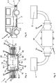
- FIG. 1 shows an inventive electronic unit 1 for a sensor 2 for a vehicle 3 in a first embodiment in a schematic view.
- the electronics unit 1 is shown without cover element 14, so that a housing body 12 of a housing 10 of the electronics unit 1 is shown open.
- the electronics unit 1 has on a first side 12. 1 of the housing 10 for connection to the vehicle 3 a first connection region 31 and for connection to the sensor 2 a second connection region 32 on a second side 12. 2 of the housing 10.
- the first and second side 12.1, 12.2 of the housing 10 with respect to the housing body 12 and / or a circuit board 20 against.
- the first and second sides 12.1, 12.2 of the housing 10 may include in particular sides of the housing body 12.
- first and the second connection region 31, 32 each preferably have at least one metallic contact region 35, on which an electrical connection of the electronics unit 1, in particular the printed circuit board 20, to the vehicle 3 or the sensor 2 can be produced.
- the contact regions 35 may have terminals through which an electrical connection to the electronics unit 1, in particular to the printed circuit board 20, can be produced.
- the contact areas 35 may also be part of a connector 40, for example.
- the printed circuit board 20 is further arranged in a cavity 11 of the housing 10.
- the cavity 11 is at least partially formed by the housing body 12.
- positioning aids 18 are also provided, which are formed as domes. As a result, a secure positioning of the printed circuit board 20 in the cavity 11 can be ensured.
- the positioning aids 18 are in particular provided integrally with the housing body 12.
- the printed circuit board 20 furthermore has a first circuit region 21, by means of which communication with the vehicle 3 can be processed, and a second circuit region 22, by which signals of the sensor 2 can be processed.
- the second circuit region 22 has a microcontroller for evaluating a measurement signal of the sensor 2.
- first and second circuit regions 21, 22 are arranged in rows on the printed circuit board 20, they have a large distance from each other.
- the first circuit region 21 has a smaller distance to the first connection region 31 for the vehicle 3 than the second circuit region 22.
- connecting elements 33 to the printed circuit board 20 each extend from the first and second connecting regions 31, 32.
- Four connecting elements 33 each extend from the first and second connecting regions 31, 32 to the printed circuit board 20.
- the connecting elements 33 protrude through openings of the printed circuit board 20 through the printed circuit board 20, so that an electrical connection can be ensured.
- a press-fit is provided for the connection of the printed circuit board 20 with the connecting elements 33.
- the printed circuit board 20 may further be cold-welded to the connecting elements 33. This results in a secure connection, which on the one hand can be mechanically and on the other hand electrically reliable.
- a potting compound 15 is also provided which at least partially fills the cavity 11.
- the potting compound 15 has a casting resin.
- the potting compound 15 completely fill the cavity 11, in particular when the cavity 11 is closed.
- the housing body 12 For mounting the electronics unit 1, the housing body 12 also has a housing opening 13, which is designed such that the printed circuit board 20 can be mounted in the cavity 11 through the housing opening 13. In particular, can when introducing the circuit board 20 into the cavity 11, the circuit board 20 with a side having circuit elements, be oriented parallel to a housing bottom.
- the housing 10 also has a first connection section 16 and a second connection section 17.
- the first and second connecting portions 16, 17 are formed integrally with the housing body 12.
- the first connection section 16 is assigned to the first connection region 31 and the second connection section 17 is assigned to the second connection region 32.
- the plug connectors 40 each extend at least partially into the connecting sections 16, 17 in order to be able to ensure secure fastening.
- the connecting portions 16, 17 extend from the housing body 12, a simple assembly of the connector 40 is possible.
- a mounting interface for standardized connectors 40 can be provided by the connecting sections.
- the housing body 12 has a length L of less than 150 mm, preferably less than 120 mm, more preferably less than 105 mm, a width B of less than 60 mm, preferably less than 50 mm and / or a height H of less than 25, preferably less than 20 mm, more preferably less than 15 mm.
- the electronics unit 1 can be within these dimensions, wherein, for example, the connectors 40 may be included.
- FIG. 2 shows the inventive electronic unit 1 of the first embodiment of FIG. 1 in a closed state.
- the housing opening 13 of the housing body 12 is closed with a cover element 14, so that the circuit board 20 is not accessible from the outside.
- the cover element 14 is integrally connected to the housing body 12, so that the cavity 11 can be sealed media-tight.
- the cover element 14 and / or the housing body 12 may preferably comprise a plastic, which is transparent to laser light.
- the cover element 14 and the housing body 12 may be laser-welded.
- FIG. 3 shows the electronic unit 1 according to the invention in a schematic, partially sectioned view of the first embodiment.
- the connecting elements 33 have a U-shaped bent portion 34.
- a first leg 34.1 of the bending section 34 is fastened to the printed circuit board 20 and a second leg 34.2 of the bent section 34 is fastened to the connecting section 16 or 17.
- the U-shaped bent section 34 is closed in the direction of a housing bottom 12.3 and in particular in the direction of the housing opening 13 open. This ensures that the first leg 34.1 each extends in the direction of the housing opening 13 and the circuit board 20 in a simple manner with the respective connecting element 33 is connectable.
- the positioning aids 18 each have a positioning shoulder 18.1, on which the printed circuit board 20 rests.
- connection regions 31, 32 can, as shown, lie parallel to one another in one plane or have an angle ⁇ to one another and / or to the printed circuit board 20.
- FIG. 4 further shows an inventive electronic unit 1 in a further embodiment in a schematic plan view in the open state.
- the electronics unit 1 has a first connection region 31 and a second connection region 32.
- the first terminal region 31 is configured to connect a printed circuit board 20 to a vehicle 3
- the second terminal region 32 is configured to connect the printed circuit board 20 to a sensor 2.
- the printed circuit board 20 is arranged between the terminal regions 31, 32, the terminal regions 31, 32 lying opposite one another with respect to the printed circuit board 20.
- the connection regions 31, 32 can have an angle ⁇ to one another and / or to the printed circuit board 20, for example.
- connecting elements 33 are provided which can ensure an electrical connection of the printed circuit board 20 to the outside.
- the connecting elements 33 may be metallic.
- the circuit board 20 is further in a cavity 11 of a housing 10th arranged, wherein the cavity 11 is at least partially formed by a housing body 12.
- positioning aids 18 are also provided, in particular, three positioning aids 18 are arranged such that the circuit board 20 can be correctly arranged only in exactly one orientation in the cavity 11.
- at least one of the positioning aids 18 is arranged irregularly, so that the printed circuit board 20 can not be mounted in the cavity 11 in an inverted orientation, for example.
- the printed circuit board 20 is arranged between the terminal regions 31, 32, so that a first circuit region 21, which is assigned to the first connection region for the vehicle, and a second circuit region 22, which is assigned to the second connection region 32 for the sensor 2, are arranged in a row.
- the housing 10 has attachment interfaces 19 for different attachment concepts. So shows FIG. 4 on the one hand fastening interfaces 19, which are designed as latching hooks, and on the other fastening interfaces 19, which have a fastening tab with a bore. Due to the different attachment interfaces 19, the electronics unit 1 can be adapted for a plurality of vehicle types, without it being necessary, for example, to individually adapt a casting tool for producing the housing 10.
- FIG. 5 further shows the inventive electronic unit 1 of the embodiment of FIG. 4
- the first connection region 31 is in this case connected to a vehicle electronics 4 of the vehicle 3, in particular a vehicle control device, and the second connection region 32 to the sensor 2.
- the sensor 2 may preferably be a foot switch for the vehicle Be 3.
- FIG. 6 further shows a vehicle according to the invention in a further embodiment.
- the vehicle has two electronic units 1, wherein one of the electronic units 1 is arranged in a side door 3.2 and a further electronic unit 1 of the electronic units is arranged in a bumper of the vehicle 3.
- Each of the electronic units 1 is connected to a sensor 2, which may preferably be designed as a footswitch.
- a sensor 2 which may preferably be designed as a footswitch.
- each of the electronic units 1 is connected to a vehicle electronics 4, which may preferably be a vehicle control unit.
- a vehicle electronics 4 which may preferably be a vehicle control unit.
- each of the electronic units 1 according to one of the embodiments of the FIGS. 1 to 5 educated.
- the electronic units 1 a connection possibility in the vehicle 3 is simplified and also a required space of the electronic units 1 is reduced.
- FIG. 7 further shows an inventive manufacturing method 100 for producing an electronics unit 1 for a sensor 2 for a vehicle 3 according to a further embodiment in a schematic representation of method steps.
- provision 101 of a first connection region 31 and a second connection region 32 is provided.
- the first connection region 31 serves for connecting the electronics unit 1 to the vehicle 3 and the second connection region 32 for connecting the electronics unit 1 to the sensor 2.
- Preferably at least partially simultaneously with the provision 101 of the first and second connection regions 31, 32 is an at least partial molding 102 of a housing 10 with a cavity 11 is provided.
- the molding 102 of the housing 10 preferably comprises that a housing body 12 is formed, which at least partially forms the cavity 11.
- a first connecting portion 16 and on a second side 12.1 of the housing 10 a second connecting portion 17 is integrally formed with the housing body 12 on a first side 12.1 of the housing 10.
- the molding 102 may be performed in a plastic injection molding process, such that the housing body 12 subsequently comprises a plastic and is molded during molding 102 around connecting elements 33 and / or contact areas 35 of the first and / or second terminal areas 31, 32.
- placing 103 of the printed circuit board 20 between the first and second terminal regions 31, 32 in the cavity 11 is provided.
- the arrangement 103 of the printed circuit board 20 in the cavity 11 preferably takes place through a housing opening 13 of the housing body 12, wherein the housing opening 13 is closed by a cover element 14 after arranging the conductor lath 20 in the cavity 11.
- the circuit board 20 is moved during the introduction into the cavity 11 in a direction perpendicular to a housing bottom 12.3 of the housing body 12.
- an at least partial filling 104 of the cavity 11 is provided with a potting compound 15, so that the printed circuit board 20 is potted with the potting compound 15.
- the manufacturing method 100 comprises a closure 105 of the cavity 11 with a cover element 14.
- the cover element 14 is connected to the housing body 12 in a material-locking manner, preferably laser-welded.
- a particularly secure connection can be ensured, in particular, with a seal.
Landscapes
- Engineering & Computer Science (AREA)
- Microelectronics & Electronic Packaging (AREA)
- Casings For Electric Apparatus (AREA)
Applications Claiming Priority (1)
| Application Number | Priority Date | Filing Date | Title |
|---|---|---|---|
| DE102017115047.1A DE102017115047A1 (de) | 2017-07-05 | 2017-07-05 | Elektronikeinheit für einen Sensor, Fahrzeug sowie Herstellverfahren zum Herstellen einer Elektronikeinheit |
Publications (2)
| Publication Number | Publication Date |
|---|---|
| EP3426011A1 true EP3426011A1 (fr) | 2019-01-09 |
| EP3426011B1 EP3426011B1 (fr) | 2022-02-16 |
Family
ID=62846079
Family Applications (1)
| Application Number | Title | Priority Date | Filing Date |
|---|---|---|---|
| EP18181504.4A Active EP3426011B1 (fr) | 2017-07-05 | 2018-07-03 | Unité électronique pour un capteur, véhicule ainsi que procédé de fabrication d'une unit é électronique |
Country Status (3)
| Country | Link |
|---|---|
| EP (1) | EP3426011B1 (fr) |
| CN (1) | CN109219284A (fr) |
| DE (1) | DE102017115047A1 (fr) |
Families Citing this family (1)
| Publication number | Priority date | Publication date | Assignee | Title |
|---|---|---|---|---|
| DE102019210375A1 (de) * | 2019-07-12 | 2021-01-14 | Continental Teves Ag & Co. Ohg | Verfahren zur Herstellung eines robusten Sensors |
Citations (3)
| Publication number | Priority date | Publication date | Assignee | Title |
|---|---|---|---|---|
| US6068491A (en) * | 1996-12-06 | 2000-05-30 | Robert Bosch Gmbh | Connector arrangement for an automotive steering system with a control unit |
| EP1689058A1 (fr) * | 2003-11-18 | 2006-08-09 | Hitachi, Ltd. | Module de commande |
| WO2015028254A1 (fr) * | 2013-08-30 | 2015-03-05 | Robert Bosch Gmbh | Nouveau type de connexion d'un circuit imprimé souple au boîtier d'un appareil de commande |
Family Cites Families (6)
| Publication number | Priority date | Publication date | Assignee | Title |
|---|---|---|---|---|
| JPH02170597A (ja) * | 1988-12-23 | 1990-07-02 | Mazda Motor Corp | 車載用制御ユニツト構造 |
| JP2000315873A (ja) * | 1999-04-28 | 2000-11-14 | Matsushita Electric Ind Co Ltd | 組み込み型電子機器 |
| BRMU8900643Y1 (pt) * | 2009-04-17 | 2017-04-25 | Robert Bosch Ltda | alojamento para a eletrônica de comando de um motor de corrente contínua sem escovas |
| JP2011096636A (ja) * | 2009-09-30 | 2011-05-12 | Sanyo Electric Co Ltd | 回路モジュールおよびそれを備えた電動車両 |
| DE102011088969A1 (de) * | 2011-12-19 | 2013-06-20 | Robert Bosch Gmbh | Getriebesteuermodul |
| DE102012207599B4 (de) * | 2012-05-08 | 2022-03-17 | Vitesco Technologies GmbH | Steuergerät, insbesondere für ein Kraftfahrzeug |
-
2017
- 2017-07-05 DE DE102017115047.1A patent/DE102017115047A1/de not_active Withdrawn
-
2018
- 2018-06-29 CN CN201810699399.5A patent/CN109219284A/zh active Pending
- 2018-07-03 EP EP18181504.4A patent/EP3426011B1/fr active Active
Patent Citations (3)
| Publication number | Priority date | Publication date | Assignee | Title |
|---|---|---|---|---|
| US6068491A (en) * | 1996-12-06 | 2000-05-30 | Robert Bosch Gmbh | Connector arrangement for an automotive steering system with a control unit |
| EP1689058A1 (fr) * | 2003-11-18 | 2006-08-09 | Hitachi, Ltd. | Module de commande |
| WO2015028254A1 (fr) * | 2013-08-30 | 2015-03-05 | Robert Bosch Gmbh | Nouveau type de connexion d'un circuit imprimé souple au boîtier d'un appareil de commande |
Also Published As
| Publication number | Publication date |
|---|---|
| CN109219284A (zh) | 2019-01-15 |
| DE102017115047A1 (de) | 2019-01-10 |
| EP3426011B1 (fr) | 2022-02-16 |
Similar Documents
| Publication | Publication Date | Title |
|---|---|---|
| DE102013206443B4 (de) | System aus einem Gehäuse und einem Stecker für eine automatisierte, maschinelle Kabelbaumdirektmontage, wobei das System zwei Dichtmittel und zwei Verriegelungsmittel zur irreversiblen Verriegelung umfasst und zugehöriges Herstellungsverfahren | |
| DE19936300A1 (de) | Druckerkennungsvorrichtung, Verbindungsteil hierfür, sowie Verfahren zur Herstellung eines elektrischen Bauteileverbinders | |
| EP3507437B1 (fr) | Module électronique pour système de poignée de porte de véhicule automobile | |
| DE19755767C2 (de) | Gehäuse mit Steckereinheit | |
| EP3679211B1 (fr) | Ensemble formant poignée de portière de véhicule automobile intégrant un système électronique scellé | |
| EP0984121A2 (fr) | Actionneur | |
| EP3507862B1 (fr) | Dispositif de poignée de porte de véhicule à moteur comprenant un espace de montage électronique étanche | |
| EP3507861A1 (fr) | Dispositif de poignée de porte de véhicule à moteur doté d'un système pour faciliter le montage | |
| EP1608994B1 (fr) | Ensemble capteur d'un systeme d'aide au stationnement | |
| DE112010003624T5 (de) | Gehäusebauteil für eine Türschlossbaugruppe und Verfahren zu deren Herstellung | |
| DE19848081A1 (de) | Antriebseinrichtung mit einem Stellantrieb | |
| DE102005040169A1 (de) | Höhenvariabel einbaubarer Drehzahlsensor | |
| EP3426011B1 (fr) | Unité électronique pour un capteur, véhicule ainsi que procédé de fabrication d'une unit é électronique | |
| EP4248042B1 (fr) | Ensemble électronique destiné aux portières ou volets de véhicule automobile | |
| DE102011003239B4 (de) | Sensormodul, Montageelement und Verfahren zum Herstellen eines Sensormoduls | |
| EP3507438A1 (fr) | Ensemble poignée de porte de véhicule à moteur doté d'une antenne | |
| DE102018111007A1 (de) | Griffkörper für einen Türgriff | |
| EP3507439B1 (fr) | Ensemble poignée de porte de véhicule à moteur doté d'un connecteur fixé par complémentarité de forme | |
| DE102017219891A1 (de) | Umspritzverfahren für eine Sensoreinheit | |
| WO2018046176A1 (fr) | Poignée de porte de véhicule | |
| DE102005042248B3 (de) | Formbauteil für ein Kraftfahrzeug und Verfahren zu dessen Herstellung | |
| WO2018046051A1 (fr) | Support de composants pour composants électriques/électroniques, destiné à se monter dans une serrure de porte de véhicule automobile | |
| DE8816054U1 (de) | Elektrisches Gerät | |
| DE102022110010A1 (de) | Massekontaktmodul für ein Steuergerät sowie Steuergerät und Montageverfahren | |
| DE102024111023A1 (de) | Kraftfahrzeug-Schlosseinheit |
Legal Events
| Date | Code | Title | Description |
|---|---|---|---|
| PUAI | Public reference made under article 153(3) epc to a published international application that has entered the european phase |
Free format text: ORIGINAL CODE: 0009012 |
|
| STAA | Information on the status of an ep patent application or granted ep patent |
Free format text: STATUS: THE APPLICATION HAS BEEN PUBLISHED |
|
| AK | Designated contracting states |
Kind code of ref document: A1 Designated state(s): AL AT BE BG CH CY CZ DE DK EE ES FI FR GB GR HR HU IE IS IT LI LT LU LV MC MK MT NL NO PL PT RO RS SE SI SK SM TR |
|
| AX | Request for extension of the european patent |
Extension state: BA ME |
|
| STAA | Information on the status of an ep patent application or granted ep patent |
Free format text: STATUS: REQUEST FOR EXAMINATION WAS MADE |
|
| 17P | Request for examination filed |
Effective date: 20190709 |
|
| RBV | Designated contracting states (corrected) |
Designated state(s): AL AT BE BG CH CY CZ DE DK EE ES FI FR GB GR HR HU IE IS IT LI LT LU LV MC MK MT NL NO PL PT RO RS SE SI SK SM TR |
|
| STAA | Information on the status of an ep patent application or granted ep patent |
Free format text: STATUS: EXAMINATION IS IN PROGRESS |
|
| 17Q | First examination report despatched |
Effective date: 20210222 |
|
| GRAP | Despatch of communication of intention to grant a patent |
Free format text: ORIGINAL CODE: EPIDOSNIGR1 |
|
| STAA | Information on the status of an ep patent application or granted ep patent |
Free format text: STATUS: GRANT OF PATENT IS INTENDED |
|
| INTG | Intention to grant announced |
Effective date: 20211122 |
|
| GRAS | Grant fee paid |
Free format text: ORIGINAL CODE: EPIDOSNIGR3 |
|
| GRAA | (expected) grant |
Free format text: ORIGINAL CODE: 0009210 |
|
| STAA | Information on the status of an ep patent application or granted ep patent |
Free format text: STATUS: THE PATENT HAS BEEN GRANTED |
|
| AK | Designated contracting states |
Kind code of ref document: B1 Designated state(s): AL AT BE BG CH CY CZ DE DK EE ES FI FR GB GR HR HU IE IS IT LI LT LU LV MC MK MT NL NO PL PT RO RS SE SI SK SM TR |
|
| REG | Reference to a national code |
Ref country code: GB Ref legal event code: FG4D Free format text: NOT ENGLISH |
|
| REG | Reference to a national code |
Ref country code: CH Ref legal event code: EP |
|
| REG | Reference to a national code |
Ref country code: DE Ref legal event code: R096 Ref document number: 502018008773 Country of ref document: DE |
|
| REG | Reference to a national code |
Ref country code: AT Ref legal event code: REF Ref document number: 1469720 Country of ref document: AT Kind code of ref document: T Effective date: 20220315 |
|
| REG | Reference to a national code |
Ref country code: IE Ref legal event code: FG4D Free format text: LANGUAGE OF EP DOCUMENT: GERMAN |
|
| REG | Reference to a national code |
Ref country code: LT Ref legal event code: MG9D |
|
| REG | Reference to a national code |
Ref country code: NL Ref legal event code: MP Effective date: 20220216 |
|
| PG25 | Lapsed in a contracting state [announced via postgrant information from national office to epo] |
Ref country code: SE Free format text: LAPSE BECAUSE OF FAILURE TO SUBMIT A TRANSLATION OF THE DESCRIPTION OR TO PAY THE FEE WITHIN THE PRESCRIBED TIME-LIMIT Effective date: 20220216 Ref country code: RS Free format text: LAPSE BECAUSE OF FAILURE TO SUBMIT A TRANSLATION OF THE DESCRIPTION OR TO PAY THE FEE WITHIN THE PRESCRIBED TIME-LIMIT Effective date: 20220216 Ref country code: PT Free format text: LAPSE BECAUSE OF FAILURE TO SUBMIT A TRANSLATION OF THE DESCRIPTION OR TO PAY THE FEE WITHIN THE PRESCRIBED TIME-LIMIT Effective date: 20220616 Ref country code: NO Free format text: LAPSE BECAUSE OF FAILURE TO SUBMIT A TRANSLATION OF THE DESCRIPTION OR TO PAY THE FEE WITHIN THE PRESCRIBED TIME-LIMIT Effective date: 20220516 Ref country code: NL Free format text: LAPSE BECAUSE OF FAILURE TO SUBMIT A TRANSLATION OF THE DESCRIPTION OR TO PAY THE FEE WITHIN THE PRESCRIBED TIME-LIMIT Effective date: 20220216 Ref country code: LT Free format text: LAPSE BECAUSE OF FAILURE TO SUBMIT A TRANSLATION OF THE DESCRIPTION OR TO PAY THE FEE WITHIN THE PRESCRIBED TIME-LIMIT Effective date: 20220216 Ref country code: HR Free format text: LAPSE BECAUSE OF FAILURE TO SUBMIT A TRANSLATION OF THE DESCRIPTION OR TO PAY THE FEE WITHIN THE PRESCRIBED TIME-LIMIT Effective date: 20220216 Ref country code: ES Free format text: LAPSE BECAUSE OF FAILURE TO SUBMIT A TRANSLATION OF THE DESCRIPTION OR TO PAY THE FEE WITHIN THE PRESCRIBED TIME-LIMIT Effective date: 20220216 Ref country code: BG Free format text: LAPSE BECAUSE OF FAILURE TO SUBMIT A TRANSLATION OF THE DESCRIPTION OR TO PAY THE FEE WITHIN THE PRESCRIBED TIME-LIMIT Effective date: 20220516 |
|
| PG25 | Lapsed in a contracting state [announced via postgrant information from national office to epo] |
Ref country code: PL Free format text: LAPSE BECAUSE OF FAILURE TO SUBMIT A TRANSLATION OF THE DESCRIPTION OR TO PAY THE FEE WITHIN THE PRESCRIBED TIME-LIMIT Effective date: 20220216 Ref country code: LV Free format text: LAPSE BECAUSE OF FAILURE TO SUBMIT A TRANSLATION OF THE DESCRIPTION OR TO PAY THE FEE WITHIN THE PRESCRIBED TIME-LIMIT Effective date: 20220216 Ref country code: GR Free format text: LAPSE BECAUSE OF FAILURE TO SUBMIT A TRANSLATION OF THE DESCRIPTION OR TO PAY THE FEE WITHIN THE PRESCRIBED TIME-LIMIT Effective date: 20220517 Ref country code: FI Free format text: LAPSE BECAUSE OF FAILURE TO SUBMIT A TRANSLATION OF THE DESCRIPTION OR TO PAY THE FEE WITHIN THE PRESCRIBED TIME-LIMIT Effective date: 20220216 |
|
| PG25 | Lapsed in a contracting state [announced via postgrant information from national office to epo] |
Ref country code: IS Free format text: LAPSE BECAUSE OF FAILURE TO SUBMIT A TRANSLATION OF THE DESCRIPTION OR TO PAY THE FEE WITHIN THE PRESCRIBED TIME-LIMIT Effective date: 20220617 |
|
| PG25 | Lapsed in a contracting state [announced via postgrant information from national office to epo] |
Ref country code: SM Free format text: LAPSE BECAUSE OF FAILURE TO SUBMIT A TRANSLATION OF THE DESCRIPTION OR TO PAY THE FEE WITHIN THE PRESCRIBED TIME-LIMIT Effective date: 20220216 Ref country code: SK Free format text: LAPSE BECAUSE OF FAILURE TO SUBMIT A TRANSLATION OF THE DESCRIPTION OR TO PAY THE FEE WITHIN THE PRESCRIBED TIME-LIMIT Effective date: 20220216 Ref country code: RO Free format text: LAPSE BECAUSE OF FAILURE TO SUBMIT A TRANSLATION OF THE DESCRIPTION OR TO PAY THE FEE WITHIN THE PRESCRIBED TIME-LIMIT Effective date: 20220216 Ref country code: EE Free format text: LAPSE BECAUSE OF FAILURE TO SUBMIT A TRANSLATION OF THE DESCRIPTION OR TO PAY THE FEE WITHIN THE PRESCRIBED TIME-LIMIT Effective date: 20220216 Ref country code: DK Free format text: LAPSE BECAUSE OF FAILURE TO SUBMIT A TRANSLATION OF THE DESCRIPTION OR TO PAY THE FEE WITHIN THE PRESCRIBED TIME-LIMIT Effective date: 20220216 Ref country code: CZ Free format text: LAPSE BECAUSE OF FAILURE TO SUBMIT A TRANSLATION OF THE DESCRIPTION OR TO PAY THE FEE WITHIN THE PRESCRIBED TIME-LIMIT Effective date: 20220216 |
|
| REG | Reference to a national code |
Ref country code: DE Ref legal event code: R097 Ref document number: 502018008773 Country of ref document: DE |
|
| PG25 | Lapsed in a contracting state [announced via postgrant information from national office to epo] |
Ref country code: AL Free format text: LAPSE BECAUSE OF FAILURE TO SUBMIT A TRANSLATION OF THE DESCRIPTION OR TO PAY THE FEE WITHIN THE PRESCRIBED TIME-LIMIT Effective date: 20220216 |
|
| PLBE | No opposition filed within time limit |
Free format text: ORIGINAL CODE: 0009261 |
|
| STAA | Information on the status of an ep patent application or granted ep patent |
Free format text: STATUS: NO OPPOSITION FILED WITHIN TIME LIMIT |
|
| 26N | No opposition filed |
Effective date: 20221117 |
|
| PG25 | Lapsed in a contracting state [announced via postgrant information from national office to epo] |
Ref country code: SI Free format text: LAPSE BECAUSE OF FAILURE TO SUBMIT A TRANSLATION OF THE DESCRIPTION OR TO PAY THE FEE WITHIN THE PRESCRIBED TIME-LIMIT Effective date: 20220216 Ref country code: MC Free format text: LAPSE BECAUSE OF FAILURE TO SUBMIT A TRANSLATION OF THE DESCRIPTION OR TO PAY THE FEE WITHIN THE PRESCRIBED TIME-LIMIT Effective date: 20220216 |
|
| REG | Reference to a national code |
Ref country code: CH Ref legal event code: PL |
|
| REG | Reference to a national code |
Ref country code: BE Ref legal event code: MM Effective date: 20220731 |
|
| PG25 | Lapsed in a contracting state [announced via postgrant information from national office to epo] |
Ref country code: LU Free format text: LAPSE BECAUSE OF NON-PAYMENT OF DUE FEES Effective date: 20220703 Ref country code: LI Free format text: LAPSE BECAUSE OF NON-PAYMENT OF DUE FEES Effective date: 20220731 Ref country code: CH Free format text: LAPSE BECAUSE OF NON-PAYMENT OF DUE FEES Effective date: 20220731 |
|
| PG25 | Lapsed in a contracting state [announced via postgrant information from national office to epo] |
Ref country code: BE Free format text: LAPSE BECAUSE OF NON-PAYMENT OF DUE FEES Effective date: 20220731 |
|
| P01 | Opt-out of the competence of the unified patent court (upc) registered |
Effective date: 20230427 |
|
| PG25 | Lapsed in a contracting state [announced via postgrant information from national office to epo] |
Ref country code: IT Free format text: LAPSE BECAUSE OF FAILURE TO SUBMIT A TRANSLATION OF THE DESCRIPTION OR TO PAY THE FEE WITHIN THE PRESCRIBED TIME-LIMIT Effective date: 20220216 Ref country code: IE Free format text: LAPSE BECAUSE OF NON-PAYMENT OF DUE FEES Effective date: 20220703 |
|
| PG25 | Lapsed in a contracting state [announced via postgrant information from national office to epo] |
Ref country code: HU Free format text: LAPSE BECAUSE OF FAILURE TO SUBMIT A TRANSLATION OF THE DESCRIPTION OR TO PAY THE FEE WITHIN THE PRESCRIBED TIME-LIMIT; INVALID AB INITIO Effective date: 20180703 |
|
| PG25 | Lapsed in a contracting state [announced via postgrant information from national office to epo] |
Ref country code: MK Free format text: LAPSE BECAUSE OF FAILURE TO SUBMIT A TRANSLATION OF THE DESCRIPTION OR TO PAY THE FEE WITHIN THE PRESCRIBED TIME-LIMIT Effective date: 20220216 Ref country code: CY Free format text: LAPSE BECAUSE OF FAILURE TO SUBMIT A TRANSLATION OF THE DESCRIPTION OR TO PAY THE FEE WITHIN THE PRESCRIBED TIME-LIMIT Effective date: 20220216 |
|
| REG | Reference to a national code |
Ref country code: AT Ref legal event code: MM01 Ref document number: 1469720 Country of ref document: AT Kind code of ref document: T Effective date: 20230703 |
|
| PG25 | Lapsed in a contracting state [announced via postgrant information from national office to epo] |
Ref country code: MT Free format text: LAPSE BECAUSE OF FAILURE TO SUBMIT A TRANSLATION OF THE DESCRIPTION OR TO PAY THE FEE WITHIN THE PRESCRIBED TIME-LIMIT Effective date: 20220216 |
|
| PG25 | Lapsed in a contracting state [announced via postgrant information from national office to epo] |
Ref country code: AT Free format text: LAPSE BECAUSE OF NON-PAYMENT OF DUE FEES Effective date: 20230703 |
|
| PG25 | Lapsed in a contracting state [announced via postgrant information from national office to epo] |
Ref country code: AT Free format text: LAPSE BECAUSE OF NON-PAYMENT OF DUE FEES Effective date: 20230703 |
|
| PGFP | Annual fee paid to national office [announced via postgrant information from national office to epo] |
Ref country code: DE Payment date: 20250731 Year of fee payment: 8 |
|
| PGFP | Annual fee paid to national office [announced via postgrant information from national office to epo] |
Ref country code: GB Payment date: 20250724 Year of fee payment: 8 |
|
| PGFP | Annual fee paid to national office [announced via postgrant information from national office to epo] |
Ref country code: FR Payment date: 20250723 Year of fee payment: 8 |
|
| PG25 | Lapsed in a contracting state [announced via postgrant information from national office to epo] |
Ref country code: TR Free format text: LAPSE BECAUSE OF FAILURE TO SUBMIT A TRANSLATION OF THE DESCRIPTION OR TO PAY THE FEE WITHIN THE PRESCRIBED TIME-LIMIT Effective date: 20220216 |
|
| PGFP | Annual fee paid to national office [announced via postgrant information from national office to epo] |
Ref country code: AT Payment date: 20260410 Year of fee payment: 5 |