EP3450947B1 - Spannungssensor für halbleiterbauelemente - Google Patents
Spannungssensor für halbleiterbauelemente Download PDFInfo
- Publication number
- EP3450947B1 EP3450947B1 EP17189517.0A EP17189517A EP3450947B1 EP 3450947 B1 EP3450947 B1 EP 3450947B1 EP 17189517 A EP17189517 A EP 17189517A EP 3450947 B1 EP3450947 B1 EP 3450947B1
- Authority
- EP
- European Patent Office
- Prior art keywords
- slanted
- paths
- resistive
- cavity
- substrate
- Prior art date
- Legal status (The legal status is an assumption and is not a legal conclusion. Google has not performed a legal analysis and makes no representation as to the accuracy of the status listed.)
- Active
Links
Images


Classifications
-
- G—PHYSICS
- G01—MEASURING; TESTING
- G01L—MEASURING FORCE, STRESS, TORQUE, WORK, MECHANICAL POWER, MECHANICAL EFFICIENCY, OR FLUID PRESSURE
- G01L5/00—Apparatus for, or methods of, measuring force, work, mechanical power, or torque, specially adapted for specific purposes
- G01L5/16—Apparatus for, or methods of, measuring force, work, mechanical power, or torque, specially adapted for specific purposes for measuring several components of force
- G01L5/161—Apparatus for, or methods of, measuring force, work, mechanical power, or torque, specially adapted for specific purposes for measuring several components of force using variations in ohmic resistance
- G01L5/162—Apparatus for, or methods of, measuring force, work, mechanical power, or torque, specially adapted for specific purposes for measuring several components of force using variations in ohmic resistance of piezoresistors
-
- G—PHYSICS
- G01—MEASURING; TESTING
- G01L—MEASURING FORCE, STRESS, TORQUE, WORK, MECHANICAL POWER, MECHANICAL EFFICIENCY, OR FLUID PRESSURE
- G01L1/00—Measuring force or stress, in general
- G01L1/16—Measuring force or stress, in general using properties of piezoelectric devices
-
- G—PHYSICS
- G01—MEASURING; TESTING
- G01L—MEASURING FORCE, STRESS, TORQUE, WORK, MECHANICAL POWER, MECHANICAL EFFICIENCY, OR FLUID PRESSURE
- G01L1/00—Measuring force or stress, in general
- G01L1/18—Measuring force or stress, in general using properties of piezo-resistive materials, i.e. materials of which the ohmic resistance varies according to changes in magnitude or direction of force applied to the material
-
- G—PHYSICS
- G01—MEASURING; TESTING
- G01L—MEASURING FORCE, STRESS, TORQUE, WORK, MECHANICAL POWER, MECHANICAL EFFICIENCY, OR FLUID PRESSURE
- G01L1/00—Measuring force or stress, in general
- G01L1/20—Measuring force or stress, in general by measuring variations in ohmic resistance of solid materials or of electrically-conductive fluids; by making use of electrokinetic cells, i.e. liquid-containing cells wherein an electrical potential is produced or varied upon the application of stress
- G01L1/22—Measuring force or stress, in general by measuring variations in ohmic resistance of solid materials or of electrically-conductive fluids; by making use of electrokinetic cells, i.e. liquid-containing cells wherein an electrical potential is produced or varied upon the application of stress using resistance strain gauges
- G01L1/2287—Measuring force or stress, in general by measuring variations in ohmic resistance of solid materials or of electrically-conductive fluids; by making use of electrokinetic cells, i.e. liquid-containing cells wherein an electrical potential is produced or varied upon the application of stress using resistance strain gauges constructional details of the strain gauges
- G01L1/2293—Measuring force or stress, in general by measuring variations in ohmic resistance of solid materials or of electrically-conductive fluids; by making use of electrokinetic cells, i.e. liquid-containing cells wherein an electrical potential is produced or varied upon the application of stress using resistance strain gauges constructional details of the strain gauges of the semi-conductor type
-
- H—ELECTRICITY
- H10—SEMICONDUCTOR DEVICES; ELECTRIC SOLID-STATE DEVICES NOT OTHERWISE PROVIDED FOR
- H10P—GENERIC PROCESSES OR APPARATUS FOR THE MANUFACTURE OR TREATMENT OF DEVICES COVERED BY CLASS H10
- H10P30/00—Ion implantation into wafers, substrates or parts of devices
- H10P30/20—Ion implantation into wafers, substrates or parts of devices into semiconductor materials, e.g. for doping
- H10P30/202—Ion implantation into wafers, substrates or parts of devices into semiconductor materials, e.g. for doping characterised by the semiconductor materials
- H10P30/204—Ion implantation into wafers, substrates or parts of devices into semiconductor materials, e.g. for doping characterised by the semiconductor materials into Group IV semiconductors
-
- H—ELECTRICITY
- H10—SEMICONDUCTOR DEVICES; ELECTRIC SOLID-STATE DEVICES NOT OTHERWISE PROVIDED FOR
- H10P—GENERIC PROCESSES OR APPARATUS FOR THE MANUFACTURE OR TREATMENT OF DEVICES COVERED BY CLASS H10
- H10P30/00—Ion implantation into wafers, substrates or parts of devices
- H10P30/20—Ion implantation into wafers, substrates or parts of devices into semiconductor materials, e.g. for doping
- H10P30/21—Ion implantation into wafers, substrates or parts of devices into semiconductor materials, e.g. for doping of electrically active species
-
- H—ELECTRICITY
- H10—SEMICONDUCTOR DEVICES; ELECTRIC SOLID-STATE DEVICES NOT OTHERWISE PROVIDED FOR
- H10P—GENERIC PROCESSES OR APPARATUS FOR THE MANUFACTURE OR TREATMENT OF DEVICES COVERED BY CLASS H10
- H10P74/00—Testing or measuring during manufacture or treatment of wafers, substrates or devices
- H10P74/27—Structural arrangements therefor
- H10P74/273—Interconnections for measuring or testing, e.g. probe pads
Definitions
- the present invention is related to a stress sensor integrated in a semiconductor component such as an integrated circuit chip.
- a well-known approach to detecting package-induced stress is based on the piezoresistive effect in diffused resistors or transistors.
- a piezo-resistive stress sensor built on this principle is the rosette sensor described in detail in document " Silicon piezoresistive stress sensors and their application in electronic packaging," Suhling and Jaeger, IEEE Sensors Journal, vol. 1, no. 1, pp. 14-30, June 2001 .
- the shift in resistance of complementary type diffused resistors oriented along different directions is monitored to deduce the stress present in the active material. To compensate for the impact of temperature variations during measurements, these resistance shifts must be subtracted one from the other so as to cancel the impact of thermal effects on resistors.
- one approach is to build rosette sensors on a (111) surface, where the transformed piezoresistive matrix provides more orientation-dependent coefficients. Therefore, variations of resistances oriented in different directions due to stress have the potential to provide an independent family of linear equations from which the stress components can be extracted. Nonetheless, the in-plane resistivity matrix being symmetric, it features only 3 independent components. Any in-plane rotation of the resistor can only result in a combination of these three coefficients. Thus at most 3 independent equations can be extracted from a single-polarity rosette sensor, and one is inevitably lost for temperature compensation. In any case, all the sensors based on a (111) surface cannot be processed in conventional CMOS technology where the wafer surface is oriented along the (100) direction.
- V-groove stress sensors are a well-known technique used in the MEMS industry to fabricate sensors. In particular, it has also been used to build membrane sensors that can detect a pressure applied by an external force on the chip. However in that case the V-groove is used simply to build a mechanical structure. The electrical characteristics of the resulting slanted surfaces are not exploited. For example in document US6150681 , the piezoresistive sensors are put on the membrane and not on the slanted surfaces themselves. Furthermore, all piezoresistive sensors relying on a free membrane or an internal cavity are not suitable for detecting packaging-induced stress precisely because they are sensitive to the external stress (which they are meant to detect).
- Document FR2950427 is related to a sensor having an electromechanical microsystem including a single-crystal silicon substrate with a central active zone on which piezo-resistive gauges i.e. beams, are interconnected to form a Wheatstone bridge.
- the substrate includes active zones on which an electrical conditioning circuit for amplifying and transmitting an output signal of the bridge is integrated.
- Power supply units generate supply current from mechanical deformation of a structure measured by the piezo-resistive gauges, to supply the current to the microsystem and include a bar.
- the bar is made of piezoelectric material i.e. lithium niobate single crystal.
- Document WO02/44655 is related to a three-axis sensor assembly for use in an elastomeric material including a first pair of sensors disposed along a first pair of respective planes that intersect, the first sensors being adapted to detect a force in a first direction.
- the sensor assembly includes a second pair of sensors disposed along a second pair of respective planes that intersect, the second sensors detecting a force in a second direction generally orthogonal to the first direction.
- the elastomeric material can be a vehicle tire, and the tire may include a plurality of the sensor assemblies disposed about its perimeter in mutually spaced relationship.
- Document US2009/282930 is related to a force sensor including a polymeric substrate including a cavity with a tilt plane, at least two metal piezoresistors on the tilt plane, and a contact pad connected to the metal piezoresistors.
- the tilt plane may include a measured interface of from 15° to 75°.
- Document US2015/059486 is related to a pressure sensor including an elastic thin film including a first surface and a second surface that face each other, the elastic thin film including an elastomer material, a plurality of protruding deformable structures patterned on the first surface, a piezoresistive electrode formed along surfaces of the plurality of protruding deformable structures and a counter electrode disposed to face the piezoresistive electrode.
- Document EP1380825 is related to a micromechanical pressure sensor having a part silicon semiconductor frame holding a membrane with stress dependent Wheatstone bridge and compensation bridge piezo resistances having part linear and part quadratic responses on the membrane and others optionally on the frame.
- the invention is related to a sensor and to a semiconductor component in accordance with the appended claims.
- the sensor of the invention is configured to be incorporated in a semiconductor component such as an integrated circuit chip.
- the component comprises a semiconductor substrate, the substrate originating from the semiconductor wafer onto which a plurality of chips are built.
- a stress sensor according to the present invention comprises one or more slanted surfaces of the semiconductor substrate material with a known oblique inclination angle relative to the main surface of the substrate, and resistive paths at least on the slanted surfaces.
- two slanted surfaces are provided with complementary inclination angles relative to the main surface, and one or more pairs of resistive paths are produced on the pair of surfaces, the inclination angles of the paths of each pair being equally complementary.
- the knowledge of the inclination angle allows to determine the out-of-plane stress components based on a measurement of the resistance of the slanted resistive paths.
- the sensor may comprise a cavity open to the main surface, or a 3D shape on the main surface, and a number of resistive paths on the slanted sidewalls of the cavity or 3D-shape, as well as a number of contacts and terminals for accessing said resistive paths.
- the sensor further comprises planar resistive paths in the vicinity of the cavity or 3D shape, which allow to determine the normal stress components, as well as the in-plane shear stress.
- the sensor according to the invention provides a way of monitoring or determining the out-of-plane shear stress that is technically straightforward and reliable in comparison with the existing approaches referred to above.
- the invention is firstly related to a sensor for monitoring and/or measuring stress in the semiconductor component, the stress sensor comprising a substrate formed of a piezoresistive semiconductor material, the substrate comprising a planar main surface, the sensor comprising :
- the senor comprises at least one pair of slanted surfaces having complementary inclination angles relative to the main surface, and comprising at least one pair of resistive paths which lie in a first plane, the first path on the first slanted surface and the second path on the second slanted surface, wherein the pair of slanted resistive paths also have complementary inclination angles relative to the main surface, and wherein the sensor is configured to measure the shear stress in the first plane defined by the pair of resistive paths.
- the sensor may comprise two of said pairs of slanted surfaces and slanted resistive paths, and be configured to measure the shear stress in a first and second plane, said planes being two mutually non-parallel planes, preferably two mutually orthogonal planes.
- the senor further comprises a plurality of planar resistive paths parallel to the plane of the main surface of the substrate and located in the vicinity of the slanted resistive paths, as well as a plurality of contacts and terminals for accessing the planar resistive paths, thereby allowing to measure the electrical resistance of the planar paths and to derive therefrom an assessment of one or more additional stress components.
- the one or more slanted surfaces are the slanted sidewalls of one or more cavities which are open to the main surface of the substrate or to another surface of the substrate and/or the slanted surfaces are the slanted sidewalls of 3-dimensional shapes extending outward from the main surface of the substrate or from another surface of the substrate.
- the senor comprises :
- the sensor according to the previous paragraph may further comprise a fifth electrical contact located in the tip area, the four resistive paths extending respectively between the four contacts and the fifth contact.
- the four slanted resistive paths merge in the tip area and the slanted resistive paths on opposing walls of the cavity or the 3D shape are matched in terms of their electric resistance.
- the sensor comprising a pyramid-shaped cavity or 3D shape as described above may further comprise :
- the sensor according to the preceding paragraph may further comprise two additional planar resistive paths, as well as contacts at the start and end location of each additional planar path, wherein :
- the two pairs of parallel resistive paths may form the side edges of a rectangle, with four contacts placed on the corners of the rectangle.
- the sensor comprising a pyramid-shaped cavity or 3D shape may further comprise :
- the substrate material is a crystalline semiconductor material, and the inclination angles are defined by the crystallographic structure of the material.
- the senor comprises multiple resistive paths obtained by implantation of dopant elements in narrow areas of the slanted surfaces, and, if applicable, in narrow areas of the main surface of the substrate or a surface parallel thereto, and wherein the sensor comprises resistive paths formed by implantation of dopant elements of a first polarity type, as well as resistive paths formed by implantation of dopant elements of a second polarity type, opposite to the first.
- the invention is equally relatedt to a semiconductor component comprising a stress sensor in accordance with the invention.
- a stress sensor is formed on a semiconductor substrate having a planar main surface, wherein the sensor comprises at least one slanted surface of the substrate material, 'slanted' meaning that the surface is a flat surface oriented at an oblique angle relative to the main surface, and on said slanted surface at least one resistive path.
- the semiconductor material is preferably a piezoresistive material, more preferably a piezoresistive crystalline material, for example silicon, germanium or a compound semiconductor (e.g. GaAs).
- the path is slanted as a consequence of the oblique inclination angle of the surface.
- a 'resistive path' is defined within the present context as a portion of the surface that is equivalent to a one-dimensional conductor and which is thus characterised by a measurable electrical resistance.
- the resistive path As the resistive path is one-dimensional, it has a well-defined inclination angle relative to the main surface of the substrate. The resistive path is thus straight relative to the slanted surface. Any oblique (i.e. different from 90°) inclination angle may be applied between the resistive path and the main surface of the substrate. According to a preferred embodiment, the angle is between 20° and 70°.
- Figure 1a shows an embodiment of a sensor comprising a substrate 50 with main surface 100 oriented horizontally and comprising a groove 101 having one slanted surface 102 defined by oblique angle ⁇ relative to the main surface, with three resistive paths 103 to 105 on the slanted surface.
- Figure 1b shows an equivalent embodiment wherein a 3D shape 101' formed of the substrate material extends outwards from the main surface 100 of the substrate 50, the 3D shape having one slanted surface 102' with three resistive paths 103'-105' on the slanted surface.
- the inclination angle of the paths may be equal to the inclination angle ⁇ of the surface (paths 103 and 103') or differ from said angle ⁇ (paths 104/105 and 104'/105').
- the paths extend between a first and second contact A and B (a contact may be provided only on one side of the path in specific embodiments, see further).
- the paths and contacts can be produced according to known techniques.
- the paths are preferably produced by dopant implantation steps in narrow areas of the slanted surface.
- the contacts can be metal contacts formed in accordance with known semiconductor process technology.
- Contacts A and B are accessible through electrical circuitry in the sensor (not shown) and through one or more terminals connected to said circuitry, in any manner known in the art of similar pressure sensors comprising resistive paths on the main surface of a substrate, of which examples are cited in the introductory paragraph.
- the sensor shown in Figures 1a or 1b is distinguished from these prior art sensors by the presence of a slanted resistive path. Through the contacts and terminals, the resistance of the paths can be measured. Changes in the resistance values are proportional to changes in the out-of-plane shear stress component in the vertical planes P1, P2, P3 perpendicular to the main surface.
- the sensor By monitoring the resistance of these paths, the sensor allows the monitoring of changes in the out-of-plane components of the shear stress occurring in the substrate in these planes.
- the actual measurement of the numerical value of the out-of-plane shear stress components defined in a particular 3-dimensional coordinate system requires the presence of additional sensors or additional resistive paths as will be described further in this description.
- a groove 110 is provided in the main surface 100 having two slanted surfaces 111 and 112 with complementary inclination angles ⁇ and 180°- ⁇ relative to the main surface 100.
- the two slanted surfaces are symmetrically opposed relative to a symmetry plane 113 that is perpendicular to the main surface 100.
- Two resistive paths R1,R2 are formed respectively on these slanted surfaces, so that the resistive paths also have complementary inclination angles relative to the main surface.
- the resistive paths R1, R2 are located in a plane that is not parallel to the main surface 100.
- the embodiment of Figure 2 comprises several pairs R1, R2 which answer to that specification.
- the two resistors are located in the same plane.
- this plane is perpendicular to the main surface 100, but the paths R1,R2 may equally be located in a plane that is non-perpendicular and non-parallel relative to the main surface.
- the resistive paths R1,R2 may be formed on the slanted surfaces of a 3D-shape formed of the substrate material and extending outward from the main surface and having sidewalls with complementary inclination angles.
- the grooves 101,110 described above are examples of cavities which are open to the main surface 100 of the substrate.
- the 3D shapes 101' described above are formed directly on said main surface.
- a groove is formed that is open to a surface that is not parallel to the main surface, or a 3D shape may be formed on such a surface.
- An example of such an embodiment is shown Figure 3 , where a groove 120 is formed in a sidewall of a recess 121 formed in the main surface 100 of the substrate 50. The groove 120 is thereby open to the sidewall surface 122.
- the resistive paths R1 ,R2 are again formed on the slanted surfaces which form the sidewalls of the groove 120.
- the slanted surfaces have complementary inclination angles ⁇ and 180°- ⁇ relative to the main surface 100. In this case, this means that the surfaces are symmetrically opposed relative to a horizontal symmetry plane 123.
- One way of producing the resistive paths in this case would be to deposit a doped oxide (e.g PSG, phosphosilicate glass) to fill the cavity 120, then pattern it with an anisotropic etch featuring sufficient underlap so as to keep only the doped oxide near the buried path on which the resistive path is to be created. Finally, an anneal would allow the dopants contained in the doped oxide to transfer to the neighboring silicon, and then the remaining doped oxide can be removed isotropically (e.g wet etch).
- a doped oxide e.g PSG, phosphosilicate glass
- a pair of resistive paths R1,R2 as described above, with well-defined complementary inclination angles relative to the main surface 100, allows to determine the numerical value of the out-of-plane shear stress component in the plane defined by the two paths R1,R2. This will be demonstrated for the specific case of a pyramid-shaped cavity, but the mathematics is the same for any of the pairs R1,R2 referred to above. According to particular embodiments, also illustrated hereafter, the resistors R1, R2 are matched, i.e. R1 R2.
- Figure 4 illustrates an embodiment of a sensor according to the invention, comprising a pyramid-shaped cavity 1 that is open to the main surface 100 of the substrate 50.
- the pyramid-shaped cavity 1 is preferably produced by an anisotropic etch process, performed on a crystalline semiconductor wafer 50 with a pre-defined crystallographic orientation.
- Most silicon wafers used in the semiconductor industry have their flat surface oriented in the (100) plane of the silicon crystallographic structure. It is known in the art that this configuration allows to produce a pyramid-shaped cavity by anisotropic wet etching, e.g. KOH-based, in a square portion of the wafer, the remainder being protected by a hardmask or resist layer.
- the etching process aligns on the crystallographic axes to thereby form a cavity with well-defined inclination angles of the cavity walls.
- the cavity may have dimensions in the order of nanometers; for example the sides of the pyramid's ground plane may be approximately 400nm long.
- resistive paths 2,3,4,5 are created on the slanted walls of the cavity. This may be done by a dopant implantation step in the 4 path areas. For example a p-type dopant may be implanted to form the paths. The implant step can be done according to known techniques.
- the resistive paths extend between contacts 6,7,8,9 located in the middle of each of the four edges of the cavity to a central contact 10 in the tip area 11 of the cavity.
- the contact 10 is produced on a flat portion of said tip area, i.e. the inverted pyramid is in fact a flattened pyramid also known as a frustum of a pyramid, i.e.
- the four resistive paths 2 to 5 are equivalent to 4 resistors : two resistors R x1 and R x2 in the xz plane and two resistors R y1 and R y2 in the yz plane.
- the angle ⁇ is known. Opposed slanted surfaces are symmetrical with respect to a plane perpendicular to the substrate 50, as expressed by the equal angles 90°- ⁇ in both the xz plane and the yz plane. In the case of a cavity produced by wet etching in a crystallographic structure, the angle ⁇ is defined by the crystallographic planes of the semiconductor material into which the pyramid has been created.
- the sensor further comprises terminals (not shown) on the exterior of the chip which are connected via circuitry within the chip to the respective contacts 6 to 10, so that each of these contacts can be individually accessed, for example for connecting them to a voltage source or to ground.
- terminals (not shown) on the exterior of the chip which are connected via circuitry within the chip to the respective contacts 6 to 10, so that each of these contacts can be individually accessed, for example for connecting them to a voltage source or to ground.
- one terminal is provided for each contact and individually connected to its respective contact.
- the number of terminals may be lower than the number of contacts, and the measurements may be performed in a time-multiplexed manner.
- the coefficients ⁇ 11 , ⁇ 12 , and ⁇ 44 are temperature dependent piezo-resistive coefficients of the substrate material, as explained for the case of crystalline silicon in the above-identified document "Silicon piezoresistive stress sensors and their application in electronic packaging,” by Suhling and Jaeger. The values of these coefficients are however dependent on the doping level and on temperature.
- the axes x, y and z in Figure 4 are normally not aligned with the crystallographic axes of the substrate material.
- the relation between the resistance shifts defined in x, y and z can however be determined on the basis of the equations (1) and the orientation of the axes x, y and z with respect to the crystallographic axes.
- the substrate is a (100) silicon substrate as illustrated in the insert in Figure 4
- the crystallographic axes in the plane of the wafer are oriented along the [100] and [010] directions.
- the cavity is produced according to these directions, hence the x and y directions of Figure 4 correspond to the [110] and [ 1 10] directions.
- the measurement of the resistance shifts may be done by applying a known voltage difference between the central contact 10 and the respective side contacts 6 to 9 of the sensor, and measuring the current. This is done once for a reference condition chosen to closely approximate the theoretical zero stress condition. The measurement of stress is therefore always a relative measurement of the stress with respect to the reference condition. Such a stress measurement then entails the measurement of the resistance values under test conditions.
- the values of ⁇ R x1 , ⁇ R x2 , ⁇ R y1 and ⁇ R y2 are calculated as the difference between the measured resistances and the resistances obtained at the reference condition.
- the opposing slanted resistive paths are matched at the reference condition, i.e.
- the measurement of the difference between R x1 and R x2 combined with the knowledge of R x0 is then sufficient to calculate ⁇ xz .
- the resistances in the yz plane are also preferably matched.
- a second embodiment is shown in Figure 5 .
- the bottom contact is absent, and the resistive paths 2 to 5 extend between the contacts 6 to 9 and the central tip area 11 of the inverted pyramid, where the resistive paths merge to form a node between the two pairs of conductors 2+3 and 4+5, i.e. the tip area 11 is part of two intersecting conductive paths 2+3 and 4+5.
- the shape of the cavity may be a frustum of a pyramid or it may be an actual inverted pyramid with a tip.
- FIG. 6a One way of measuring ⁇ R x1 - ⁇ R x2 with this sensor is illustrated in Figure 6a .
- R x1 becomes R 0x + ⁇ R x1
- R x2 becomes R 0x + ⁇ R x2 .
- V r V 0 ⁇ R x 1 0 + R x 2 0 ⁇ R x 1 ⁇ R x 1 0 ⁇ R x 1 + R x 2 / R x 1 0 + R x 2 0 ⁇ 2
- ⁇ V r V 0 ⁇ ⁇ R x 1 ⁇ ⁇ R x 2 / 4
- R 0 V 0 ⁇ ⁇ R x 1 ⁇ ⁇ R x 2 / 4 which allows to determine ⁇ R x1 - ⁇ R x2 from the measurement of ⁇ V r .
- Figure 6b illustrates the analogue setup for measuring ⁇ R y1 - ⁇ R y2 .
- a further preferred embodiment of a stress sensor according to the invention is configured to measure not only the out-of-plane shear stress components ⁇ xz and ⁇ yz but additionally the normal stress components ⁇ xx , ⁇ yy and ⁇ zz in a temperature-compensated way.
- the sensor comprises additional planar resistive paths 15 to 18 in the vicinity of the inverted pyramid-shaped cavity 1, term 'planar path' distinguishing these paths from the ⁇ slanted paths', and indicating that the resistive paths are parallel to the plane of the main surface 100 of the substrate 50.
- the planar paths are located on said main surface 100.
- Each path is equivalent to a planar resistor.
- the embodiment of Figure 7 has a symmetrical layout, with planar resistors R x1 f and R x2 f placed on opposite sides of the pyramid and oriented in the x-direction, and planar resistors R y1 f and R y2 f placed on opposite sides of the pyramid and oriented in the y-direction.
- the four planar resistors are accessible through four contacts 20 to 23, i.e. the planar resistors form a rectangle with the four contacts placed on the corners.
- the slanted resistors already described in relation to Figures 4 to 6 are now named R x1 g , R x2 g , R y1 g and R y2 g to distinguish them from the planar resistors.
- there is no contact at the bottom of the pyramid (but it could be present according to an alternative embodiment).
- a second pyramid-shaped cavity 25 is provided in close proximity to the first cavity 1 so that the stress state of the substrate is essentially the same at the locations of the two cavities 1 and 25.
- the second pyramid 25 has slanted resistive paths 26 to 29 along the ribs of the pyramid, equivalent to resistors R u1 g , R u2 g , R v1 g and R v2 g . These latter resistors are located in the uz and vz planes of a rotated axis system uvz, which is rotated 45° about the z-axis with respect to x and y.
- Contacts 30 to 33 are provided on the four corners of the cavity 25, connected to terminals (not shown) for accessing these contacts individually.
- Four contacts 39-42 are provided so that the planar paths 35-38 form a rectangle with the contacts 39-42 at the four corners.
- ⁇ R xx . cos 2 ⁇ + ⁇ R zz . sin 2 ⁇ + ⁇ . ⁇ T ⁇ R xx and ⁇ R zz can be written as a function of the stress components on the basis of the piezo-resistive matrix. This relation depends on the orientation of the first pyramid 1 with respect to the crystallographic axes of the substrate.
- Equations (12) to (15) together form a system of four equations :
- a ⁇ B ⁇ C ⁇ ⁇ B ⁇ A ⁇ C ⁇ ⁇ A g B g C g ⁇ B g A g C g ⁇ ⁇ ⁇ xx ⁇ yy ⁇ zz T ⁇ R xx ⁇ ⁇ R yy ⁇ ⁇ R xx g ⁇ R yy g
- the coefficients A f , B f , Cf, A g , B g and C g can be calculated on the basis of the above-described formulas.
- the coefficients can be obtained by a calibration.
- Known calibration techniques can be employed wherein pre-defined stress components are applied.
- ⁇ xx and ⁇ yy For in-plane normal stress components ( ⁇ xx and ⁇ yy ), a 4 point bending tool can be used, as well-known in the art.
- ⁇ zz a nano-indenter tool can be used, as described for example in document " Towards piezo-resistive CMOS sensors for out-of-plane stress", Lemke et al, Proceedings, IEEE 22nd International Conference on Micro Electro Mechanical Systems, March 2009 .
- ⁇ xz and ⁇ yz a microbump can be processed on top of the sensor and a shear test of the microbump can apply either ⁇ xz and ⁇ yz .
- the 4 X 4 matrix in the system of equations (16) is a singular matrix, so the system cannot be solved unless one additional equation is provided.
- a third equation is obtained on the basis of the resistors oriented in the u and v directions in the second pyramid 25.
- R u g is defined as R u1 g +R u2 g and R v g is defined as R v1 g +R v2 g .
- the stress components ⁇ xx , ⁇ yy and ⁇ zz can then be calculated, after a measurement of ⁇ R xx f , ⁇ R xx g , ⁇ R yy f , ⁇ R yy g , ⁇ R uv g and ⁇ R uv f .
- the measurements of these resistance shifts can be done by measuring the respective resistances by coupling the relevant contacts to a voltage source and measuring the resulting current, as illustrated in Figure 8 for the exemplary case of measuring R yy g .
- the ⁇ -values can be obtained by subtracting the known resistance value at the reference condition close to the theoretical zero-stress condition, from the measured value.
- the known resistances at the reference condition can be obtained from a calibration measurement.
- additional matching may simplify the measurements.
- the left hand side of equation (17) can be found from a measurement of R xx f - R xx g and the knowledge of R x0 .
- the embodiment of Figure 7 further allows to measure ⁇ xy from the planar resistances arranged in a rectangular pattern with four contacts 20-23 at the corners of the rectangle.
- This is the known design of a pseudo-Hall sensor, allowing to measure ⁇ xy directly.
- the pseudo-Hall sensor is described for example in " A novel stress sensor based on the transverse pseudo-Hall effect of MOSFETs,", M. Doelle et al, Micro Electro Mechanical Systems, 2003. MEMS-03 Kyoto. IEEE The Sixteenth Annual International Conference on, 2003, pp. 490-493 .
- the sensor of Figure 7 thus allows to measure all six components of the stress tensor.
- the resistive paths 35-38 could be omitted.
- the values of R u1 f , R u2 f , R v1 f and R v2 f can also be derived from R x1 f , R x2 f , R y1 f and R y2 f taking into account the orientation of u and v with respect to x and y and taking into account the piezo-resistive matrix. This calculation is explained for example in the Suhling and Jaeger article referred to above.
- Figure 9 shows another embodiment, comprising a single cavity 1, and wherein slanted resistive paths 2 to 5 and 26 to 29 as described above are formed both along the sidewalls of the cavity and along the ribs, with 8 contacts formed around the cavity : four contacts 6 to 9 in the middle of the cavity's edges and four additional contacts 30 to 33 on the corners of the cavity.
- the four planar resistors 15 to 18 arranged in a rectangle are equally present in this embodiment.
- planar resistors R u1 f , R u2 f , R v1 f and R v2 f in the u and v directions can be calculated from the planar resistors in the x and y directions, taking into account the known orientation of u and v with respect to x and y and the piezo-resistive matrix.
- four additional planar resistors arranged in the u and v directions can be added to the design of Figure 9 , allowing the direct measurement of R u1 f , R u2 f , R v1 f and R v2 f .
- ⁇ xy can be obtained by using the planar rectangle oriented along the x and y axes as a pseudo-Hall sensor.
- the sensor of Figure 9 is a more compact version of a sensor according to the invention that allows to measure all six stress components.
- Figure 10 shows another alternative, comprising only one planar resistor R x f in the x-direction and one planar resistor R y f in the y direction.
- the presence of matched planar resistors on opposite sides of the pyramid is not required for determining the system of equations (17)(18)(21). So the sensor of Figure 10 is capable of sensing the stress components ⁇ xz , ⁇ yz , ⁇ xx , ⁇ yy and ⁇ zz .
- the in-plane shear stress ⁇ xy cannot be measured by this sensor.
- Figure 11 shows another variation that allows to measure all stress components apart from ⁇ xy . It is seen that the planar resistive paths 15 to 18 do not form a closed rectangle in this embodiment, but are formed of separated resistive paths, each having a pair of dedicated contacts 20a/21a; 20b/23b;21b/22b;23a/22a.
- the invention is not limited to embodiments which include a pyramid-shaped cavity.
- the same equations can be derived from a positive pyramid 1' extending outward from the surface of the substrate 50 and formed of the substrate material, as illustrated in Figure 12 .
- the pyramid 1' is the 'positive' of the cavity shown in Figure 4 .
- What is important is that the angle ⁇ of inclination of the pyramid's sidewalls is known and that resistive paths are produced on the sidewalls, preferably combined with planar resistive paths in the vicinity of the pyramid.
- a positive pyramid can be obtained by etching two adjacent V-shaped grooves, in two orthogonal directions. All the above-described embodiments are valid when the pyramid-shaped cavities 1 and 25 are replaced by such positive pyramids.
- the only difference is that the angle ⁇ in the above-described equations is to be replaced by - ⁇ .
- FIG. 13a Another alternative is illustrated in Figure 13a .
- This sensor comprises two mutually perpendicular V-shaped grooves 60 and 61, with resistive paths 2,3,4 and 5 along the sidewalls of the grooves and contacts 6,7,8,9 for accessing the resistive paths.
- the corresponding resistances are indicated also in Figure 13a .
- the first one further comprises slanted resistive paths oriented at 45° relative to the paths 2 and 3, as seen in the projection on a horizontal plane (i.e. the plane of the drawing).
- the pairs of slanted resistors 26,27 and 28,29 are in fact equivalent to the paths referenced by the same numbers and shown in Figures 7 and 9 to 11 , namely the paths oriented along the ribs of the pyramid-shaped cavity.
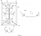
- FIG 14 shows yet another embodiment.
- This sensor according to the invention comprises a groove in the shape of an elongated inverted pyramid, having a rib at the top instead of a tip.
- Slanted resistive paths are provided on the sidewalls and along the slanted ribs of the pyramid, in the same manner and numbered with the same numerical references as for the embodiment of Figure 7 .
- planar resistive paths 15-18 are provided in the vicinity of the cavity.
- an area 70 comprising the elongated upper rib of the pyramid is subjected to silicidation, so that this area represents an essentially zero resistance. This allows to maintain all the formulas as described above for the pyramid with a tip.
- contacts could be provided in the middle (i.e. the common area of resistive paths 2 and 3) and at the outer ends (common areas of resistive paths 29,5,27 and 26,4,28) of the elongated upper rib.
- the inverted elongated pyramid-shaped cavity of Figure 14 is once again equivalently embodied by a positive elongated pyramid extending out from the substrate with resistive paths on the sidewalls and along the slanted ribs of the pyramid.
- a sensor of the invention may comprise multiple cavities or equivalent positive 3D shapes oriented at different angles in the xy plane and provided with slanted resistive paths and planar resistive paths as described above.
- multiple elongated grooves like the ones shown in Figures 13 and 14 may be provided with longitudinal axes oriented in the plane of the drawing at mutual angles different from 90°.
- the additional orientations may be required for deriving independent equations that allow to determine the normal stress components ⁇ xx , ⁇ yy and ⁇ zz in a temperature-compensated way.
- a second groove may be provided at 45° to the first.
- the orientation of the slanted resistive paths relative to the slanted sidewalls of the cavities, prisms or pyramids is not limited to the above-shown examples.
- the slanted resistive paths 2 to 5 need not necessarily run between the middle of the sides of the ground plane of the pyramid and the tip area 11.
- slanted resistive paths do not run from the edge of the cavity to the bottom, but only run along a portion of a slanted sidewall.
- the resistive paths can be produced by implanting portions of the substrate with dopant elements having one of two opposite polarity types, commonly referred to as p-type or n-type dopants.
- the coefficients of the piezo-resistive matrix used in the expression (1) are different for n-type and for p-type resistors.
- the slanted resistors R xz and R yz are preferably produced in p-type silicon because the ⁇ 44 coefficient is very small for an n-type resistor, leading to an inaccurate determination of ⁇ xz from equations (5) and (6).
- the set of equations (17)(18)(21) is preferably based on n-type resistors.
- the sensor of the invention may comprise two versions of any of the above-described designs, one with p-type resistors and one with n-type resistors. Alternatively, the sensor may comprise both polarity types in a single design.
- Figure 15 shows an example of the latter case for determining all the stress components.
- Planar p-type as well as n-type resistors are provided around a single cavity, preferably matched on opposite sides of the cavity.
- P-type resistive paths are indicated by ⁇ +' signs and n-type are indicated by '-' signs in the drawing.
- the slanted resistors on the side walls are p-type while the slanted resistors along the ribs of the pyramid are n-type.
Landscapes
- Physics & Mathematics (AREA)
- General Physics & Mathematics (AREA)
- Pressure Sensors (AREA)
Claims (14)
- Spannungssensor zum Überwachen und/oder Messen von Spannung in einer Halbleiterkomponente, wobei der Spannungssensor ein Substrat (50) umfasst,
das aus einem piezoresistiven Halbleitermaterial gebildet ist, wobei das Substrat eine planare Hauptoberfläche (100) umfasst, wobei der Sensor weiter Folgendes umfasst:- mindestens eine geneigte Oberfläche (111, 112) des Substratmaterials, wobei die geneigte Oberfläche durch einen schrägen Neigungswinkel in Bezug auf die Hauptoberfläche des Substrats definiert ist,- mindestens einen Widerstandspfad (R1, R2), der sich auf mindestens einem Teil der geneigten Oberfläche erstreckt, wobei der Widerstandspfad relativ zur geneigten Oberfläche gerade ist und dadurch einen geneigten Widerstandspfad in Bezug auf die Hauptoberfläche bildet,- eine Vielzahl von Kontakten (6, 7, 8, 9), die elektrisch mit dem mindestens einen geneigten Widerstandspfad verbunden sind, und Anschlüsse zum Zugreifen auf den geneigten Widerstandspfad, wodurch es möglich wird, den elektrischen Widerstand des Widerstandspfads zu messen und daraus eine Beurteilung der Scherspannung in einer Ebene abzuleiten, die nicht parallel zur Hauptoberfläche des Substrats ist,
dadurch gekennzeichnet, dass:- der Spannungssensor mindestens ein Paar der geneigten Oberflächen (111, 112) umfasst, die komplementäre Neigungswinkel relativ zur Hauptoberfläche (100) aufweisen, und mindestens ein Paar der Widerstandspfade (R1, R2) umfasst, die in einer ersten Ebene liegen, der erste Pfad auf der ersten geneigten Oberfläche und der zweite Pfad auf der zweiten geneigten Oberfläche, wobei das Paar geneigter Widerstandspfade auch komplementäre Neigungswinkel relativ zur Hauptoberfläche (100) aufweist und wobei der Sensor konfiguriert ist, um die Scherspannung in der ersten Ebene zu messen, die durch das Paar von Widerstandspfaden definiert ist. - Spannungssensor nach Anspruch 1, der zwei der Paare geneigter Oberflächen und geneigter Widerstandspfade (2, 3; 4, 5) umfasst und konfiguriert ist, um die Scherspannung in einer ersten und zweiten Ebene zu messen, wobei die Ebenen zwei zueinander nicht parallele Ebenen sind.
- Spannungssensor nach einem der vorstehenden Ansprüche, der weiter eine Vielzahl von planaren Widerstandspfaden (15-18) umfasst, die parallel zur Ebene der Hauptoberfläche (100) des Substrats (50) verlaufen und in der Nähe der geneigten Widerstandspfade angeordnet sind, sowie eine Vielzahl von Kontakten (20-23) und Anschlüssen zum Zugreifen auf die planaren Widerstandspfade, wodurch es möglich wird, den elektrischen Widerstand der planaren Pfade zu messen und daraus eine Bewertung einer oder mehrerer zusätzlicher Spannungskomponenten abzuleiten.
- Spannungssensor nach einem der vorstehenden Ansprüche, wobei die eine oder die mehreren geneigten Oberflächen die geneigten Seitenwände eines oder mehrerer Hohlräume (1, 101, 110) sind, die zur Hauptoberfläche (100) des Substrats oder zu einer anderen Oberfläche (122) des Substrats hin offen sind und/oder wobei die geneigten Oberflächen die geneigten Seitenwände dreidimensionaler Formen (1', 101') sind, die sich von der Hauptoberfläche (100) des Substrats oder von einer anderen Oberfläche (122) des Substrats nach außen erstrecken.
- Spannungssensor nach Anspruch 4, umfassend:- einen Hohlraum (1) oder eine 3D-Form (1'), die die Form einer vierwandigen Pyramide oder eines Kegelstumpfs einer vierwandigen Pyramide aufweisen, umfassend eine rechteckige oder quadratische Basis, einen mittig angeordneten Spitzenbereich (11), vier geneigte Wände, die sich jeweils zwischen den vier Kanten der Basis und dem Spitzenbereich erstrecken, wobei die vier Wände zwei Paare geneigter Oberflächen bilden, wobei die Oberflächen jedes Paares komplementäre Neigungswinkel relativ zur Hauptoberfläche (100) des Substrats aufweisen, und vier geneigte Rippen, die sich jeweils zwischen den Ecken der Basis und dem Spitzenbereich erstrecken,- vier elektrische Kontakte (6, 7, 8, 9),- vier geneigte Widerstandspfade jeweils auf den vier geneigten Oberflächen, wobei sich die vier Pfade zwischen dem Spitzenbereich (11) und den vier elektrischen Kontakten erstrecken, wobei die Pfade auf gegenüberliegenden Oberflächen komplementäre Neigungswinkel relativ zur Hauptoberfläche (100) des Substrats aufweisen.
- Spannungssensor nach Anspruch 5, umfassend einen fünften elektrischen Kontakt (10), der sich im Spitzenbereich (11) befindet, wobei sich die vier Widerstandspfade (2, 3, 4, 5) jeweils zwischen den vier Kontakten (6, 7, 8, 9) und dem fünften Kontakt (10) erstrecken.
- Spannungssensor nach Anspruch 5, wobei die vier geneigten Widerstandspfade im Spitzenbereich (11) zusammenlaufen und wobei die geneigten Widerstandspfade an gegenüberliegenden Wänden des Hohlraums oder der 3D-Form hinsichtlich ihres elektrischen Widerstands aufeinander abgestimmt sind, d. h. die Widerstände der Widerstandspfade sind bei einem Referenzzustand gleich, der so gewählt ist, dass er einem theoretischen Nullspannungszustand möglichst nahe kommt.
- Spannungssensor nach einem der Ansprüche 5 bis 7, weiter umfassend:- zwei planare Widerstandspfade (15, 17) in der Nähe des Hohlraums oder der 3D-Form (1,1'), wobei die zwei planaren Pfade entlang senkrechter Linien in der Ebene der Hauptoberfläche des Substrats verlaufen,- elektrische Kontakte (23, 22, 20) am Anfangs- und Endpunkt jedes planaren Widerstandspfads und Anschlüsse zum Zugreifen auf die Kontakte,- vier zusätzliche elektrische Kontakte (30, 31, 32, 33), die um den Hohlraum oder die 3D-Form herum platziert sind, einer an jeder der vier Ecken des Hohlraums oder der 3D-Form, und Anschlüsse zum Zugreifen auf die Eckkontakte,- vier geneigte Widerstandspfade (26, 27, 28, 29), wobei jeder Pfad entlang einer der Rippen des Hohlraums oder der 3D-Form zwischen den jeweiligen Eckkontakten und dem Spitzenbereich (11) des Hohlraums oder der 3D-Form verläuft.
- Spannungssensor nach Anspruch 8, der zwei zusätzliche planare Widerstandspfade (16, 18) sowie Kontakte (20, 21, 22) am Anfangs- und Endpunkt jedes zusätzlichen planaren Pfads umfasst, wobei:- die zwei zusätzlichen ebenen Pfade (16, 18) jeweils parallel zu den zwei senkrechten ebenen Pfaden (15, 17) verlaufen,- die zwei zusätzlichen planaren Pfade auf der gegenüberliegenden Seite des Hohlraums (1) oder der 3D-Form (1') in Bezug auf die jeweiligen senkrechten planaren Pfade verlaufen,- jedes Paar paralleler planarer Widerstandspfade hinsichtlich seines elektrischen Widerstands aufeinander abgestimmt ist.
- Spannungssensor nach Anspruch 9, wobei die zwei Paare paralleler Widerstandspfade die Seitenkanten eines Rechtecks bilden, wobei vier Kontakte an den Ecken des Rechtecks platziert sind.
- Spannungssensor nach einem der Ansprüche 8 bis 10, weiter umfassend:- zwei planare Widerstandspfade (15, 17) in der Nähe des Hohlraums oder der 3D-Form, wobei die zwei planaren Pfade entlang senkrechter Linien in der Ebene der Hauptoberfläche des Substrats verlaufen,- Kontakte (23, 22, 20) am Anfangs- und Endpunkt jedes planaren Widerstandspfads und Anschlüsse zum Zugreifen auf die Kontakte,- einen zweiten Hohlraum (25) oder eine 3D-Form derselben Form wie der erste Hohlraum oder die 3D-Form (1, 1') und in unmittelbarer Nähe zum ersten Hohlraum (1) oder zur 3D-Form platziert,- vier Kontakte (30, 31, 32, 33), die um den zweiten Hohlraum oder die 3D-Form herum an den vier Ecken des zweiten Hohlraums oder der 3D-Form platziert sind, und Anschlüsse, die Zugreifen auf die Eckkontakte ermöglichen,- vier geneigte Widerstandspfade (26, 27, 28, 29), wobei jeder Pfad entlang der Rippen des zweiten Hohlraums oder der 3D-Form zwischen den jeweiligen Eckkontakten und dem Spitzenbereich des zweiten Hohlraums oder der 3D-Form verläuft.
- Spannungssensor nach einem der vorstehenden Ansprüche, wobei das Substratmaterial ein kristallines Halbleitermaterial ist und wobei die Neigungswinkel durch die kristallographische Struktur des Materials definiert sind.
- Spannungssensor nach einem der vorstehenden Ansprüche, umfassend mehrere Widerstandspfade, die durch Implantation von Dotierstoffelementen in schmalen Bereichen der geneigten Oberflächen und gegebenenfalls in schmalen Bereichen der Hauptoberfläche des Substrats oder einer dazu parallelen Oberfläche erhalten werden und wobei der Sensor Widerstandspfade, die durch Implantation von Dotierstoffelementen eines ersten Polaritätstyps gebildet werden, sowie Widerstandspfade, die durch Implantation von Dotierstoffelementen eines zweiten Polaritätstyps gebildet werden, der dem ersten entgegengesetzt ist, umfasst.
- Halbleiterkomponente, die einen Spannungssensor nach einem der vorstehenden Ansprüche umfasst.
Priority Applications (3)
| Application Number | Priority Date | Filing Date | Title |
|---|---|---|---|
| EP17189517.0A EP3450947B1 (de) | 2017-09-05 | 2017-09-05 | Spannungssensor für halbleiterbauelemente |
| JP2018149619A JP7174562B2 (ja) | 2017-09-05 | 2018-08-08 | 半導体部品用の応力センサ |
| US16/121,369 US10607901B2 (en) | 2017-09-05 | 2018-09-04 | Stress sensor for semiconductor components |
Applications Claiming Priority (1)
| Application Number | Priority Date | Filing Date | Title |
|---|---|---|---|
| EP17189517.0A EP3450947B1 (de) | 2017-09-05 | 2017-09-05 | Spannungssensor für halbleiterbauelemente |
Publications (2)
| Publication Number | Publication Date |
|---|---|
| EP3450947A1 EP3450947A1 (de) | 2019-03-06 |
| EP3450947B1 true EP3450947B1 (de) | 2024-01-17 |
Family
ID=59829194
Family Applications (1)
| Application Number | Title | Priority Date | Filing Date |
|---|---|---|---|
| EP17189517.0A Active EP3450947B1 (de) | 2017-09-05 | 2017-09-05 | Spannungssensor für halbleiterbauelemente |
Country Status (3)
| Country | Link |
|---|---|
| US (1) | US10607901B2 (de) |
| EP (1) | EP3450947B1 (de) |
| JP (1) | JP7174562B2 (de) |
Families Citing this family (10)
| Publication number | Priority date | Publication date | Assignee | Title |
|---|---|---|---|---|
| CN109983326A (zh) * | 2016-11-09 | 2019-07-05 | Imec 非营利协会 | 用于组合的stem和eds断层摄影的装备 |
| IT201700044301A1 (it) * | 2017-04-21 | 2018-10-21 | St Microelectronics Srl | Sensore di sforzo per il monitoraggio dello stato di salute di strutture fabbricate quali costruzioni, edifici, infrastrutture e simili |
| JP7133763B2 (ja) * | 2019-05-09 | 2022-09-09 | 株式会社テック技販 | 荷重センサー、および、荷重検出方法 |
| US11650110B2 (en) * | 2020-11-04 | 2023-05-16 | Honeywell International Inc. | Rosette piezo-resistive gauge circuit for thermally compensated measurement of full stress tensor |
| JP7809927B2 (ja) * | 2021-08-04 | 2026-02-03 | 株式会社大林組 | 計測装置及び、計測方法 |
| US12259285B2 (en) | 2021-08-13 | 2025-03-25 | Analog Devices, Inc. | Package stress sensor |
| US12523551B2 (en) | 2021-08-13 | 2026-01-13 | Analog Devices, Inc. | Package stress sensor with hall cancellation |
| CN114112129B (zh) * | 2021-11-19 | 2022-08-05 | 苏州纳芯微电子股份有限公司 | 一种基板应力传感器及传感设备 |
| US20260043697A1 (en) * | 2024-08-12 | 2026-02-12 | Texas Instruments Incorporated | Integrated circuit stress sensor |
| CN119901397B (zh) * | 2025-03-27 | 2025-06-20 | 中国空气动力研究与发展中心超高速空气动力研究所 | 圆锥模型表面摩阻测量的共型mems摩阻传感器及组装方法 |
Family Cites Families (18)
| Publication number | Priority date | Publication date | Assignee | Title |
|---|---|---|---|---|
| JPS5664472A (en) * | 1979-10-30 | 1981-06-01 | Nec Corp | Detector for strain by semiconductor |
| JPS60154574A (ja) * | 1984-01-23 | 1985-08-14 | Fuji Electric Corp Res & Dev Ltd | 圧覚センサ |
| JPS6389282A (ja) * | 1986-09-30 | 1988-04-20 | 株式会社東芝 | 触覚センサ |
| JPH06130083A (ja) * | 1992-04-01 | 1994-05-13 | Nec Corp | 半導体加速度センサ |
| JP3237256B2 (ja) * | 1993-01-12 | 2001-12-10 | 株式会社デンソー | 加速度検出回路 |
| US6150681A (en) | 1998-07-24 | 2000-11-21 | Silicon Microstructures, Inc. | Monolithic flow sensor and pressure sensor |
| JP3368344B2 (ja) | 1998-11-24 | 2003-01-20 | 学校法人立命館 | 半導体ひずみゲージ及びそれを用いたひずみ測定方法 |
| US6951143B1 (en) * | 2000-11-28 | 2005-10-04 | Michelin Recherche Et Technique S.A. | Three-axis sensor assembly for use in an elastomeric material |
| DE10231727A1 (de) | 2002-07-13 | 2004-01-22 | Robert Bosch Gmbh | Mikromechanische Drucksensorvorrichtung und entsprechende Messanordnung |
| JP2004340858A (ja) | 2003-05-19 | 2004-12-02 | Sharp Corp | 物理量センサーおよびその製造方法 |
| US7765880B2 (en) * | 2008-05-19 | 2010-08-03 | Hong Kong Polytechnic University | Flexible piezoresistive interfacial shear and normal force sensor and sensor array |
| FR2950427B1 (fr) * | 2009-09-21 | 2012-10-12 | Ct Tech Des Ind Mecaniques | Jauge de deformation en circuit integre autoalimentee |
| CA2806543C (en) | 2010-11-24 | 2016-05-17 | The Governors Of The University Of Alberta | A novel embedded 3d stress and temperature sensor utilizing silicon doping manipulation |
| KR102081892B1 (ko) * | 2013-09-05 | 2020-02-26 | 삼성전자주식회사 | 압저항(piezo-resistive) 전극을 구비한 저항성 압력 센서 |
| CN104819789B (zh) | 2015-02-10 | 2017-05-24 | 华进半导体封装先导技术研发中心有限公司 | 一种应力传感器及制作方法 |
| WO2018067396A1 (en) * | 2016-10-03 | 2018-04-12 | Flir Systems, Inc. | Methods for routing electrical interconnections and resultant structures |
| US10804115B2 (en) * | 2017-08-03 | 2020-10-13 | General Electric Company | Electronics package with integrated interconnect structure and method of manufacturing thereof |
| TWI695965B (zh) * | 2017-12-21 | 2020-06-11 | 愛盛科技股份有限公司 | 磁場感測裝置 |
-
2017
- 2017-09-05 EP EP17189517.0A patent/EP3450947B1/de active Active
-
2018
- 2018-08-08 JP JP2018149619A patent/JP7174562B2/ja active Active
- 2018-09-04 US US16/121,369 patent/US10607901B2/en active Active
Also Published As
| Publication number | Publication date |
|---|---|
| JP2019060855A (ja) | 2019-04-18 |
| EP3450947A1 (de) | 2019-03-06 |
| US10607901B2 (en) | 2020-03-31 |
| US20190074231A1 (en) | 2019-03-07 |
| JP7174562B2 (ja) | 2022-11-17 |
Similar Documents
| Publication | Publication Date | Title |
|---|---|---|
| EP3450947B1 (de) | Spannungssensor für halbleiterbauelemente | |
| US10775248B2 (en) | MEMS strain gauge sensor and manufacturing method | |
| US11255740B2 (en) | Pressure gauge chip and manufacturing process thereof | |
| Kumar et al. | Design principles and considerations for the ‘ideal’silicon piezoresistive pressure sensor: a focused review | |
| US10768064B2 (en) | MEMS pressure gauge sensor and manufacturing method | |
| US20150142342A1 (en) | Method and Device for Sensing Isotropic Stress and Providing a Compensation for the Piezo-Hall Effect | |
| US20190145842A1 (en) | A dual-cavity pressure sensor die and the method of making same | |
| CN110389237B (zh) | 一种面内双轴加速度传感器芯片及其制备方法 | |
| EP0195232B1 (de) | Piezoresistiver Belastungsfühler | |
| JP2575939B2 (ja) | 半導体加速度センサ | |
| US9857258B2 (en) | Pressure sensor to sense multi-directional movement | |
| CN111521304B (zh) | 一种微压传感器芯片及其制备方法 | |
| JP4335545B2 (ja) | 圧力と加速度との双方を検出するセンサおよびその製造方法 | |
| KR20030068437A (ko) | 가속도 센서 | |
| US20130205910A1 (en) | Novel embedded 3d stress and temperature sensor utilizing silicon doping manipulation | |
| JP4431475B2 (ja) | 半導体型3軸加速度センサ | |
| US8511170B2 (en) | Pressure transducer having structure for monitoring surface charge | |
| US6865951B2 (en) | Semiconductor pressure sensor | |
| KR101196064B1 (ko) | 압력 센서 및 압력 센서의 제조 방법 | |
| Gharib et al. | On the feasibility of a new approach for developing a piezoresistive 3D stress sensing rosette | |
| EP3056865B1 (de) | Sensorenanordnung | |
| EP3323778B1 (de) | Mems-vorrichtung und verfahren zur kalibrierung einer mems-vorrichtung | |
| JP2011027611A (ja) | 半導体圧力センサ及びその製造方法 | |
| CN118882901B (zh) | 六轴力传感器及其制造方法 | |
| RU2507490C1 (ru) | Датчик абсолютного давления повышенной точности на основе полупроводникового чувствительного элемента с жестким центром |
Legal Events
| Date | Code | Title | Description |
|---|---|---|---|
| PUAI | Public reference made under article 153(3) epc to a published international application that has entered the european phase |
Free format text: ORIGINAL CODE: 0009012 |
|
| STAA | Information on the status of an ep patent application or granted ep patent |
Free format text: STATUS: THE APPLICATION HAS BEEN PUBLISHED |
|
| AK | Designated contracting states |
Kind code of ref document: A1 Designated state(s): AL AT BE BG CH CY CZ DE DK EE ES FI FR GB GR HR HU IE IS IT LI LT LU LV MC MK MT NL NO PL PT RO RS SE SI SK SM TR |
|
| AX | Request for extension of the european patent |
Extension state: BA ME |
|
| STAA | Information on the status of an ep patent application or granted ep patent |
Free format text: STATUS: REQUEST FOR EXAMINATION WAS MADE |
|
| 17P | Request for examination filed |
Effective date: 20190905 |
|
| RBV | Designated contracting states (corrected) |
Designated state(s): AL AT BE BG CH CY CZ DE DK EE ES FI FR GB GR HR HU IE IS IT LI LT LU LV MC MK MT NL NO PL PT RO RS SE SI SK SM TR |
|
| STAA | Information on the status of an ep patent application or granted ep patent |
Free format text: STATUS: EXAMINATION IS IN PROGRESS |
|
| 17Q | First examination report despatched |
Effective date: 20211028 |
|
| REG | Reference to a national code |
Ref country code: DE Ref legal event code: R079 Free format text: PREVIOUS MAIN CLASS: G01L0001160000 Ref country code: DE Ref legal event code: R079 Ref document number: 602017078486 Country of ref document: DE Free format text: PREVIOUS MAIN CLASS: G01L0001160000 Ipc: G01L0005162000 |
|
| GRAP | Despatch of communication of intention to grant a patent |
Free format text: ORIGINAL CODE: EPIDOSNIGR1 |
|
| STAA | Information on the status of an ep patent application or granted ep patent |
Free format text: STATUS: GRANT OF PATENT IS INTENDED |
|
| RIC1 | Information provided on ipc code assigned before grant |
Ipc: G01L 1/18 20060101ALI20230821BHEP Ipc: G01L 1/16 20060101ALI20230821BHEP Ipc: G01L 1/22 20060101ALI20230821BHEP Ipc: G01L 5/162 20200101AFI20230821BHEP |
|
| INTG | Intention to grant announced |
Effective date: 20230912 |
|
| RIN1 | Information on inventor provided before grant (corrected) |
Inventor name: VAN HUYLENBROECK, STEFAAN Inventor name: VAN DER PLAS, MR. GEERT Inventor name: HIBLOT, GASPARD |
|
| P01 | Opt-out of the competence of the unified patent court (upc) registered |
Effective date: 20231031 |
|
| GRAS | Grant fee paid |
Free format text: ORIGINAL CODE: EPIDOSNIGR3 |
|
| GRAA | (expected) grant |
Free format text: ORIGINAL CODE: 0009210 |
|
| STAA | Information on the status of an ep patent application or granted ep patent |
Free format text: STATUS: THE PATENT HAS BEEN GRANTED |
|
| AK | Designated contracting states |
Kind code of ref document: B1 Designated state(s): AL AT BE BG CH CY CZ DE DK EE ES FI FR GB GR HR HU IE IS IT LI LT LU LV MC MK MT NL NO PL PT RO RS SE SI SK SM TR |
|
| REG | Reference to a national code |
Ref country code: GB Ref legal event code: FG4D |
|
| REG | Reference to a national code |
Ref country code: CH Ref legal event code: EP |
|
| REG | Reference to a national code |
Ref country code: DE Ref legal event code: R096 Ref document number: 602017078486 Country of ref document: DE |
|
| REG | Reference to a national code |
Ref country code: IE Ref legal event code: FG4D |
|
| REG | Reference to a national code |
Ref country code: LT Ref legal event code: MG9D |
|
| REG | Reference to a national code |
Ref country code: NL Ref legal event code: MP Effective date: 20240117 |
|
| REG | Reference to a national code |
Ref country code: AT Ref legal event code: MK05 Ref document number: 1650832 Country of ref document: AT Kind code of ref document: T Effective date: 20240117 |
|
| PG25 | Lapsed in a contracting state [announced via postgrant information from national office to epo] |
Ref country code: NL Free format text: LAPSE BECAUSE OF FAILURE TO SUBMIT A TRANSLATION OF THE DESCRIPTION OR TO PAY THE FEE WITHIN THE PRESCRIBED TIME-LIMIT Effective date: 20240117 |
|
| PG25 | Lapsed in a contracting state [announced via postgrant information from national office to epo] |
Ref country code: NL Free format text: LAPSE BECAUSE OF FAILURE TO SUBMIT A TRANSLATION OF THE DESCRIPTION OR TO PAY THE FEE WITHIN THE PRESCRIBED TIME-LIMIT Effective date: 20240117 |
|
| PG25 | Lapsed in a contracting state [announced via postgrant information from national office to epo] |
Ref country code: IS Free format text: LAPSE BECAUSE OF FAILURE TO SUBMIT A TRANSLATION OF THE DESCRIPTION OR TO PAY THE FEE WITHIN THE PRESCRIBED TIME-LIMIT Effective date: 20240517 |
|
| PG25 | Lapsed in a contracting state [announced via postgrant information from national office to epo] |
Ref country code: LT Free format text: LAPSE BECAUSE OF FAILURE TO SUBMIT A TRANSLATION OF THE DESCRIPTION OR TO PAY THE FEE WITHIN THE PRESCRIBED TIME-LIMIT Effective date: 20240117 |
|
| PG25 | Lapsed in a contracting state [announced via postgrant information from national office to epo] |
Ref country code: GR Free format text: LAPSE BECAUSE OF FAILURE TO SUBMIT A TRANSLATION OF THE DESCRIPTION OR TO PAY THE FEE WITHIN THE PRESCRIBED TIME-LIMIT Effective date: 20240418 |
|
| PG25 | Lapsed in a contracting state [announced via postgrant information from national office to epo] |
Ref country code: RS Free format text: LAPSE BECAUSE OF FAILURE TO SUBMIT A TRANSLATION OF THE DESCRIPTION OR TO PAY THE FEE WITHIN THE PRESCRIBED TIME-LIMIT Effective date: 20240417 Ref country code: HR Free format text: LAPSE BECAUSE OF FAILURE TO SUBMIT A TRANSLATION OF THE DESCRIPTION OR TO PAY THE FEE WITHIN THE PRESCRIBED TIME-LIMIT Effective date: 20240117 |
|
| PG25 | Lapsed in a contracting state [announced via postgrant information from national office to epo] |
Ref country code: ES Free format text: LAPSE BECAUSE OF FAILURE TO SUBMIT A TRANSLATION OF THE DESCRIPTION OR TO PAY THE FEE WITHIN THE PRESCRIBED TIME-LIMIT Effective date: 20240117 |
|
| PG25 | Lapsed in a contracting state [announced via postgrant information from national office to epo] |
Ref country code: AT Free format text: LAPSE BECAUSE OF FAILURE TO SUBMIT A TRANSLATION OF THE DESCRIPTION OR TO PAY THE FEE WITHIN THE PRESCRIBED TIME-LIMIT Effective date: 20240117 |
|
| PG25 | Lapsed in a contracting state [announced via postgrant information from national office to epo] |
Ref country code: RS Free format text: LAPSE BECAUSE OF FAILURE TO SUBMIT A TRANSLATION OF THE DESCRIPTION OR TO PAY THE FEE WITHIN THE PRESCRIBED TIME-LIMIT Effective date: 20240417 Ref country code: NO Free format text: LAPSE BECAUSE OF FAILURE TO SUBMIT A TRANSLATION OF THE DESCRIPTION OR TO PAY THE FEE WITHIN THE PRESCRIBED TIME-LIMIT Effective date: 20240417 Ref country code: LT Free format text: LAPSE BECAUSE OF FAILURE TO SUBMIT A TRANSLATION OF THE DESCRIPTION OR TO PAY THE FEE WITHIN THE PRESCRIBED TIME-LIMIT Effective date: 20240117 Ref country code: IS Free format text: LAPSE BECAUSE OF FAILURE TO SUBMIT A TRANSLATION OF THE DESCRIPTION OR TO PAY THE FEE WITHIN THE PRESCRIBED TIME-LIMIT Effective date: 20240517 Ref country code: HR Free format text: LAPSE BECAUSE OF FAILURE TO SUBMIT A TRANSLATION OF THE DESCRIPTION OR TO PAY THE FEE WITHIN THE PRESCRIBED TIME-LIMIT Effective date: 20240117 Ref country code: GR Free format text: LAPSE BECAUSE OF FAILURE TO SUBMIT A TRANSLATION OF THE DESCRIPTION OR TO PAY THE FEE WITHIN THE PRESCRIBED TIME-LIMIT Effective date: 20240418 Ref country code: FI Free format text: LAPSE BECAUSE OF FAILURE TO SUBMIT A TRANSLATION OF THE DESCRIPTION OR TO PAY THE FEE WITHIN THE PRESCRIBED TIME-LIMIT Effective date: 20240117 Ref country code: ES Free format text: LAPSE BECAUSE OF FAILURE TO SUBMIT A TRANSLATION OF THE DESCRIPTION OR TO PAY THE FEE WITHIN THE PRESCRIBED TIME-LIMIT Effective date: 20240117 Ref country code: BG Free format text: LAPSE BECAUSE OF FAILURE TO SUBMIT A TRANSLATION OF THE DESCRIPTION OR TO PAY THE FEE WITHIN THE PRESCRIBED TIME-LIMIT Effective date: 20240117 Ref country code: AT Free format text: LAPSE BECAUSE OF FAILURE TO SUBMIT A TRANSLATION OF THE DESCRIPTION OR TO PAY THE FEE WITHIN THE PRESCRIBED TIME-LIMIT Effective date: 20240117 |
|
| PG25 | Lapsed in a contracting state [announced via postgrant information from national office to epo] |
Ref country code: PL Free format text: LAPSE BECAUSE OF FAILURE TO SUBMIT A TRANSLATION OF THE DESCRIPTION OR TO PAY THE FEE WITHIN THE PRESCRIBED TIME-LIMIT Effective date: 20240117 Ref country code: PT Free format text: LAPSE BECAUSE OF FAILURE TO SUBMIT A TRANSLATION OF THE DESCRIPTION OR TO PAY THE FEE WITHIN THE PRESCRIBED TIME-LIMIT Effective date: 20240517 |
|
| PG25 | Lapsed in a contracting state [announced via postgrant information from national office to epo] |
Ref country code: SE Free format text: LAPSE BECAUSE OF FAILURE TO SUBMIT A TRANSLATION OF THE DESCRIPTION OR TO PAY THE FEE WITHIN THE PRESCRIBED TIME-LIMIT Effective date: 20240117 Ref country code: PT Free format text: LAPSE BECAUSE OF FAILURE TO SUBMIT A TRANSLATION OF THE DESCRIPTION OR TO PAY THE FEE WITHIN THE PRESCRIBED TIME-LIMIT Effective date: 20240517 Ref country code: PL Free format text: LAPSE BECAUSE OF FAILURE TO SUBMIT A TRANSLATION OF THE DESCRIPTION OR TO PAY THE FEE WITHIN THE PRESCRIBED TIME-LIMIT Effective date: 20240117 Ref country code: LV Free format text: LAPSE BECAUSE OF FAILURE TO SUBMIT A TRANSLATION OF THE DESCRIPTION OR TO PAY THE FEE WITHIN THE PRESCRIBED TIME-LIMIT Effective date: 20240117 |
|
| PG25 | Lapsed in a contracting state [announced via postgrant information from national office to epo] |
Ref country code: DK Free format text: LAPSE BECAUSE OF FAILURE TO SUBMIT A TRANSLATION OF THE DESCRIPTION OR TO PAY THE FEE WITHIN THE PRESCRIBED TIME-LIMIT Effective date: 20240117 |
|
| PG25 | Lapsed in a contracting state [announced via postgrant information from national office to epo] |
Ref country code: SM Free format text: LAPSE BECAUSE OF FAILURE TO SUBMIT A TRANSLATION OF THE DESCRIPTION OR TO PAY THE FEE WITHIN THE PRESCRIBED TIME-LIMIT Effective date: 20240117 |
|
| REG | Reference to a national code |
Ref country code: DE Ref legal event code: R097 Ref document number: 602017078486 Country of ref document: DE |
|
| PG25 | Lapsed in a contracting state [announced via postgrant information from national office to epo] |
Ref country code: EE Free format text: LAPSE BECAUSE OF FAILURE TO SUBMIT A TRANSLATION OF THE DESCRIPTION OR TO PAY THE FEE WITHIN THE PRESCRIBED TIME-LIMIT Effective date: 20240117 Ref country code: CZ Free format text: LAPSE BECAUSE OF FAILURE TO SUBMIT A TRANSLATION OF THE DESCRIPTION OR TO PAY THE FEE WITHIN THE PRESCRIBED TIME-LIMIT Effective date: 20240117 |
|
| PG25 | Lapsed in a contracting state [announced via postgrant information from national office to epo] |
Ref country code: SK Free format text: LAPSE BECAUSE OF FAILURE TO SUBMIT A TRANSLATION OF THE DESCRIPTION OR TO PAY THE FEE WITHIN THE PRESCRIBED TIME-LIMIT Effective date: 20240117 |
|
| PG25 | Lapsed in a contracting state [announced via postgrant information from national office to epo] |
Ref country code: SM Free format text: LAPSE BECAUSE OF FAILURE TO SUBMIT A TRANSLATION OF THE DESCRIPTION OR TO PAY THE FEE WITHIN THE PRESCRIBED TIME-LIMIT Effective date: 20240117 Ref country code: SK Free format text: LAPSE BECAUSE OF FAILURE TO SUBMIT A TRANSLATION OF THE DESCRIPTION OR TO PAY THE FEE WITHIN THE PRESCRIBED TIME-LIMIT Effective date: 20240117 Ref country code: RO Free format text: LAPSE BECAUSE OF FAILURE TO SUBMIT A TRANSLATION OF THE DESCRIPTION OR TO PAY THE FEE WITHIN THE PRESCRIBED TIME-LIMIT Effective date: 20240117 Ref country code: EE Free format text: LAPSE BECAUSE OF FAILURE TO SUBMIT A TRANSLATION OF THE DESCRIPTION OR TO PAY THE FEE WITHIN THE PRESCRIBED TIME-LIMIT Effective date: 20240117 Ref country code: DK Free format text: LAPSE BECAUSE OF FAILURE TO SUBMIT A TRANSLATION OF THE DESCRIPTION OR TO PAY THE FEE WITHIN THE PRESCRIBED TIME-LIMIT Effective date: 20240117 Ref country code: CZ Free format text: LAPSE BECAUSE OF FAILURE TO SUBMIT A TRANSLATION OF THE DESCRIPTION OR TO PAY THE FEE WITHIN THE PRESCRIBED TIME-LIMIT Effective date: 20240117 |
|
| PLBE | No opposition filed within time limit |
Free format text: ORIGINAL CODE: 0009261 |
|
| STAA | Information on the status of an ep patent application or granted ep patent |
Free format text: STATUS: NO OPPOSITION FILED WITHIN TIME LIMIT |
|
| PG25 | Lapsed in a contracting state [announced via postgrant information from national office to epo] |
Ref country code: IT Free format text: LAPSE BECAUSE OF FAILURE TO SUBMIT A TRANSLATION OF THE DESCRIPTION OR TO PAY THE FEE WITHIN THE PRESCRIBED TIME-LIMIT Effective date: 20240117 |
|
| 26N | No opposition filed |
Effective date: 20241018 |
|
| PG25 | Lapsed in a contracting state [announced via postgrant information from national office to epo] |
Ref country code: IT Free format text: LAPSE BECAUSE OF FAILURE TO SUBMIT A TRANSLATION OF THE DESCRIPTION OR TO PAY THE FEE WITHIN THE PRESCRIBED TIME-LIMIT Effective date: 20240117 |
|
| PG25 | Lapsed in a contracting state [announced via postgrant information from national office to epo] |
Ref country code: SI Free format text: LAPSE BECAUSE OF FAILURE TO SUBMIT A TRANSLATION OF THE DESCRIPTION OR TO PAY THE FEE WITHIN THE PRESCRIBED TIME-LIMIT Effective date: 20240117 Ref country code: MC Free format text: LAPSE BECAUSE OF FAILURE TO SUBMIT A TRANSLATION OF THE DESCRIPTION OR TO PAY THE FEE WITHIN THE PRESCRIBED TIME-LIMIT Effective date: 20240117 |
|
| REG | Reference to a national code |
Ref country code: CH Ref legal event code: PL |
|
| PG25 | Lapsed in a contracting state [announced via postgrant information from national office to epo] |
Ref country code: LU Free format text: LAPSE BECAUSE OF NON-PAYMENT OF DUE FEES Effective date: 20240905 |
|
| GBPC | Gb: european patent ceased through non-payment of renewal fee |
Effective date: 20240905 |
|
| PG25 | Lapsed in a contracting state [announced via postgrant information from national office to epo] |
Ref country code: GB Free format text: LAPSE BECAUSE OF NON-PAYMENT OF DUE FEES Effective date: 20240905 |
|
| REG | Reference to a national code |
Ref country code: BE Ref legal event code: MM Effective date: 20240930 |
|
| PG25 | Lapsed in a contracting state [announced via postgrant information from national office to epo] |
Ref country code: BE Free format text: LAPSE BECAUSE OF NON-PAYMENT OF DUE FEES Effective date: 20240930 |
|
| PG25 | Lapsed in a contracting state [announced via postgrant information from national office to epo] |
Ref country code: FR Free format text: LAPSE BECAUSE OF NON-PAYMENT OF DUE FEES Effective date: 20240930 |
|
| PG25 | Lapsed in a contracting state [announced via postgrant information from national office to epo] |
Ref country code: CH Free format text: LAPSE BECAUSE OF NON-PAYMENT OF DUE FEES Effective date: 20240930 |
|
| PG25 | Lapsed in a contracting state [announced via postgrant information from national office to epo] |
Ref country code: IE Free format text: LAPSE BECAUSE OF NON-PAYMENT OF DUE FEES Effective date: 20240905 |
|
| PGFP | Annual fee paid to national office [announced via postgrant information from national office to epo] |
Ref country code: DE Payment date: 20250820 Year of fee payment: 9 |
|
| PG25 | Lapsed in a contracting state [announced via postgrant information from national office to epo] |
Ref country code: CY Free format text: LAPSE BECAUSE OF FAILURE TO SUBMIT A TRANSLATION OF THE DESCRIPTION OR TO PAY THE FEE WITHIN THE PRESCRIBED TIME-LIMIT; INVALID AB INITIO Effective date: 20170905 |
|
| PG25 | Lapsed in a contracting state [announced via postgrant information from national office to epo] |
Ref country code: HU Free format text: LAPSE BECAUSE OF FAILURE TO SUBMIT A TRANSLATION OF THE DESCRIPTION OR TO PAY THE FEE WITHIN THE PRESCRIBED TIME-LIMIT; INVALID AB INITIO Effective date: 20170905 |