EP3465450B1 - Amélioration du débit dans des environnements openfabrics - Google Patents
Amélioration du débit dans des environnements openfabrics Download PDFInfo
- Publication number
- EP3465450B1 EP3465450B1 EP17733209.5A EP17733209A EP3465450B1 EP 3465450 B1 EP3465450 B1 EP 3465450B1 EP 17733209 A EP17733209 A EP 17733209A EP 3465450 B1 EP3465450 B1 EP 3465450B1
- Authority
- EP
- European Patent Office
- Prior art keywords
- header
- data
- buffers
- buffer
- rdma
- Prior art date
- Legal status (The legal status is an assumption and is not a legal conclusion. Google has not performed a legal analysis and makes no representation as to the accuracy of the status listed.)
- Active
Links
Images


Classifications
-
- H—ELECTRICITY
- H04—ELECTRIC COMMUNICATION TECHNIQUE
- H04L—TRANSMISSION OF DIGITAL INFORMATION, e.g. TELEGRAPHIC COMMUNICATION
- H04L67/00—Network arrangements or protocols for supporting network services or applications
- H04L67/01—Protocols
- H04L67/10—Protocols in which an application is distributed across nodes in the network
- H04L67/1097—Protocols in which an application is distributed across nodes in the network for distributed storage of data in networks, e.g. transport arrangements for network file system [NFS], storage area networks [SAN] or network attached storage [NAS]
-
- G—PHYSICS
- G06—COMPUTING OR CALCULATING; COUNTING
- G06F—ELECTRIC DIGITAL DATA PROCESSING
- G06F13/00—Interconnection of, or transfer of information or other signals between, memories, input/output devices or central processing units
- G06F13/14—Handling requests for interconnection or transfer
- G06F13/20—Handling requests for interconnection or transfer for access to input/output bus
- G06F13/28—Handling requests for interconnection or transfer for access to input/output bus using burst mode transfer, e.g. direct memory access DMA, cycle steal
-
- G—PHYSICS
- G06—COMPUTING OR CALCULATING; COUNTING
- G06F—ELECTRIC DIGITAL DATA PROCESSING
- G06F3/00—Input arrangements for transferring data to be processed into a form capable of being handled by the computer; Output arrangements for transferring data from processing unit to output unit, e.g. interface arrangements
- G06F3/06—Digital input from, or digital output to, record carriers, e.g. RAID, emulated record carriers or networked record carriers
- G06F3/0601—Interfaces specially adapted for storage systems
- G06F3/0602—Interfaces specially adapted for storage systems specifically adapted to achieve a particular effect
- G06F3/061—Improving I/O performance
-
- G—PHYSICS
- G06—COMPUTING OR CALCULATING; COUNTING
- G06F—ELECTRIC DIGITAL DATA PROCESSING
- G06F3/00—Input arrangements for transferring data to be processed into a form capable of being handled by the computer; Output arrangements for transferring data from processing unit to output unit, e.g. interface arrangements
- G06F3/06—Digital input from, or digital output to, record carriers, e.g. RAID, emulated record carriers or networked record carriers
- G06F3/0601—Interfaces specially adapted for storage systems
- G06F3/0628—Interfaces specially adapted for storage systems making use of a particular technique
- G06F3/0655—Vertical data movement, i.e. input-output transfer; data movement between one or more hosts and one or more storage devices
- G06F3/0659—Command handling arrangements, e.g. command buffers, queues, command scheduling
-
- G—PHYSICS
- G06—COMPUTING OR CALCULATING; COUNTING
- G06F—ELECTRIC DIGITAL DATA PROCESSING
- G06F3/00—Input arrangements for transferring data to be processed into a form capable of being handled by the computer; Output arrangements for transferring data from processing unit to output unit, e.g. interface arrangements
- G06F3/06—Digital input from, or digital output to, record carriers, e.g. RAID, emulated record carriers or networked record carriers
- G06F3/0601—Interfaces specially adapted for storage systems
- G06F3/0668—Interfaces specially adapted for storage systems adopting a particular infrastructure
- G06F3/067—Distributed or networked storage systems, e.g. storage area networks [SAN], network attached storage [NAS]
-
- H—ELECTRICITY
- H04—ELECTRIC COMMUNICATION TECHNIQUE
- H04L—TRANSMISSION OF DIGITAL INFORMATION, e.g. TELEGRAPHIC COMMUNICATION
- H04L67/00—Network arrangements or protocols for supporting network services or applications
- H04L67/50—Network services
- H04L67/56—Provisioning of proxy services
- H04L67/568—Storing data temporarily at an intermediate stage, e.g. caching
-
- G—PHYSICS
- G06—COMPUTING OR CALCULATING; COUNTING
- G06F—ELECTRIC DIGITAL DATA PROCESSING
- G06F2213/00—Indexing scheme relating to interconnection of, or transfer of information or other signals between, memories, input/output devices or central processing units
- G06F2213/28—DMA
- G06F2213/2806—Space or buffer allocation for DMA transfers
Definitions
- This disclosure relates to throughput.
- this disclosure relates to improving throughput in OpenFabrics computing environments.
- OFED TM OpenFabrics Enterprise Distribution
- RDMA Remote Direct Memory Access
- kernel bypass applications OFED
- OFED can be used in computing environments that require highly efficient networks, storage connectivity, and parallel computing.
- OFED provides kernel-level drivers, RDMA send/receive operations, services for parallel message passing (MPI), kernel bypasses of an operating system (OS), and kernel and user-level application programming interfaces (APIs). Therefore, OFED can be used for applications that require high efficiency computing, wire-speed messaging, microsecond latencies, and fast input/output (I/O) for storage and file systems.
- MPI parallel message passing
- OS operating system
- APIs kernel and user-level application programming interfaces
- RDMA involves direct memory access (DMA) from the memory of one computing system into that of another computing system without involving either computing system's OS.
- DMA direct memory access
- RDMA provides remote direct memory access, asynchronous work queues, and kernel bypass. RDMA permits increased throughput and low latency.
- OFED APIs can accept input parameters (e.g., in the form of a header and one or more data packets). Because the header is typically small in size (e.g., compared to the data), it is efficient to coalesce the data and the header to minimize the number of RDMA writes. However, coalescing the data and the header, while keeping the data page-boundary-aligned, can result in on-wire wastage (e.g., the amount of data that is sent or transferred over the network).
- on-wire wastage e.g., the amount of data that is sent or transferred over the network.
- US 2011/185032 A1 relates to a method for controlling a communication apparatus.
- US 2006/095611 A1 relates to a hardware supported peripheral component memory alignment method.
- US 2005/015549 A1 relates to a method for transferring data from a memory subsystem to a network adapter by extending data lengths to improve the memory subsystem and PCI bus efficiency.
- One such method involves receiving data and a header, and identifying buffers in which the data and the header are to be written. Placement information for the data and the header is determined based, at least in part, on a size of each buffer, a page-boundary-alignment of the data, and a header alignment of the header. The data and the header are then written to the buffer(s) using the placement information. In this example, data is written on page boundaries and the header is written on a header boundary.
- using the placement information results in the utilization of a minimum number of buffers and the data being page-boundary-aligned when written to the minimum number of buffers, as well as minimal (or zero) on-wire wastage.
- the placement information includes instructions to write the data and the header to a second to last buffer.
- the header and the data is coalesced (combined) into a Remote Direct Memory Access (RDMA) write by mapping the header and the data contained in multiple source buffers to one (or more) destination buffers based on the placement information.
- RDMA Remote Direct Memory Access
- the RDMA write which includes and is accompanied by a 32-bit data space containing metadata, is sent or transmitted to a destination along with the placement information.
- one or more additional buffers can be selected.
- the buffers include multiple destination buffers, and the minimum number of buffers include one or more destination buffers.
- data transfer between two (or more) computing systems can involve sending data and an accompanying header (as well as other metadata) directly from the memory of one computing system (e.g., from multiple source buffers) to the memory of another computing system (e.g., to one or more destination buffers.
- a header is typically small in size (e.g., 1k)
- performing a write operation solely to transfer the header from the memory of one computing system to the memory of another computing system is inefficient, not to mention resource intensive.
- coalesce or combine
- data and a header contained in multiple source buffers is mapped to a single destination buffer (or multiple destination buffers). This placement (or mapping) information is then transmitted from source buffers to one or more destination buffers along with the data and the header as part of a single write operation.
- OFED Open Fabrics Enterprise Distribution
- OFED OpenFabrics Software
- RDMA Remote Direct Memory Access
- OFED can be implemented in computing environments that require highly efficient networks, storage connectivity, and parallel computing.
- OFED provides kernel-level drivers, channel oriented RDMA and send/receive operations, kernel bypasses of an operating system (OS), and kernel and user-level application programming interfaces (APIs) (e.g., OFED API for RDMA transfer).
- OFED also provides services for parallel message passing (MPI), sockets data exchange (e.g., Session Description Protocol (SDP)), Network Attached Storage (NAS) and Storage Area Network (SAN) storage, and file systems.
- MPI parallel message passing
- SDP Session Description Protocol
- NAS Network Attached Storage
- SAN Storage Area Network
- RDMA involves direct memory access (DMA) from the memory of one computing system (e.g., a source computing system) into that of another computing system (e.g., a destination computing system) without involving either the source or destination computing system's OS.
- a network adapter of the source computing system can send a message to the network adapter of the destination computing system that permits the network adapter of the destination computing system to directly access data to (or from) the destination computing system's memory.
- a message in RDMA can include at least two types of messages.
- the first type is an RDMA write.
- An RDMA write includes an address and data to put (or write) at that address.
- the RDMA write permits the network adapter that receives the RDMA write to write (or put) the supplied data at the specified address.
- the second type is an RDMA read.
- An RDMA read includes an address and a length. The RDMA read permits the network adapter that receives the RDMA read to generate a reply that sends back the data at the address requested.
- both these types of messages are "one-sided" - the messages are processed by the network adapter that receives them without involving the central processing unit (CPU) on the computing system that receives the messages.
- CPU central processing unit
- network adapters can be accessed via an asynchronous interface (also called a "verbs" interface).
- a network adapter e.g., to perform RDMA operations
- objects called queue pairs (or QPs) can be created.
- QPs involve a pair of work queues - a send queue and a receive queue, as well as completion queues (CQs).
- CQs completion queues
- An RDMA operation can be posted to a work queue (e.g., as a request).
- the RDMA operation is then executed synchronously and when completed, the network adapter adds work completion information to the end of the CQ. Completion information can then be retrieved from the CQ to determine which requests have been completed.
- Completion information can then be retrieved from the CQ to determine which requests have been completed.
- RDMA-enabled network adapters also support "two-sided" send/receive operations, in addition to one-sided RDMA operations.
- network adapters in RDMA computing environments can also permit userspace processes to perform fast-path operations (e.g., posting work requests and retrieving work completions) directly with the hardware without involving the kernel (thus saving time associated with system call overhead). Therefore, RDMA permits high-throughput and low-latency networking (e.g., which is especially useful in parallel computing clusters).
- OFED provides APIs for RDMA data transfer. If OFED APIs are used for RDMA data transfer, a client's message will include a header and one or more data packets. Because the size of the header is typically small compared to the size of the data, it is not efficient to write the data and the header independently (e.g., as two separate RDMA writes). The data and the header is coalesced (or combined) (e.g., as part of a single RDMA write) to reduce the total number of RDMA writes.
- the OFED API also provides a 32-bit data space for private use (also called 32-bit immediate data or private data) as part of each RDMA write.
- This 32-bit data space is used to store buffer location information as well as other metadata associated with the RDMA write, in addition to information associated with a header itself (e.g., a header offset indicating the location of the header on a header boundary).
- coalescing combining
- a header e.g., by mapping source buffers to destination buffers
- coalescing combining
- a header e.g., by mapping source buffers to destination buffers
- coalescing combining
- a header e.g., by mapping source buffers to destination buffers
- RDMA data transfer
- applications e.g., one or more applications executing on destination computing system 145
- data to be page boundary aligned For example, a computing system reads or writes data to a memory address in word sized chunks (e.g., 4 byte chunks on a 32-bit system) or larger.
- Page boundary alignment involves writing data at a memory address equal to some multiple of the word size so as to increase the computing system's performance (e.g., due to the way certain memory management systems manage memory).
- To page boundary align the data it may be necessary to insert (or treat) some bytes as meaningless ("don't care") (referred to as wastage) between the end of the last data structure and the start of the next data structure (e.g., padding). Therefore, the requirement that data remain page boundary aligned can result in wastage that is unnecessarily and redundantly sent on-wire (e.g., transmitted over the network as part of the RDMA data transfer).
- coalescing data and a header can result in additional redundant RDMA writes (e.g., one or more additional destination buffer(s) may be required to write the header at the start of a header boundary, to maintain page boundary alignment, and the like). Therefore, minimizing the number of destination buffers that are used (or RDMA writes that are performed) to write the data and the header is also an important consideration.
- systems such as those implementing OFED employ (or can be modified to employ) the OFED API which provides for a 32-bit informational storage area as part of an RDMA write, for example, to maintain buffer location information, RDMA write metadata, header location information, and the like. Because only a few bits of the 32-bits of data space are available to maintain header location information (e.g., a header offset), the placement of the header is also another important consideration (and limitation) when coalescing data and the header in such systems.
- FIG. 1 is a block diagram of a computing system that implements and uses RDMA technology, according to one embodiment.
- the computing system of FIG. 1 includes a source computing system 105 and a destination computing system 145 communicatively coupled via a network 180.
- Network 180 can include any type of network or interconnection (e.g., the Internet, a Wide Area Network (WAN), a SAN, and the like).
- Source computing system 105 includes a source processor 110 and a source network adapter 115.
- Source processor 110 and source network adapter 115 are communicatively coupled to a source memory 120.
- Source memory 120 includes a source driver 125, a source OS 130, and an application 135, which implements source buffers 140(1)-(N).
- destination computing system 145 includes a destination processor 175 and a destination network adapter 170 communicatively coupled to a destination memory 150.
- Destination memory 150 includes destination buffers 155(1)-(N), a destination driver 160, and a destination OS 165.
- the computing system of FIG. 1 permits remote direct memory access from source memory 120 of source computing system 105 into that of destination computing system 145 without involving source OS 130 or destination OS 165 (and vice-versa).
- source network adapter 115 of source computing system 105 can send a message (e.g., a client message) to destination network adapter 170 of destination computing system 145 that permits destination network adapter 170 of destination computing system 145 to directly access data to (or from) destination memory 150 (and vice-versa).
- source network adapter 115 and destination network adapter 170 permit userspace processes (on source computing system 105 and destination computing system 145, respectively) to perform RDMA operations (or other buffer-based operations amendable to methods such as those described herein) by bypassing their respective kernels and avoiding a system call (e.g., by bypassing source OS 130 and destination OS 165 as shown in FIG. 1 ).
- RDMA operations can be managed and facilitated using an OFED API.
- FIG. 2 is a block diagram of a source computing system that implements the OFED API, according to one embodiment.
- source computing system 105 includes an Application Programming Interface (API) 205, such as the OpenFabrics Enterprise Distribution (OFED TM ) API.
- API Application Programming Interface
- Source computing system 105 also includes an RDMA module 210, a buffer selector 215, a data and header coalescer 220, and a page boundary alignment calculator 225.
- RDMA module 210 (or other comparable support module), buffer selector 215, data and header coalescer 220, and page boundary alignment calculator 225 can be implemented as hardware or software, and as part of source computing system 105 or separately (e.g., as part of an RDMA server, a software appliance, a virtual machine, or some other type of computing device).
- Source computing system 105 also includes source memory 120.
- Source memory 120 includes source buffers 140(1)-(N). Each source buffer contains data, or a combination of data and a header. For example, as shown in FIG. 2 , and as mapped by RDMA module 210 to destination buffers, source buffer 140(1) contains data 230(1) (e.g., with one or more data units), source buffer 140(N-2) contains data 230(2), source buffer 140(N-1) (e.g., the second to last buffer) includes data 230(N-1) and a header 240, and source buffer 140(N) contains data 230(N).
- source buffer 140(1) contains data 230(1) (e.g., with one or more data units)
- source buffer 140(N-2) contains data 230(2)
- source buffer 140(N-1) e.g., the second to last buffer
- source buffer 140(N) contains data 230(N).
- RDMA module 210 manages, facilitates, coordinates, and performs one or more RDMA operations. For example, RDMA module 210 can perform an RDMA write operation or an RDMA read operation.
- Buffer selector 215 selects one or more buffers (e.g., destination buffers 155(1)-(N)) to fill with (or write) data, or data and a header.
- Data and header coalescer 220 maps source buffers to destination buffers by coalescing (or combining) data and a header (e.g., in a single buffer (e.g., destination buffer 140(N-1)) as part of a single RDMA write/packet).
- page boundary alignment calculator 225 determines the placement of data in destination buffers 155(1)-(N) such that the data is page boundary aligned.
- RDMA module 210 determines the placement of data and the header among one or more (available) buffers (e.g., destination buffers 155(1)-(N)) so as to improve throughput in OFED-based RDMA computing environments.
- available buffers e.g., destination buffers 155(1)-(N)
- source computing system 105 receives a header and data (e.g., contained in one or more source buffers and/or from an application executed by one or more hosts, servers, and the like).
- Buffer selector 215 identifies destination buffers in which the data and the header are to be written (e.g., destination buffers 155(1)-(N)).
- Data and header coalescer 220 then determines the (appropriate) mapping and placement of the data and the header.
- the determination of the mapping and placement of the data and the header is based on at least three factors.
- the determination of the placement of the data and the header is based on utilizing a minimum number of destination buffers (e.g., so as to reduce the number of RDMA writes).
- the determination of the placement of the data and the header is based on the data being page boundary aligned (in the minimum number of destination buffers).
- the determination of the placement of the data and the header is based on the placement minimizing on-wire wastage (e.g., reducing the amount of wastage (or padding) that is sent over the network).
- RDMA module 210 writes the data and the header to the destination buffers (e.g., data is written on page boundaries and the header is written on a header boundary).
- RDMA module 210 generates an RDMA write.
- the RDMA write includes the header and the data coalesced into a single RDMA packet (e.g., using data and header coalescer 220).
- the RDMA write is accompanied by a 32-bit data space (e.g., the 32-bit data space is not part of client data space), and is transmitted using RDMA to destination computing system 145.
- the 32-bit data space is used to include an offset of the header (e.g., as part of writing the data and the header to destination buffers).
- buffer selector 215 determines the minimum number of buffers that are required for the data and the header based on a size of each buffer. Buffer selector 215 selects one or more additional buffers if the data cannot be page boundary aligned in the minimum number of buffers.
- each buffer is a destination buffer, and the OFED API permits mapping of multiple source buffers to a single destination buffer. Examples of Coalescing Data and a Header not encompassed by the wording of the claims.
- FIG. 3A is a block diagram of data units and a header that are not coalesced, according to one embodiment.
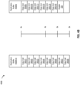
- the size of source buffers 140(1)-(N) (as well as the size of the receive/destination buffers 155(1)-(N)) in FIGs. 3A - 3E and 4A - 4C is 8k and the data is 4k aligned.
- source buffers 140(1)-(N) and destination buffers 155(1)-(N) can be any size (e.g., 16k, 32k, and the like), and the page boundary alignment of the data can also differ (e.g., the data can be 2k, 3k, or 6k aligned).
- data e.g., data units 305(1)-(13)
- a header e.g., header 235
- the data is 13k (e.g., data units 305(1)-(13)) and the header is 1k (e.g., header 235).
- the data e.g., 13k of data that is 4k page boundary aligned
- header 235 will require a separate and additional buffer (e.g., destination buffer 155(3)). Therefore, although there is no on-wire wastage, the RDMA write operation would consume three destination buffers. Consequently, three RDMA writes would be required as part of the RDMA transfer of the data and the header.
- FIG. 3B is a block diagram of a header that is written at the start of a buffer, according to one embodiment.
- the header e.g., header 235
- the start of a buffer e.g., destination buffer 140(1).
- applications in RDMA computing environments typically require the data to be written at a page boundary (e.g., at 0k or 4k in an 8k buffer, if the data is 4k page boundary aligned).
- writing the header at the start of a buffer can cause wastage on-wire between the end of the header and the start of the data, because the data has to start at a page aligned boundary (e.g., data unit 305(1) has to start at the 4k page boundary), and the number of buffers required has also not been reduced (e.g., three buffers).
- a page aligned boundary e.g., data unit 305(1) has to start at the 4k page boundary
- the number of buffers required has also not been reduced (e.g., three buffers).
- FIG. 3C is a block diagram of a header that is written immediately after data, according to one embodiment.
- writing 13k of data e.g., data units 305(1)-(13)
- two buffers e.g., destination buffers 155(1) and 155(2)
- header 235 is written immediately after the data (e.g., after data unit 305(13)).
- the OFED API provides programmers a 32-bit space with every RDMA write for private use. Destination computing system 145 can use this 32-bit value to locate appropriate buffer(s) and use information regarding the buffer(s) (e.g., the RDMA write) for further processing.
- 3C results in zero wastage on-wire and uses the minimum number of destination buffers, such a solution may not be feasible because representing the header offset (e.g., particularly if the header is not written at a header boundary) requires too many bits from the 32-bit data space.
- FIG. 3D is a block diagram of a 32-bit data space provided by the OFED API, according to one embodiment.
- 32-bit immediate data 310 contains information including a buffer identifier 315, flag(s) 320, metadata 325, a source identifier 330, a client identifier 335, and free bits 340(1)-(N) (e.g., available for header offset representation).
- Information regarding the buffer identifier, flag(s), metadata, source identifier and client identifier in addition to other information, takes up most of the space (e.g., bits) of 32-bit immediate data 310. Therefore, free bits 340(1)-(N) represent a small number of bits available for header offset representation.
- the header is written at a header boundary (e.g., so that the header offset information can be fully and accurately represented using free bits 340(1)-(N)).
- FIG. 3E is a block diagram of a header that is written at the end of an alignment, according to one embodiment.
- header 235 is written at the end of a particular alignment (e.g., at the end of a 2k alignment) and at a header boundary (e.g., at 6k in an 8k buffer).
- the alignment of header 235 is determined based on the number of bits that would potentially be available (e.g., for header placement) if the data were to be written (e.g., to one or more buffers like destination buffers 155(1) and 155(2)). The more free bits that are available, the lesser the wastage.
- the header e.g., aligned at 2k
- four possible offsets e.g., 0k, 2k, 4k, and 6k in an 8k buffer.
- the maximum possible on-wire wastage is 2k.
- the header e.g., aligned at 1k
- writing a header at the end of an alignment as shown in FIG. 3E also produces some wastage, however minimal (e.g., as compared to writing the header at the beginning of a buffer as shown in FIG. 3A ).
- FIG. 4A is a block diagram of a header that is written at the end of an alignment in a second to last buffer, according to one embodiment.
- header 235 is written in a second to last buffer (e.g., destination buffer 140(N-1)) at the last (available) header-aligned offset (e.g., of destination buffer 155(N-1)) (e.g., 6k), based on the header size (e.g., 1k as shown in FIG. 4A ) and alignment (e.g., based on a header boundary).
- a second to last buffer e.g., destination buffer 140(N-1)
- the last (available) header-aligned offset e.g., of destination buffer 155(N-1)
- 6k e.g., 6k
- buffer selector 215 identifies destination buffer 155(N-1) as the second to last buffer, and selects destination buffer 155(N-1) for header placement.
- Page boundary alignment calculator 225 then calculates the page boundary alignment of data that can be written to destination buffer 155(N-1) (e.g., data units 305(1)-305(6)), while data and header coalescer 220 ensures that enough space is available for header placement (e.g., 1k), header representation (e.g., in 32-bit immediate data 310), and header alignment (e.g., at 6k).
- FIG. 4A is a block diagram of a header that is written at the end of an alignment without (requiring) additional buffers, according to other embodiments. not encompassed by the wording of the claims.
- header 235 can be written after the data (e.g., after 14 data units). It will be appreciated that header and data placement in this example causes no wastage on-wire and also does not require additional (destination) buffers.
- FIG. 4C is a block diagram of a header that is written to a second to last buffer, according to one embodiment.
- header 235 is written to destination buffer 155(N-1), which is the second to last buffer.
- Header 235 as required by the need to include the header offset in 32-bit immediate data 310, is header aligned at a header boundary (e.g., at 6k).
- the available space in the last buffer is fully filled with data (e.g., data units 305(7)-(14)).
- Data units 305(1)-(6) are written to destination buffer 155(N-1).
- the data in both destination buffers 155(N-1) and 155(N) is page boundary aligned and header 235 is also aligned at a header boundary. Therefore, in this example, the minimum number of buffers required to write the data and the header are used, and there is no on-wire wastage.
- FIG. 5A is a flowchart that illustrates a process for filling buffers with data and a header, according to one embodiment.
- the process begins at 505 by receiving a header (e.g., header 235) and data (e.g., data units 305(1)-(14)), for example, as an input parameter from a host, a virtual machine, or some other type of computing system communicatively coupled to source computing system 105, or from one or more applications executing on source computing system 105.
- the process determines the number of buffers that are required for the header and the data (e.g., by using buffer selector 215 and based on the size of data units received as part of the data).
- the process page (boundary) aligns the data (e.g., by using page boundary alignment calculator 225) and records this mapping.
- the process determines whether there are data-only buffers to fill (e.g., write data (units) to). If there are data-only buffers to fill, the process at 525, fills buffer(s) with data (e.g., destination buffers 155(1)-(N-2)). If there are no data-only buffers to fill, the process, at 530, determines the position of the header on the second to last buffer (e.g., destination buffer 155(N-1)). At 535, the process fills the data up to destination buffer 155(N-2). At 540, the process fills the data and the header in destination buffer 155(N-1) (e.g., as shown in FIGs. 4A and 4C ). At 545, the process fills the last buffer (e.g., destination buffer 155(N)) with the remaining data. The process ends at 550 by determining if there is another message to process.
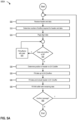
- FIG. 5B is a flowchart that illustrates a process for combining a header and data, according to one embodiment.
- the process begins at 555 by receiving data and a header contained in source buffers.
- the process initiates header and data placement analysis (e.g., using RDMA module 210).
- the process calculates the size of available buffers (e.g., 8k, 16k, 32k, and the like).
- the process determines the number (e.g., minimum) of buffers that are required for data and the header (e.g., based on the size of the data units received).
- the process determines the page boundary alignment for the data within the identified buffers (e.g., using page boundary alignment calculator 225). It should be noted that page boundary alignment calculator 225 also determines header boundaries for the header.
- the process determines the position of the header in the second to last buffer (e.g., in destination buffer 155(N-1)).
- the process determines the position of header 235 in destination buffer 155(N-1) at the end of page boundary aligned data (e.g., after data unit 305(6) as shown in FIGs. 4A and 4C ) and at a header boundary (e.g., starting at 6k for a 2k alignment of a 1k header, also as shown in FIGs. 4A and 4C ).
- the process fills destination buffers with the data and the header such that the minimum number of destination buffers are utilized and the data is page boundary aligned.
- the process sends the combined header and data along with placement/mapping information in a single RDMA write (e.g., a message sent over RDMA) to a destination (e.g., destination computing system 145).
- a destination e.g., destination computing system 145.
- the process ends at 595 by determining if there is another header and (more) data to process.
- FIG. 6 is a flowchart that illustrates a process for determining placement/mapping information of a header and data, according to one embodiment.
- the process begins at 605 by receiving data and a header.
- the process determines the minimum number of buffers required to write the data and the header.
- the process determines the placement of the data and the header in selected buffers.
- the process determines whether the data is page boundary aligned and whether the data has a minimum number of gaps that can cause on-wire wastage.
- the process at 625, re-determines placement of the data and the header in the selected buffers to keep the data page boundary aligned and with minimum (or zero) gaps.
- the process at 630, fills the selected buffers with the data and the header (e.g., as shown in FIGs. 4A and 4C ). The process ends at 635 by determining if there is another header and (more) data to process.
- FIG. 7 is a flowchart that illustrates a process for generating and transmitting data and a header using RDMA, according to one embodiment.
- the process begins at 705 by receiving or accessing data and a header (e.g., from source buffers).
- the process writes the data and the header to buffers such that the minimum number of buffers are used, the data is page boundary aligned, the header is aligned, and there is minimum (or no) on-wire wastage.
- the process includes header offset information (e.g., the location of the header if and when the header is written to a particular destination buffer) in 32-bit immediate data 310 (e.g., the 32-bit data space provided as part of API 205).
- the process generates an RDMA write (e.g., using RDMA module 210).
- the process transmits the RDMA write to a destination along with 32-bit immediate data 310 (e.g., to destination computing system 145).
- the process ends at 730 by determining if there is another header and (more) data to process.
- coalescing a header and data by mapping source buffers to one or more destination buffer(s), and writing the header and the data to particularly selected destination buffer(s) based on determined placement/mapping information results in efficient utilization of destination buffers and reduces (or even eliminates) on-wire wastage in OFED-based and RDMA-enabled computing environments. It will also be appreciated that the systems, methods, and processes described herein can also provide increased I/O performance and application throughput in such computing environments.
- FIG. 8 is a block diagram of a computing system, illustrating how a placement and mapping information module 865 can be implemented in software, according to one embodiment.
- Computing system 800 broadly represents any single or multi-processor computing device or system capable of executing computer-readable instructions. Examples of computing system 800 include, without limitation, any one or more of a variety of devices including workstations, personal computers, laptops, client-side terminals, servers, distributed computing systems, handheld devices (e.g., personal digital assistants and mobile phones), network appliances, storage controllers (e.g., array, tape drive, or hard drive controllers), and the like.
- Computing system 800 includes at least one processor 855 (e.g., source processor 110 or destination processor 175) and a memory 860 (e.g., source memory 120 or destination memory 150). By executing the software that implements source computing system 105 or destination computing system 145, computing system 800 becomes a special purpose computing device that is configured to improve throughput in OpenFabrics environments.
- Processor 855 generally represents any type or form of processing unit capable of processing data or interpreting and executing instructions. In certain embodiments, processor 855 receives instructions from a software application or module. These instructions cause processor 855 to perform the functions of one or more of the embodiments described and/or illustrated herein. Processor 855 performs and/or is a means for performing all or some of the operations described herein. Processor 855 also performs and/or is a means for performing any other operations, methods, or processes described and/or illustrated herein.
- Memory 860 generally represents any type or form of volatile or non-volatile storage devices or mediums capable of storing data and/or other computer-readable instructions. Examples include, without limitation, random access memory (RAM), read only memory (ROM), flash memory, or any other suitable memory device. Although not required, in certain embodiments computing system 800 may include both a volatile memory unit and a non-volatile storage device. In one example, program instructions implementing placement and mapping information module 865 may be loaded into memory 860 (e.g., source memory 120).
- computing system 800 may also include one or more components or elements in addition to processor 855 and/or memory 860.
- computing system 800 may include a memory controller 820, an Input/Output (I/O) controller 835, and a communication interface 845, each of which may be interconnected via a communication infrastructure 805.
- Communication infrastructure 805 generally represents any type or form of infrastructure capable of facilitating communication between one or more components of a computing device. Examples of communication infrastructure 805 include, without limitation, a communication bus (such as an Industry Standard Architecture (ISA), Peripheral Component Interconnect (PCI), PCI express (PCIe), or similar bus) and a network.
- ISA Industry Standard Architecture
- PCI Peripheral Component Interconnect
- PCIe PCI express
- Memory controller 820 generally represents any type/form of device capable of handling memory or data or controlling communication between one or more components of computing system 800. In certain embodiments memory controller 820 may control communication between processor 855, memory 860, and I/O controller 835 via communication infrastructure 805. In certain embodiments, memory controller 820 may perform and/or be a means for performing, either alone or in combination with other elements, one or more of the operations or features described and/or illustrated herein.
- I/O controller 835 generally represents any type or form of module capable of coordinating and/or controlling the input and output functions of a virtual machine, an appliance, a gateway, and/or a computing system.
- I/O controller 835 may control or facilitate transfer of data between one or more elements of source computing system 105 or destination computing system 145, such as processor 855 (e.g., source processor 110 or destination processor 175), memory 860 (e.g., source memory 120 or destination memory 150), communication interface 845, display adapter 815, input interface 825, and storage interface 840.
- processor 855 e.g., source processor 110 or destination processor 175
- memory 860 e.g., source memory 120 or destination memory 150
- communication interface 845 e.g., display adapter 815, input interface 825, and storage interface 840.
- Communication interface 845 broadly represents any type or form of communication device or adapter capable of facilitating communication between computing system 800 and one or more other devices. Communication interface 845 may facilitate communication between computing system 800 and a private or public network including additional computing systems. Examples of communication interface 845 include, without limitation, a wired network interface (such as a network interface card), a wireless network interface (such as a wireless network interface card), a modem, and any other suitable interface.
- a wired network interface such as a network interface card
- a wireless network interface such as a wireless network interface card
- modem any other suitable interface.
- Communication interface 845 may provide a direct connection to a remote server via a direct link to a network, such as the Internet, and may also indirectly provide such a connection through, for example, a local area network (e.g., an Ethernet network), a personal area network, a telephone or cable network, a cellular telephone connection, a satellite data connection, or any other suitable connection.
- a local area network e.g., an Ethernet network
- a personal area network e.g., a personal area network
- a telephone or cable network e.g., a personal area network
- a cellular telephone connection e.g., cellular telephone connection
- satellite data connection e.g., satellite data connection
- Communication interface 845 may also represent a host adapter configured to facilitate communication between computing system 800 and one or more additional network or storage devices via an external bus or communications channel.
- host adapters include, Small Computer System Interface (SCSI) host adapters, Universal Serial Bus (USB) host adapters, Institute of Electrical and Electronics Engineers (IEEE) 1394 host adapters, Serial Advanced Technology Attachment (SATA), Serial Attached SCSI (SAS), and external SATA (eSATA) host adapters, Advanced Technology Attachment (ATA) and Parallel ATA (PATA) host adapters, Fibre Channel interface adapters, Ethernet adapters, or the like.
- Communication interface 845 may also allow computing system 800 to engage in distributed or remote computing (e.g., by receiving/sending instructions to/from a remote device for execution).
- computing system 800 may also include at least one display device 810 coupled to communication infrastructure 805 via a display adapter 815.
- Display device 810 generally represents any type or form of device capable of visually displaying information forwarded by display adapter 815.
- display adapter 815 generally represents any type or form of device configured to forward graphics, text, and other data from communication infrastructure 805 (or from a frame buffer, as known in the art) for display on display device 810.
- Computing system 800 may also include at least one input device 830 coupled to communication infrastructure 805 via an input interface 825.
- Input device 830 generally represents any type or form of input device capable of providing input, either computer or human generated, to computing system 800. Examples of input device 830 include a keyboard, a pointing device, a speech recognition device, or any other input device.
- Computing system 800 may also include storage device 850 coupled to communication infrastructure 805 via a storage interface 840.
- Storage device 850 generally represents any type or form of storage devices or mediums capable of storing data and/or other computer-readable instructions.
- storage device 850 may include a magnetic disk drive (e.g., a so-called hard drive), a floppy disk drive, a magnetic tape drive, an optical disk drive, a flash drive, or the like.
- Storage interface 840 generally represents any type or form of interface or device for transferring and/or transmitting data between storage device 850, and other components of computing system 800.
- Storage device 850 may be configured to read from and/or write to a removable storage unit configured to store computer software, data, or other computer-readable information. Examples of suitable removable storage units include a floppy disk, a magnetic tape, an optical disk, a flash memory device, or the like. Storage device 850 may also include other similar structures or devices for allowing computer software, data, or other computer-readable instructions to be loaded into computing system 800. For example, storage device 850 may be configured to read and write software, data, or other computer-readable information. Storage device 850 may also be a part of computing system 800 or may be separate devices accessed through other interface systems.
- computing system 800 may be connected to computing system 800. Conversely, all of the components and devices illustrated in FIG. 8 need not be present to practice the embodiments described and/or illustrated herein. The devices and subsystems referenced above may also be interconnected in different ways from that shown in FIG. 8 .
- Computing system 800 may also employ any number of software, firmware, and/or hardware configurations.
- One or more of the embodiments disclosed herein are encoded as a computer program (also referred to as computer software, software applications, computer-readable instructions, or computer control logic) on a computer-readable storage medium.
- Examples of computer-readable storage media include magnetic-storage media (e.g., hard disk drives and floppy disks), optical-storage media (e.g., CD- or DVD-ROMs), electronic-storage media (e.g., solid-state drives and flash media), and the like.
- Such computer programs can also be transferred to computing system 800 for storage in memory via a network such as the Internet or upon a carrier medium.
- the computer-readable medium containing the computer program is loaded into computing system 800. All or a portion of the computer program stored on the computer-readable medium may then be stored in memory 860 and/or various portions of storage device 850.
- a computer program loaded into computing system 800 causes processor 855 to perform and/or be a means for performing the functions of one or more of the embodiments described and/or illustrated herein. Additionally or alternatively, one or more of the embodiments described and/or illustrated herein may be implemented in firmware and/or hardware.
- computing system 800 may be configured as an application specific integrated circuit (ASIC) adapted to implement one or more of the embodiments disclosed herein.
- ASIC application specific integrated circuit
- FIG. 9 is a block diagram of a networked system, illustrating how various devices can communicate via a network, according to one embodiment.
- network-attached storage (NAS) devices may be configured to communicate with source computing system 105 and/or destination computing system 145 using various protocols, such as Network File System (NFS), Server Message Block (SMB), or Common Internet File System (CIFS).
- NFS Network File System
- SMB Server Message Block
- CIFS Common Internet File System
- Network 180 generally represents any type or form of computer network or architecture capable of facilitating communication between source computing system 105 and/or destination computing system 145.
- a communication interface such as communication interface 845 in FIG. 8
- network 180 can be a Storage Area Network (SAN).
- SAN Storage Area Network
- all or a portion of one or more of the disclosed embodiments is encoded as a computer program and loaded onto and executed by source computing system 105 and/or destination computing system 145, or any combination thereof. All or a portion of one or more of the embodiments disclosed herein is also encoded as a computer program, stored on source computing system 105 and/or destination computing system 145, and distributed over network 180. In some examples, all or a portion of source computing system 105 and/or destination computing system 145 may represent portions of a cloud-computing or network-based environment. Cloud-computing environments may provide various services and applications via the Internet.
- cloud-based services e.g., software as a service, platform as a service, infrastructure as a service, etc.
- cloud-based services may be accessible through a web browser or other remote interface.
- Various functions described herein may be provided through a remote desktop environment or any other cloud-based computing environment.
- placement and mapping information module 865 may transform the behavior of source computing system 105 and/or destination computing system 145 in order to cause source computing system 105 and/or destination computing system 145 to improve throughput in OpenFabrics and RDMA computing environments.
Landscapes
- Engineering & Computer Science (AREA)
- Theoretical Computer Science (AREA)
- Physics & Mathematics (AREA)
- General Engineering & Computer Science (AREA)
- General Physics & Mathematics (AREA)
- Human Computer Interaction (AREA)
- Computer Networks & Wireless Communication (AREA)
- Signal Processing (AREA)
- Bus Control (AREA)
- Information Retrieval, Db Structures And Fs Structures Therefor (AREA)
- Information Transfer Systems (AREA)
Claims (9)
- Procédé, réalisé par un système, comprenant :la réception de données et d'un en-tête au niveau du système, le système nécessitant que les données soient alignées sur des limites de page ;l'identification d'une pluralité de tampons dans lesquels les données et l'en-tête doivent être écrits ;le procédé étant caractérisé en ce qu'il comprend :l'agrégation de l'en-tête et des données dans une écriture par accès mémoire direct à distance, RDMA,l'écriture RDMA comprenant un espace de données 32 bits comprenant un certain nombre de bits libres, les bits libres étant les bits de l'espace de données 32 bits qui sont disponibles pour stocker un décalage, etl'agrégation de l'en-tête et des données dans l'écriture RDMA comprenant :le mappage de l'en-tête et des données dans les tampons ;la détermination d'un nombre maximal de décalages susceptibles d'être représentés avec le nombre de bits libres, etla détermination d'un alignement de l'en-tête dans un avant-dernier tampon des tampons,l'alignement étant calculé par division d'une taille de tampon par le nombre maximal de décalages,la taille de tampon étant une taille de chacun des tampons, etl'alignement définissant une ou plusieurs limites d'en-tête ; etl'écriture des données et de l'en-tête dans les tampons par réalisation de l'écriture RDMA, l'écriture des données et de l'en-tête comprenant l'écriture des données sur des limites de page,l'écriture de l'en-tête sur une dernière limite d'en-tête de l'avant-dernier tampon, la dernière limite d'en-tête étant une dernière limite d'en-tête disponible des une ou plusieurs limites d'en-tête dans l'avant-dernier tampon, etl'écriture, dans les bits libres dans l'espace de données 32 bits, d'un décalage de la dernière limite d'en-tête des une ou plusieurs limites d'en-tête.
- Procédé selon la revendication 1, comprenant en outre :la détermination du nombre minimal de tampons nécessaires à l'écriture des données et de l'en-tête sur la base d'une taille de chaque tampon ;la détermination si l'alignement des données sur des limites de page est impossible ; etsur la base de la détermination, la sélection d'un ou de plusieurs tampons additionnels.
- Procédé selon la revendication 2, dans lequel le nombre minimal de tampons comprend un ou plusieurs tampons de destination.
- Procédé selon la revendication 1, dans lequel le mappage des données et de l'en-tête dans la pluralité de tampons est basé, au moins en partie, sur des informations de placement pour les données et l'en-tête, et le procédé comprenant en outre :
la détermination des informations de placement, les informations de placement étant déterminées sur la base, au moins en partie, de :une taille de chacun des tampons,un alignement des données sur des limites de page, etles une ou plusieurs limites d'en-tête. - Support de stockage lisible par ordinateur, CRSM, non transitoire, comprenant des instructions de programme qui, lorsqu'elles sont exécutées par un système ordinateur, amènent le système ordinateur à mettre en œuvre les étapes d'un procédé selon l'une quelconque des revendications 1 à 4.
- Système ordinateur, comprenant :un ou plusieurs processeurs ; etune mémoire couplée aux un ou plusieurs processeurs, la mémoire stockant des instructions de programme exécutables par les un ou plusieurs processeurs pour :recevoir des données et un en-tête au niveau du système ordinateur, le système ordinateur nécessitant que les données soient alignées sur des limites de page ;identifier une pluralité de tampons dans lesquels les données et l'en-tête doivent être écrits ;caractérisé en ce que les instructions de programme sont exécutables pour :agréger l'en-tête et les données dans une écriture par accès mémoire direct à distance (RDMA),l'écriture RDMA comprenant un espace de données 32 bits comprenant un certain nombre de bits libres, les bits libres étant les bits de l'espace de données 32 bits qui sont disponibles pour stocker un décalage, etl'en-tête et les données étant agrégés dans l'écriture RDMA parmappage de l'en-tête et des données dans les tampons ;détermination d'un nombre maximal de décalages susceptibles d'être représentés avec le nombre de bits libres, etdétermination d'un alignement de l'en-tête dans un avant-dernier tampon des tampons,l'alignement étant calculé par division d'une taille de tampon par le nombre maximal de décalages,la taille de tampon étant une taille de chacun des tampons, etl'alignement définissant une ou plusieurs limites d'en-tête ; etécrire les données et l'en-tête dans les tampons en réalisant l'écriture RDMA, les données et l'en-tête étant écrits dans les tampons par :écriture des données sur des limites de page,écriture de l'en-tête sur une dernière limite d'en-tête de l'avant-dernier tampon, la dernière limite d'en-tête étant une dernière limite d'en-tête disponible des une ou plusieurs limites d'en-tête dans l'avant-dernier tampon, etécriture, dans les bits libres dans l'espace de données 32 bits, d'un décalage de la dernière limite d'en-tête des une ou plusieurs limites d'en-tête.
- Système ordinateur selon la revendication 6, dans lequel le mappage des données et de l'en-tête dans la pluralité de tampons est basé, au moins en partie, sur des informations de placement pour les données et l'en-tête, et les instructions de programme sont exécutables en outre par les un ou plusieurs processeurs pour :
déterminer les informations de placement,
les informations de placement étant déterminées sur la base, au moins en partie, de :une taille de chacun des tampons,un alignement des données sur des limites de page, etles une ou plusieurs limites d'en-tête. - Système ordinateur selon l'une quelconque des revendications 6 ou 7, dans lequel les instructions de programme sont exécutables en outre par les un ou plusieurs processeurs pour :déterminer le nombre minimal de tampons nécessaires à l'écriture des données et de l'en-tête sur la base d'une taille de chaque tampon ;déterminer si l'alignement des données sur des limites de page est impossible ; etsur la base de la détermination, sélectionner un ou plusieurs tampons additionnels.
- Système ordinateur selon l'une quelconque des revendications 7 à 8, dans lequel un nombre minimal de tampons comprend un ou plusieurs tampons de destination.
Applications Claiming Priority (2)
| Application Number | Priority Date | Filing Date | Title |
|---|---|---|---|
| US15/168,449 US10375168B2 (en) | 2016-05-31 | 2016-05-31 | Throughput in openfabrics environments |
| PCT/US2017/033951 WO2017210015A1 (fr) | 2016-05-31 | 2017-05-23 | Amélioration du débit dans des environnements openfabrics |
Publications (2)
| Publication Number | Publication Date |
|---|---|
| EP3465450A1 EP3465450A1 (fr) | 2019-04-10 |
| EP3465450B1 true EP3465450B1 (fr) | 2023-07-26 |
Family
ID=59215982
Family Applications (1)
| Application Number | Title | Priority Date | Filing Date |
|---|---|---|---|
| EP17733209.5A Active EP3465450B1 (fr) | 2016-05-31 | 2017-05-23 | Amélioration du débit dans des environnements openfabrics |
Country Status (5)
| Country | Link |
|---|---|
| US (1) | US10375168B2 (fr) |
| EP (1) | EP3465450B1 (fr) |
| JP (1) | JP6788691B2 (fr) |
| CN (1) | CN109478171B (fr) |
| WO (1) | WO2017210015A1 (fr) |
Families Citing this family (6)
| Publication number | Priority date | Publication date | Assignee | Title |
|---|---|---|---|---|
| US9996463B2 (en) * | 2015-11-10 | 2018-06-12 | International Business Machines Corporation | Selection and placement of volumes in a storage system using stripes |
| CN110888827B (zh) * | 2018-09-10 | 2021-04-09 | 华为技术有限公司 | 数据传输方法、装置、设备及存储介质 |
| US11379404B2 (en) * | 2018-12-18 | 2022-07-05 | Sap Se | Remote memory management |
| US11863469B2 (en) * | 2020-05-06 | 2024-01-02 | International Business Machines Corporation | Utilizing coherently attached interfaces in a network stack framework |
| US20220299973A1 (en) * | 2021-03-19 | 2022-09-22 | GM Global Technology Operations LLC | Manufacturing system throughput bottleneck indicator analysis |
| US20240305685A1 (en) * | 2023-03-10 | 2024-09-12 | Nvidia Corporation | Dynamic transport protocol switching for collaborative content creation and distributed content experience systems and applications |
Family Cites Families (14)
| Publication number | Priority date | Publication date | Assignee | Title |
|---|---|---|---|---|
| EP0574140A1 (fr) * | 1992-05-29 | 1993-12-15 | Hewlett-Packard Company | Adapteur de réseau plaçant une en-tête réseau et des données dans des tampons mémoire différents |
| US5491802A (en) * | 1992-05-29 | 1996-02-13 | Hewlett-Packard Company | Network adapter for inserting pad bytes into packet link headers based on destination service access point fields for efficient memory transfer |
| WO1999034273A2 (fr) | 1997-12-30 | 1999-07-08 | Lsi Logic Corporation | Acces direct memoire de listes doubles de ventilation/regroupement automatisees |
| US6694392B1 (en) | 2000-06-30 | 2004-02-17 | Intel Corporation | Transaction partitioning |
| US7361881B2 (en) * | 2002-03-13 | 2008-04-22 | Oy Ajat Ltd | Ganged detector pixel, photon/pulse counting radiation imaging device |
| JP2004240711A (ja) * | 2003-02-06 | 2004-08-26 | Fujitsu Ltd | バッファメモリ装置及びバッファメモリ制御方法 |
| US7376763B2 (en) | 2003-07-17 | 2008-05-20 | International Business Machines Corporation | Method for transferring data from a memory subsystem to a network adapter by extending data lengths to improve the memory subsystem and PCI bus efficiency |
| US8190796B2 (en) | 2004-11-02 | 2012-05-29 | Standard Microsystems Corporation | Hardware supported peripheral component memory alignment method |
| US7590777B2 (en) * | 2004-12-10 | 2009-09-15 | International Business Machines Corporation | Transferring data between system and storage in a shared buffer |
| WO2009144800A1 (fr) * | 2008-05-29 | 2009-12-03 | 富士通株式会社 | Dispositif de relais de données, programme de relais de données, récepteur de données et système de communication |
| US8874844B1 (en) * | 2008-12-02 | 2014-10-28 | Nvidia Corporation | Padding buffer requests to avoid reads of invalid data |
| JP5482230B2 (ja) * | 2010-01-25 | 2014-05-07 | 富士通株式会社 | 通信装置、情報処理装置、通信装置の制御方法及び制御プログラム |
| US9146678B2 (en) * | 2013-04-29 | 2015-09-29 | International Business Machines Corporation | High throughput hardware acceleration using pre-staging buffers |
| US20160026605A1 (en) * | 2014-07-28 | 2016-01-28 | Emulex Corporation | Registrationless transmit onload rdma |
-
2016
- 2016-05-31 US US15/168,449 patent/US10375168B2/en active Active
-
2017
- 2017-05-23 CN CN201780029882.6A patent/CN109478171B/zh active Active
- 2017-05-23 EP EP17733209.5A patent/EP3465450B1/fr active Active
- 2017-05-23 WO PCT/US2017/033951 patent/WO2017210015A1/fr not_active Ceased
- 2017-05-23 JP JP2018561265A patent/JP6788691B2/ja active Active
Also Published As
| Publication number | Publication date |
|---|---|
| EP3465450A1 (fr) | 2019-04-10 |
| CN109478171B (zh) | 2022-11-15 |
| JP2019517692A (ja) | 2019-06-24 |
| CN109478171A (zh) | 2019-03-15 |
| US20170346899A1 (en) | 2017-11-30 |
| JP6788691B2 (ja) | 2020-11-25 |
| WO2017210015A1 (fr) | 2017-12-07 |
| US10375168B2 (en) | 2019-08-06 |
Similar Documents
| Publication | Publication Date | Title |
|---|---|---|
| EP3465450B1 (fr) | Amélioration du débit dans des environnements openfabrics | |
| EP2889780B1 (fr) | Système de traitement de données et procédé de traitement de données | |
| EP3057272B1 (fr) | Technologies pour la mise à jour de tableaux de consultation de flux par hachage "coucou" | |
| US9934065B1 (en) | Servicing I/O requests in an I/O adapter device | |
| EP3211530B1 (fr) | Procédé de gestion de mémoire de machine virtuelle, machine principale physique, dispositif pcie et son procédé de configuration, et dispositif de gestion de migration | |
| US10116746B2 (en) | Data storage method and network interface card | |
| CN103176833B (zh) | 一种基于虚拟机的数据发送方法、接收方法及系统 | |
| US11068399B2 (en) | Technologies for enforcing coherence ordering in consumer polling interactions by receiving snoop request by controller and update value of cache line | |
| US9727521B2 (en) | Efficient CPU mailbox read access to GPU memory | |
| EP2840576A1 (fr) | Disque dur et procede de traitement de donnees | |
| CN114817121A (zh) | 用于处理数据的方法、电子设备和计算机程序产品 | |
| CN103678203A (zh) | 一种实现网卡零拷贝方法及装置 | |
| CN111881476B (zh) | 对象存储控制方法、装置、计算机设备及存储介质 | |
| JP5893028B2 (ja) | キャッシングに対応したストレージ装置上における効率的なシーケンシャルロギングのためのシステム及び方法 | |
| US10581997B2 (en) | Techniques for storing or accessing a key-value item | |
| US10523741B2 (en) | System and method for avoiding proxy connection latency | |
| US10853255B2 (en) | Apparatus and method of optimizing memory transactions to persistent memory using an architectural data mover | |
| CN113422792B (zh) | 数据传输方法、装置、电子设备及计算机存储介质 | |
| CN107908365A (zh) | 用户态存储系统数据交互的方法、装置及设备 | |
| US10367886B2 (en) | Information processing apparatus, parallel computer system, and file server communication program | |
| CN105988871B (zh) | 一种远端内存分配方法、装置和系统 | |
| CN108228078A (zh) | 用于存储系统中的数据访问方法和装置 | |
| CN114063891B (zh) | 管理数据传输的方法、设备和计算机程序产品 | |
| CN106325377B (zh) | 外部设备扩展卡及输入输出外部设备的数据处理方法 | |
| CN119728615A (zh) | 基于指针的报文dma方法、装置及电子设备 |
Legal Events
| Date | Code | Title | Description |
|---|---|---|---|
| STAA | Information on the status of an ep patent application or granted ep patent |
Free format text: STATUS: UNKNOWN |
|
| STAA | Information on the status of an ep patent application or granted ep patent |
Free format text: STATUS: THE INTERNATIONAL PUBLICATION HAS BEEN MADE |
|
| PUAI | Public reference made under article 153(3) epc to a published international application that has entered the european phase |
Free format text: ORIGINAL CODE: 0009012 |
|
| STAA | Information on the status of an ep patent application or granted ep patent |
Free format text: STATUS: REQUEST FOR EXAMINATION WAS MADE |
|
| 17P | Request for examination filed |
Effective date: 20181220 |
|
| AK | Designated contracting states |
Kind code of ref document: A1 Designated state(s): AL AT BE BG CH CY CZ DE DK EE ES FI FR GB GR HR HU IE IS IT LI LT LU LV MC MK MT NL NO PL PT RO RS SE SI SK SM TR |
|
| AX | Request for extension of the european patent |
Extension state: BA ME |
|
| DAV | Request for validation of the european patent (deleted) | ||
| DAX | Request for extension of the european patent (deleted) | ||
| STAA | Information on the status of an ep patent application or granted ep patent |
Free format text: STATUS: EXAMINATION IS IN PROGRESS |
|
| 17Q | First examination report despatched |
Effective date: 20191007 |
|
| GRAP | Despatch of communication of intention to grant a patent |
Free format text: ORIGINAL CODE: EPIDOSNIGR1 |
|
| STAA | Information on the status of an ep patent application or granted ep patent |
Free format text: STATUS: GRANT OF PATENT IS INTENDED |
|
| INTG | Intention to grant announced |
Effective date: 20220816 |
|
| GRAJ | Information related to disapproval of communication of intention to grant by the applicant or resumption of examination proceedings by the epo deleted |
Free format text: ORIGINAL CODE: EPIDOSDIGR1 |
|
| STAA | Information on the status of an ep patent application or granted ep patent |
Free format text: STATUS: EXAMINATION IS IN PROGRESS |
|
| INTC | Intention to grant announced (deleted) | ||
| GRAP | Despatch of communication of intention to grant a patent |
Free format text: ORIGINAL CODE: EPIDOSNIGR1 |
|
| STAA | Information on the status of an ep patent application or granted ep patent |
Free format text: STATUS: GRANT OF PATENT IS INTENDED |
|
| INTG | Intention to grant announced |
Effective date: 20230214 |
|
| GRAS | Grant fee paid |
Free format text: ORIGINAL CODE: EPIDOSNIGR3 |
|
| GRAA | (expected) grant |
Free format text: ORIGINAL CODE: 0009210 |
|
| STAA | Information on the status of an ep patent application or granted ep patent |
Free format text: STATUS: THE PATENT HAS BEEN GRANTED |
|
| P01 | Opt-out of the competence of the unified patent court (upc) registered |
Effective date: 20230523 |
|
| AK | Designated contracting states |
Kind code of ref document: B1 Designated state(s): AL AT BE BG CH CY CZ DE DK EE ES FI FR GB GR HR HU IE IS IT LI LT LU LV MC MK MT NL NO PL PT RO RS SE SI SK SM TR |
|
| REG | Reference to a national code |
Ref country code: CH Ref legal event code: EP |
|
| REG | Reference to a national code |
Ref country code: IE Ref legal event code: FG4D |
|
| REG | Reference to a national code |
Ref country code: DE Ref legal event code: R096 Ref document number: 602017071782 Country of ref document: DE |
|
| REG | Reference to a national code |
Ref country code: LT Ref legal event code: MG9D |
|
| REG | Reference to a national code |
Ref country code: NL Ref legal event code: MP Effective date: 20230726 |
|
| REG | Reference to a national code |
Ref country code: AT Ref legal event code: MK05 Ref document number: 1592735 Country of ref document: AT Kind code of ref document: T Effective date: 20230726 |
|
| PG25 | Lapsed in a contracting state [announced via postgrant information from national office to epo] |
Ref country code: NL Free format text: LAPSE BECAUSE OF FAILURE TO SUBMIT A TRANSLATION OF THE DESCRIPTION OR TO PAY THE FEE WITHIN THE PRESCRIBED TIME-LIMIT Effective date: 20230726 |
|
| PG25 | Lapsed in a contracting state [announced via postgrant information from national office to epo] |
Ref country code: GR Free format text: LAPSE BECAUSE OF FAILURE TO SUBMIT A TRANSLATION OF THE DESCRIPTION OR TO PAY THE FEE WITHIN THE PRESCRIBED TIME-LIMIT Effective date: 20231027 |
|
| PG25 | Lapsed in a contracting state [announced via postgrant information from national office to epo] |
Ref country code: IS Free format text: LAPSE BECAUSE OF FAILURE TO SUBMIT A TRANSLATION OF THE DESCRIPTION OR TO PAY THE FEE WITHIN THE PRESCRIBED TIME-LIMIT Effective date: 20231126 |
|
| PG25 | Lapsed in a contracting state [announced via postgrant information from national office to epo] |
Ref country code: SE Free format text: LAPSE BECAUSE OF FAILURE TO SUBMIT A TRANSLATION OF THE DESCRIPTION OR TO PAY THE FEE WITHIN THE PRESCRIBED TIME-LIMIT Effective date: 20230726 Ref country code: RS Free format text: LAPSE BECAUSE OF FAILURE TO SUBMIT A TRANSLATION OF THE DESCRIPTION OR TO PAY THE FEE WITHIN THE PRESCRIBED TIME-LIMIT Effective date: 20230726 Ref country code: PT Free format text: LAPSE BECAUSE OF FAILURE TO SUBMIT A TRANSLATION OF THE DESCRIPTION OR TO PAY THE FEE WITHIN THE PRESCRIBED TIME-LIMIT Effective date: 20231127 Ref country code: NO Free format text: LAPSE BECAUSE OF FAILURE TO SUBMIT A TRANSLATION OF THE DESCRIPTION OR TO PAY THE FEE WITHIN THE PRESCRIBED TIME-LIMIT Effective date: 20231026 Ref country code: LV Free format text: LAPSE BECAUSE OF FAILURE TO SUBMIT A TRANSLATION OF THE DESCRIPTION OR TO PAY THE FEE WITHIN THE PRESCRIBED TIME-LIMIT Effective date: 20230726 Ref country code: LT Free format text: LAPSE BECAUSE OF FAILURE TO SUBMIT A TRANSLATION OF THE DESCRIPTION OR TO PAY THE FEE WITHIN THE PRESCRIBED TIME-LIMIT Effective date: 20230726 Ref country code: IS Free format text: LAPSE BECAUSE OF FAILURE TO SUBMIT A TRANSLATION OF THE DESCRIPTION OR TO PAY THE FEE WITHIN THE PRESCRIBED TIME-LIMIT Effective date: 20231126 Ref country code: HR Free format text: LAPSE BECAUSE OF FAILURE TO SUBMIT A TRANSLATION OF THE DESCRIPTION OR TO PAY THE FEE WITHIN THE PRESCRIBED TIME-LIMIT Effective date: 20230726 Ref country code: GR Free format text: LAPSE BECAUSE OF FAILURE TO SUBMIT A TRANSLATION OF THE DESCRIPTION OR TO PAY THE FEE WITHIN THE PRESCRIBED TIME-LIMIT Effective date: 20231027 Ref country code: FI Free format text: LAPSE BECAUSE OF FAILURE TO SUBMIT A TRANSLATION OF THE DESCRIPTION OR TO PAY THE FEE WITHIN THE PRESCRIBED TIME-LIMIT Effective date: 20230726 Ref country code: AT Free format text: LAPSE BECAUSE OF FAILURE TO SUBMIT A TRANSLATION OF THE DESCRIPTION OR TO PAY THE FEE WITHIN THE PRESCRIBED TIME-LIMIT Effective date: 20230726 |
|
| PG25 | Lapsed in a contracting state [announced via postgrant information from national office to epo] |
Ref country code: PL Free format text: LAPSE BECAUSE OF FAILURE TO SUBMIT A TRANSLATION OF THE DESCRIPTION OR TO PAY THE FEE WITHIN THE PRESCRIBED TIME-LIMIT Effective date: 20230726 |
|
| PG25 | Lapsed in a contracting state [announced via postgrant information from national office to epo] |
Ref country code: ES Free format text: LAPSE BECAUSE OF FAILURE TO SUBMIT A TRANSLATION OF THE DESCRIPTION OR TO PAY THE FEE WITHIN THE PRESCRIBED TIME-LIMIT Effective date: 20230726 |
|
| REG | Reference to a national code |
Ref country code: DE Ref legal event code: R097 Ref document number: 602017071782 Country of ref document: DE |
|
| PG25 | Lapsed in a contracting state [announced via postgrant information from national office to epo] |
Ref country code: SM Free format text: LAPSE BECAUSE OF FAILURE TO SUBMIT A TRANSLATION OF THE DESCRIPTION OR TO PAY THE FEE WITHIN THE PRESCRIBED TIME-LIMIT Effective date: 20230726 Ref country code: RO Free format text: LAPSE BECAUSE OF FAILURE TO SUBMIT A TRANSLATION OF THE DESCRIPTION OR TO PAY THE FEE WITHIN THE PRESCRIBED TIME-LIMIT Effective date: 20230726 Ref country code: ES Free format text: LAPSE BECAUSE OF FAILURE TO SUBMIT A TRANSLATION OF THE DESCRIPTION OR TO PAY THE FEE WITHIN THE PRESCRIBED TIME-LIMIT Effective date: 20230726 Ref country code: EE Free format text: LAPSE BECAUSE OF FAILURE TO SUBMIT A TRANSLATION OF THE DESCRIPTION OR TO PAY THE FEE WITHIN THE PRESCRIBED TIME-LIMIT Effective date: 20230726 Ref country code: DK Free format text: LAPSE BECAUSE OF FAILURE TO SUBMIT A TRANSLATION OF THE DESCRIPTION OR TO PAY THE FEE WITHIN THE PRESCRIBED TIME-LIMIT Effective date: 20230726 Ref country code: CZ Free format text: LAPSE BECAUSE OF FAILURE TO SUBMIT A TRANSLATION OF THE DESCRIPTION OR TO PAY THE FEE WITHIN THE PRESCRIBED TIME-LIMIT Effective date: 20230726 Ref country code: SK Free format text: LAPSE BECAUSE OF FAILURE TO SUBMIT A TRANSLATION OF THE DESCRIPTION OR TO PAY THE FEE WITHIN THE PRESCRIBED TIME-LIMIT Effective date: 20230726 |
|
| PG25 | Lapsed in a contracting state [announced via postgrant information from national office to epo] |
Ref country code: IT Free format text: LAPSE BECAUSE OF FAILURE TO SUBMIT A TRANSLATION OF THE DESCRIPTION OR TO PAY THE FEE WITHIN THE PRESCRIBED TIME-LIMIT Effective date: 20230726 |
|
| PLBE | No opposition filed within time limit |
Free format text: ORIGINAL CODE: 0009261 |
|
| STAA | Information on the status of an ep patent application or granted ep patent |
Free format text: STATUS: NO OPPOSITION FILED WITHIN TIME LIMIT |
|
| 26N | No opposition filed |
Effective date: 20240429 |
|
| PG25 | Lapsed in a contracting state [announced via postgrant information from national office to epo] |
Ref country code: SI Free format text: LAPSE BECAUSE OF FAILURE TO SUBMIT A TRANSLATION OF THE DESCRIPTION OR TO PAY THE FEE WITHIN THE PRESCRIBED TIME-LIMIT Effective date: 20230726 |
|
| PG25 | Lapsed in a contracting state [announced via postgrant information from national office to epo] |
Ref country code: BG Free format text: LAPSE BECAUSE OF FAILURE TO SUBMIT A TRANSLATION OF THE DESCRIPTION OR TO PAY THE FEE WITHIN THE PRESCRIBED TIME-LIMIT Effective date: 20230726 |
|
| PG25 | Lapsed in a contracting state [announced via postgrant information from national office to epo] |
Ref country code: BG Free format text: LAPSE BECAUSE OF FAILURE TO SUBMIT A TRANSLATION OF THE DESCRIPTION OR TO PAY THE FEE WITHIN THE PRESCRIBED TIME-LIMIT Effective date: 20230726 |
|
| REG | Reference to a national code |
Ref country code: CH Ref legal event code: PL |
|
| PG25 | Lapsed in a contracting state [announced via postgrant information from national office to epo] |
Ref country code: MC Free format text: LAPSE BECAUSE OF FAILURE TO SUBMIT A TRANSLATION OF THE DESCRIPTION OR TO PAY THE FEE WITHIN THE PRESCRIBED TIME-LIMIT Effective date: 20230726 |
|
| PG25 | Lapsed in a contracting state [announced via postgrant information from national office to epo] |
Ref country code: LU Free format text: LAPSE BECAUSE OF NON-PAYMENT OF DUE FEES Effective date: 20240523 |
|
| PG25 | Lapsed in a contracting state [announced via postgrant information from national office to epo] |
Ref country code: MC Free format text: LAPSE BECAUSE OF FAILURE TO SUBMIT A TRANSLATION OF THE DESCRIPTION OR TO PAY THE FEE WITHIN THE PRESCRIBED TIME-LIMIT Effective date: 20230726 Ref country code: LU Free format text: LAPSE BECAUSE OF NON-PAYMENT OF DUE FEES Effective date: 20240523 Ref country code: CH Free format text: LAPSE BECAUSE OF NON-PAYMENT OF DUE FEES Effective date: 20240531 |
|
| REG | Reference to a national code |
Ref country code: BE Ref legal event code: MM Effective date: 20240531 |
|
| PG25 | Lapsed in a contracting state [announced via postgrant information from national office to epo] |
Ref country code: IE Free format text: LAPSE BECAUSE OF NON-PAYMENT OF DUE FEES Effective date: 20240523 |
|
| PG25 | Lapsed in a contracting state [announced via postgrant information from national office to epo] |
Ref country code: BE Free format text: LAPSE BECAUSE OF NON-PAYMENT OF DUE FEES Effective date: 20240531 |
|
| PGFP | Annual fee paid to national office [announced via postgrant information from national office to epo] |
Ref country code: DE Payment date: 20250529 Year of fee payment: 9 |
|
| PGFP | Annual fee paid to national office [announced via postgrant information from national office to epo] |
Ref country code: GB Payment date: 20250527 Year of fee payment: 9 |
|
| PGFP | Annual fee paid to national office [announced via postgrant information from national office to epo] |
Ref country code: FR Payment date: 20250526 Year of fee payment: 9 |
|
| PG25 | Lapsed in a contracting state [announced via postgrant information from national office to epo] |
Ref country code: CY Free format text: LAPSE BECAUSE OF FAILURE TO SUBMIT A TRANSLATION OF THE DESCRIPTION OR TO PAY THE FEE WITHIN THE PRESCRIBED TIME-LIMIT; INVALID AB INITIO Effective date: 20170523 |
|
| PG25 | Lapsed in a contracting state [announced via postgrant information from national office to epo] |
Ref country code: HU Free format text: LAPSE BECAUSE OF FAILURE TO SUBMIT A TRANSLATION OF THE DESCRIPTION OR TO PAY THE FEE WITHIN THE PRESCRIBED TIME-LIMIT; INVALID AB INITIO Effective date: 20170523 |