EP3483156A1 - Organic molecues for use in optoelectronic devices - Google Patents
Organic molecues for use in optoelectronic devices Download PDFInfo
- Publication number
- EP3483156A1 EP3483156A1 EP18204400.8A EP18204400A EP3483156A1 EP 3483156 A1 EP3483156 A1 EP 3483156A1 EP 18204400 A EP18204400 A EP 18204400A EP 3483156 A1 EP3483156 A1 EP 3483156A1
- Authority
- EP
- European Patent Office
- Prior art keywords
- optionally substituted
- substituents
- organic
- group
- weight
- Prior art date
- Legal status (The legal status is an assumption and is not a legal conclusion. Google has not performed a legal analysis and makes no representation as to the accuracy of the status listed.)
- Granted
Links
- 0 *c1cccc(c2c3cccc2)c1[n]3-c(c(*)c(*)c(C#N)c1*)c1-c1nc(-c(c(*)c(c(I)c2*)C#N)c2-[n]2c(c(*)ccc3)c3c3ccccc23)nc(-c2c(*)c(*)c(*)c(*)c2*)n1 Chemical compound *c1cccc(c2c3cccc2)c1[n]3-c(c(*)c(*)c(C#N)c1*)c1-c1nc(-c(c(*)c(c(I)c2*)C#N)c2-[n]2c(c(*)ccc3)c3c3ccccc23)nc(-c2c(*)c(*)c(*)c(*)c2*)n1 0.000 description 2
- DGTFOQQPWDUTCC-UHFFFAOYSA-N Cc(cc(c(C)c1)-c2ccc(cc3)c4c2ccc2c4c3ccc2-c2cc(-c3c(cccc4)c4c(-c(cc4)ccc4-c4c(cccc5)c5c(-c(cc5)ccc5C#N)c5c4cccc5)c4c3cccc4)ccc2OC)c1-c1ccc(cc2)c3c1ccc1cccc2c31 Chemical compound Cc(cc(c(C)c1)-c2ccc(cc3)c4c2ccc2c4c3ccc2-c2cc(-c3c(cccc4)c4c(-c(cc4)ccc4-c4c(cccc5)c5c(-c(cc5)ccc5C#N)c5c4cccc5)c4c3cccc4)ccc2OC)c1-c1ccc(cc2)c3c1ccc1cccc2c31 DGTFOQQPWDUTCC-UHFFFAOYSA-N 0.000 description 1
Images


Classifications
-
- C—CHEMISTRY; METALLURGY
- C07—ORGANIC CHEMISTRY
- C07D—HETEROCYCLIC COMPOUNDS
- C07D403/00—Heterocyclic compounds containing two or more hetero rings, having nitrogen atoms as the only ring hetero atoms, not provided for by group C07D401/00
- C07D403/14—Heterocyclic compounds containing two or more hetero rings, having nitrogen atoms as the only ring hetero atoms, not provided for by group C07D401/00 containing three or more hetero rings
-
- C—CHEMISTRY; METALLURGY
- C07—ORGANIC CHEMISTRY
- C07D—HETEROCYCLIC COMPOUNDS
- C07D471/00—Heterocyclic compounds containing nitrogen atoms as the only ring hetero atoms in the condensed system, at least one ring being a six-membered ring with one nitrogen atom, not provided for by groups C07D451/00 - C07D463/00
- C07D471/02—Heterocyclic compounds containing nitrogen atoms as the only ring hetero atoms in the condensed system, at least one ring being a six-membered ring with one nitrogen atom, not provided for by groups C07D451/00 - C07D463/00 in which the condensed system contains two hetero rings
- C07D471/04—Ortho-condensed systems
-
- C—CHEMISTRY; METALLURGY
- C07—ORGANIC CHEMISTRY
- C07D—HETEROCYCLIC COMPOUNDS
- C07D491/00—Heterocyclic compounds containing in the condensed ring system both one or more rings having oxygen atoms as the only ring hetero atoms and one or more rings having nitrogen atoms as the only ring hetero atoms, not provided for by groups C07D451/00 - C07D459/00, C07D463/00, C07D477/00 or C07D489/00
- C07D491/02—Heterocyclic compounds containing in the condensed ring system both one or more rings having oxygen atoms as the only ring hetero atoms and one or more rings having nitrogen atoms as the only ring hetero atoms, not provided for by groups C07D451/00 - C07D459/00, C07D463/00, C07D477/00 or C07D489/00 in which the condensed system contains two hetero rings
- C07D491/04—Ortho-condensed systems
- C07D491/044—Ortho-condensed systems with only one oxygen atom as ring hetero atom in the oxygen-containing ring
- C07D491/048—Ortho-condensed systems with only one oxygen atom as ring hetero atom in the oxygen-containing ring the oxygen-containing ring being five-membered
-
- C—CHEMISTRY; METALLURGY
- C07—ORGANIC CHEMISTRY
- C07D—HETEROCYCLIC COMPOUNDS
- C07D493/00—Heterocyclic compounds containing oxygen atoms as the only ring hetero atoms in the condensed system
- C07D493/02—Heterocyclic compounds containing oxygen atoms as the only ring hetero atoms in the condensed system in which the condensed system contains two hetero rings
- C07D493/04—Ortho-condensed systems
-
- C—CHEMISTRY; METALLURGY
- C07—ORGANIC CHEMISTRY
- C07D—HETEROCYCLIC COMPOUNDS
- C07D495/00—Heterocyclic compounds containing in the condensed system at least one hetero ring having sulfur atoms as the only ring hetero atoms
- C07D495/02—Heterocyclic compounds containing in the condensed system at least one hetero ring having sulfur atoms as the only ring hetero atoms in which the condensed system contains two hetero rings
- C07D495/04—Ortho-condensed systems
-
- C—CHEMISTRY; METALLURGY
- C07—ORGANIC CHEMISTRY
- C07D—HETEROCYCLIC COMPOUNDS
- C07D519/00—Heterocyclic compounds containing more than one system of two or more relevant hetero rings condensed among themselves or condensed with a common carbocyclic ring system not provided for in groups C07D453/00 or C07D455/00
-
- C—CHEMISTRY; METALLURGY
- C09—DYES; PAINTS; POLISHES; NATURAL RESINS; ADHESIVES; COMPOSITIONS NOT OTHERWISE PROVIDED FOR; APPLICATIONS OF MATERIALS NOT OTHERWISE PROVIDED FOR
- C09K—MATERIALS FOR MISCELLANEOUS APPLICATIONS, NOT PROVIDED FOR ELSEWHERE
- C09K11/00—Luminescent materials, e.g. electroluminescent or chemiluminescent
- C09K11/06—Luminescent materials, e.g. electroluminescent or chemiluminescent containing organic luminescent materials
-
- H—ELECTRICITY
- H10—SEMICONDUCTOR DEVICES; ELECTRIC SOLID-STATE DEVICES NOT OTHERWISE PROVIDED FOR
- H10K—ORGANIC ELECTRIC SOLID-STATE DEVICES
- H10K30/00—Organic devices sensitive to infrared radiation, light, electromagnetic radiation of shorter wavelength or corpuscular radiation
- H10K30/80—Constructional details
-
- H—ELECTRICITY
- H10—SEMICONDUCTOR DEVICES; ELECTRIC SOLID-STATE DEVICES NOT OTHERWISE PROVIDED FOR
- H10K—ORGANIC ELECTRIC SOLID-STATE DEVICES
- H10K50/00—Organic light-emitting devices
- H10K50/10—OLEDs or polymer light-emitting diodes [PLED]
- H10K50/18—Carrier blocking layers
-
- H—ELECTRICITY
- H10—SEMICONDUCTOR DEVICES; ELECTRIC SOLID-STATE DEVICES NOT OTHERWISE PROVIDED FOR
- H10K—ORGANIC ELECTRIC SOLID-STATE DEVICES
- H10K50/00—Organic light-emitting devices
- H10K50/30—Organic light-emitting transistors
-
- H—ELECTRICITY
- H10—SEMICONDUCTOR DEVICES; ELECTRIC SOLID-STATE DEVICES NOT OTHERWISE PROVIDED FOR
- H10K—ORGANIC ELECTRIC SOLID-STATE DEVICES
- H10K85/00—Organic materials used in the body or electrodes of devices covered by this subclass
- H10K85/60—Organic compounds having low molecular weight
- H10K85/649—Aromatic compounds comprising a hetero atom
- H10K85/654—Aromatic compounds comprising a hetero atom comprising only nitrogen as heteroatom
-
- H—ELECTRICITY
- H10—SEMICONDUCTOR DEVICES; ELECTRIC SOLID-STATE DEVICES NOT OTHERWISE PROVIDED FOR
- H10K—ORGANIC ELECTRIC SOLID-STATE DEVICES
- H10K85/00—Organic materials used in the body or electrodes of devices covered by this subclass
- H10K85/60—Organic compounds having low molecular weight
- H10K85/649—Aromatic compounds comprising a hetero atom
- H10K85/657—Polycyclic condensed heteroaromatic hydrocarbons
- H10K85/6572—Polycyclic condensed heteroaromatic hydrocarbons comprising only nitrogen in the heteroaromatic polycondensed ring system, e.g. phenanthroline or carbazole
-
- C—CHEMISTRY; METALLURGY
- C09—DYES; PAINTS; POLISHES; NATURAL RESINS; ADHESIVES; COMPOSITIONS NOT OTHERWISE PROVIDED FOR; APPLICATIONS OF MATERIALS NOT OTHERWISE PROVIDED FOR
- C09K—MATERIALS FOR MISCELLANEOUS APPLICATIONS, NOT PROVIDED FOR ELSEWHERE
- C09K2211/00—Chemical nature of organic luminescent or tenebrescent compounds
- C09K2211/10—Non-macromolecular compounds
- C09K2211/1003—Carbocyclic compounds
- C09K2211/1007—Non-condensed systems
-
- C—CHEMISTRY; METALLURGY
- C09—DYES; PAINTS; POLISHES; NATURAL RESINS; ADHESIVES; COMPOSITIONS NOT OTHERWISE PROVIDED FOR; APPLICATIONS OF MATERIALS NOT OTHERWISE PROVIDED FOR
- C09K—MATERIALS FOR MISCELLANEOUS APPLICATIONS, NOT PROVIDED FOR ELSEWHERE
- C09K2211/00—Chemical nature of organic luminescent or tenebrescent compounds
- C09K2211/10—Non-macromolecular compounds
- C09K2211/1018—Heterocyclic compounds
- C09K2211/1025—Heterocyclic compounds characterised by ligands
- C09K2211/1029—Heterocyclic compounds characterised by ligands containing one nitrogen atom as the heteroatom
- C09K2211/1033—Heterocyclic compounds characterised by ligands containing one nitrogen atom as the heteroatom with oxygen
-
- C—CHEMISTRY; METALLURGY
- C09—DYES; PAINTS; POLISHES; NATURAL RESINS; ADHESIVES; COMPOSITIONS NOT OTHERWISE PROVIDED FOR; APPLICATIONS OF MATERIALS NOT OTHERWISE PROVIDED FOR
- C09K—MATERIALS FOR MISCELLANEOUS APPLICATIONS, NOT PROVIDED FOR ELSEWHERE
- C09K2211/00—Chemical nature of organic luminescent or tenebrescent compounds
- C09K2211/10—Non-macromolecular compounds
- C09K2211/1018—Heterocyclic compounds
- C09K2211/1025—Heterocyclic compounds characterised by ligands
- C09K2211/1029—Heterocyclic compounds characterised by ligands containing one nitrogen atom as the heteroatom
- C09K2211/1037—Heterocyclic compounds characterised by ligands containing one nitrogen atom as the heteroatom with sulfur
-
- C—CHEMISTRY; METALLURGY
- C09—DYES; PAINTS; POLISHES; NATURAL RESINS; ADHESIVES; COMPOSITIONS NOT OTHERWISE PROVIDED FOR; APPLICATIONS OF MATERIALS NOT OTHERWISE PROVIDED FOR
- C09K—MATERIALS FOR MISCELLANEOUS APPLICATIONS, NOT PROVIDED FOR ELSEWHERE
- C09K2211/00—Chemical nature of organic luminescent or tenebrescent compounds
- C09K2211/10—Non-macromolecular compounds
- C09K2211/1018—Heterocyclic compounds
- C09K2211/1025—Heterocyclic compounds characterised by ligands
- C09K2211/1044—Heterocyclic compounds characterised by ligands containing two nitrogen atoms as heteroatoms
-
- C—CHEMISTRY; METALLURGY
- C09—DYES; PAINTS; POLISHES; NATURAL RESINS; ADHESIVES; COMPOSITIONS NOT OTHERWISE PROVIDED FOR; APPLICATIONS OF MATERIALS NOT OTHERWISE PROVIDED FOR
- C09K—MATERIALS FOR MISCELLANEOUS APPLICATIONS, NOT PROVIDED FOR ELSEWHERE
- C09K2211/00—Chemical nature of organic luminescent or tenebrescent compounds
- C09K2211/10—Non-macromolecular compounds
- C09K2211/1018—Heterocyclic compounds
- C09K2211/1025—Heterocyclic compounds characterised by ligands
- C09K2211/1059—Heterocyclic compounds characterised by ligands containing three nitrogen atoms as heteroatoms
-
- H—ELECTRICITY
- H10—SEMICONDUCTOR DEVICES; ELECTRIC SOLID-STATE DEVICES NOT OTHERWISE PROVIDED FOR
- H10K—ORGANIC ELECTRIC SOLID-STATE DEVICES
- H10K10/00—Organic devices specially adapted for rectifying, amplifying, oscillating or switching; Organic capacitors or resistors having potential barriers
- H10K10/40—Organic transistors
- H10K10/46—Field-effect transistors, e.g. organic thin-film transistors [OTFT]
-
- H—ELECTRICITY
- H10—SEMICONDUCTOR DEVICES; ELECTRIC SOLID-STATE DEVICES NOT OTHERWISE PROVIDED FOR
- H10K—ORGANIC ELECTRIC SOLID-STATE DEVICES
- H10K50/00—Organic light-emitting devices
- H10K50/10—OLEDs or polymer light-emitting diodes [PLED]
- H10K50/11—OLEDs or polymer light-emitting diodes [PLED] characterised by the electroluminescent [EL] layers
-
- H—ELECTRICITY
- H10—SEMICONDUCTOR DEVICES; ELECTRIC SOLID-STATE DEVICES NOT OTHERWISE PROVIDED FOR
- H10K—ORGANIC ELECTRIC SOLID-STATE DEVICES
- H10K50/00—Organic light-emitting devices
- H10K50/10—OLEDs or polymer light-emitting diodes [PLED]
- H10K50/14—Carrier transporting layers
- H10K50/15—Hole transporting layers
-
- H—ELECTRICITY
- H10—SEMICONDUCTOR DEVICES; ELECTRIC SOLID-STATE DEVICES NOT OTHERWISE PROVIDED FOR
- H10K—ORGANIC ELECTRIC SOLID-STATE DEVICES
- H10K50/00—Organic light-emitting devices
- H10K50/10—OLEDs or polymer light-emitting diodes [PLED]
- H10K50/14—Carrier transporting layers
- H10K50/16—Electron transporting layers
-
- Y—GENERAL TAGGING OF NEW TECHNOLOGICAL DEVELOPMENTS; GENERAL TAGGING OF CROSS-SECTIONAL TECHNOLOGIES SPANNING OVER SEVERAL SECTIONS OF THE IPC; TECHNICAL SUBJECTS COVERED BY FORMER USPC CROSS-REFERENCE ART COLLECTIONS [XRACs] AND DIGESTS
- Y02—TECHNOLOGIES OR APPLICATIONS FOR MITIGATION OR ADAPTATION AGAINST CLIMATE CHANGE
- Y02E—REDUCTION OF GREENHOUSE GAS [GHG] EMISSIONS, RELATED TO ENERGY GENERATION, TRANSMISSION OR DISTRIBUTION
- Y02E10/00—Energy generation through renewable energy sources
- Y02E10/50—Photovoltaic [PV] energy
- Y02E10/549—Organic PV cells
Definitions
- the invention relates to light-emitting organic molecules and their use in organic light-emitting diodes (OLEDs) and in other optoelectronic devices.
- the object of the present invention is to provide molecules which are suitable for use in optoelectronic devices.
- the organic molecules of the invention are purely organic molecules, i.e. they do not contain any metal ions in contrast to metal complexes known for use in optoelectronic devices.
- the organic molecules exhibit emission maxima in the blue, sky-blue or green spectral range.
- the photoluminescence quantum yields of the organic molecules according to the invention are, in particular, 26 % or more.
- the molecules of the invention exhibit in particular thermally activated delayed fluorescence (TADF).
- TADF thermally activated delayed fluorescence
- Corresponding OLEDs have a higher stability than OLEDs with known emitter materials and comparable color.
- the molecules can be used in combination with a fluorescence emitter to enable so-called hyperfluorescence.
- organic molecules according to the invention comprise or consist of one first chemical moiety comprising or consisting of a structure of formula I, and
- the substituents R a , R 3 , R 4 or R 5 independently from each other, optionally form a mono- or polycyclic, aliphatic, aromatic and/or benzo-fused ring system with one or more other substituents R a , R 3 , R 4 or R 5 .
- R 11 , R 12 , R 13 , R 14 and R 15 is independently from each other selected from the group consisting of H, methyl, CN, CF 3 and phenyl.
- R I is at each occurrence independently from each other selected from the group consisting of H, methyl and phenyl.
- R 11 and R 15 is independently from each other at each occurrence selected from the group consisting of H, CN, CF 3 and phenyl.
- R 11 is selected from the group consisting of H, CN, CF 3 and phenyl.
- R 13 is selected from the group consisting of H, CN, CF 3 and phenyl.
- R 15 is selected from the group consisting of H, CN, CF 3 and phenyl.
- R 11 , R 12 , R 13 , R 14 , and R 15 is H.
- R I is H.
- R 11 , R 12 , R 13 , R 14 , R 15 and R I is H.
- V is CN. In another embodiment, V is CF 3 .
- the second chemical moiety comprises or consists of a structure of formula IIa: wherein # and R a are defined as above.
- R a is at each occurrence independently from another selected from the group consisting of:
- R a is at each occurrence independently from another selected from the group consisting of:
- the second chemical moiety comprises or consists of a structure of formula IIb, a structure of formula IIb-2, a structure of formula IIb-3 or a structure of formula IIb-4: wherein
- the second chemical moiety comprises or consists of a structure of formula IIc, a structure of formula IIc-2, a structure of formula IIc-3 or a structure of formula IIc-4: wherein the aforementioned definitions apply.
- R b is at each occurrence independently from another selected from the group consisting of:
- R b is at each occurrence independently from another selected from the group consisting of:
- R a and R 5 is at each occurrence independently from another selected from the group consisting of hydrogen (H), methyl (Me), i-propyl (CH(CH 3 ) 2 ) ( i Pr), t-butyl ( t Bu), phenyl (Ph), CN, CF 3 , and diphenylamine (NPh 2 ).
- the organic molecules comprise or consist of a structure of formula III: wherein the aforementioned definitions apply.
- the organic molecules comprise or consist of a structure of formula IIIa-I or formula IIIa-II: wherein
- the organic molecule comprises or consists of a structure of formula IIIb-I or formula IIIb-II: wherein the aforementioned definitions apply.
- the organic molecules comprise or consist of a structure of formula IIIc-I or formula IIIc-II: wherein the aforementioned definitions apply.
- the organic molecules comprise or consist of a structure of formula IIId-I or formula IIId-II: wherein the aforementioned definitions apply.
- the organic molecules comprise or consist of a structure of formula IIIe-I or formula IIIeII: wherein the aforementioned definitions apply.
- the organic molecules comprise or consist of a structure of formula IIIf-I or formula IIIf-II: wherein the aforementioned definitions apply.
- the organic molecules comprise or consist of a structure of formula IIIg-I or formula IIIg-II: wherein the aforementioned definitions apply.
- the organic molecules comprise or consist of a structure of formula IIIh-I or formula IIIh-II: wherein the aforementioned definitions apply.
- aryl and aromatic may be understood in the broadest sense as any mono-, bi- or polycyclic aromatic moieties. Accordingly, an aryl group contains 6 to 60 aromatic ring atoms, and a heteroaryl group contains 5 to 60 aromatic ring atoms, of which at least one is a heteroatom. Notwithstanding, throughout the application the number of aromatic ring atoms may be given as subscripted number in the definition of certain substituents. In particular, the heteroaromatic ring includes one to three heteroatoms.
- heteroaryl and “heteroaromatic” may be understood in the broadest sense as any mono-, bi- or polycyclic hetero-aromatic moieties that include at least one heteroatom.
- the heteroatoms may at each occurrence be the same or different and be individually selected from the group consisting of N, O and S.
- arylene refers to a divalent substituent that bears two binding sites to other molecular structures and thereby serving as a linker structure.
- a group in the exemplary embodiments is defined differently from the definitions given here, for example, the number of aromatic ring atoms or number of heteroatoms differs from the given definition, the definition in the exemplary embodiments is to be applied.
- a condensed (annulated) aromatic or heteroaromatic polycycle is built of two or more single aromatic or heteroaromatic cycles, which formed the polycycle via a condensation reaction.
- aryl group or heteroaryl group comprises groups which can be bound via any position of the aromatic or heteroaromatic group, derived from benzene, naphthaline, anthracene, phenanthrene, pyrene, dihydropyrene, chrysene, perylene, fluoranthene, benzanthracene, benzphenanthrene, tetracene, pentacene, benzpyrene, furan, benzofuran, isobenzofuran, dibenzofuran, thiophene, benzothiophene, isobenzothiophene, dibenzothiophene; pyrrole, indole, isoindole, carbazole, pyridine, quinoline, isoquinoline, acridine, phenanthridine, benzo-5,6-quinoline, benzo-6,7-quinoline, benzo-7,8-quinoline, phen
- cyclic group may be understood in the broadest sense as any mono-, bi- or polycyclic moieties.
- alkyl group may be understood in the broadest sense as any linear, branched, or cyclic alkyl substituent.
- the term alkyl comprises the substituents methyl (Me), ethyl (Et), n-propyl ( n Pr), i-propyl ( i Pr), cyclopropyl, n-butyl ( n Bu), i-butyl ( i Bu), s-butyl ( s Bu), t-butyl ( t Bu), cyclobutyl, 2-methylbutyl, n-pentyl, s-pentyl, t-pentyl, 2-pentyl, neo-pentyl, cyclopentyl, n-hexyl, s-hexyl, t-hexyl, 2-hexyl, 3-hexyl, neo-hexyl, cyclohexyl, 1-
- alkenyl comprises linear, branched, and cyclic alkenyl substituents.
- alkenyl group exemplarily comprises the substituents ethenyl, propenyl, butenyl, pentenyl, cyclopentenyl, hexenyl, cyclohexenyl, heptenyl, cycloheptenyl, octenyl, cyclooctenyl or cyclooctadienyl.
- alkynyl comprises linear, branched, and cyclic alkynyl substituents.
- alkynyl group exemplarily comprises ethynyl, propynyl, butynyl, pentynyl, hexynyl, heptynyl or octynyl.
- alkoxy comprises linear, branched, and cyclic alkoxy substituents.
- alkoxy group exemplarily comprises methoxy, ethoxy, n-propoxy, i-propoxy, n-butoxy, i-butoxy, s-butoxy, t-butoxy and 2-methylbutoxy.
- thioalkoxy comprises linear, branched, and cyclic thioalkoxy substituents, in which the O of the exemplarily alkoxy groups is replaced by S.
- halogen and “halo” may be understood in the broadest sense as being preferably fluorine, chlorine, bromine or iodine.
- the organic molecules according to the invention have an excited state lifetime of not more than 150 ⁇ s, of not more than 100 ⁇ s, in particular of not more than 50 ⁇ s, more preferably of not more than 10 ⁇ s or not more than 7 ⁇ s in a film of poly(methyl methacrylate) (PMMA) with 10% by weight of organic molecule at room temperature.
- PMMA poly(methyl methacrylate)
- the organic molecules according to the invention represent thermally-activated delayed fluorescence (TADF) emitters, which exhibit a ⁇ E ST value, which corresponds to the energy difference between the first excited singlet state (S1) and the first excited triplet state (T1), of less than 5000 cm -1 , preferably less than 3000 cm -1 , more preferably less than 1500 cm -1 , even more preferably less than 1000 cm -1 or even less than 500 cm -1 .
- TADF thermally-activated delayed fluorescence
- the organic molecules according to the invention have an emission peak in the visible or nearest ultraviolet range, i.e., in the range of a wavelength of from 380 to 800 nm, with a full width at half maximum of less than 0.50 eV, preferably less than 0.48 eV, more preferably less than 0.45 eV, even more preferably less than 0.43 eV or even less than 0.40 eV in a film of poly(methyl methacrylate) (PMMA) with 10% by weight of organic molecule at room temperature.
- PMMA poly(methyl methacrylate)
- the organic molecules according to the invention have an emission peak in the visible or nearest ultraviolet range, i.e., in the range of a wavelength of from 380 to 800 nm, with a full width at half maximum of less than 0.40 eV in a film of poly(methyl methacrylate) (PMMA) with 10% by weight of organic molecule at room temperature.
- PMMA poly(methyl methacrylate)
- the organic molecules according to the invention have a "blue material index" (BMI), calculated by dividing the photoluminescence quantum yield (PLQY) in % by the CIEy color coordinate of the emitted light, of more than 150, in particular more than 200, preferably more than 250, more preferably of more than 300 or even more than 500.
- BMI blue material index
- Orbital and excited state energies can be determined either by means of experimental methods or by calculations employing quantum-chemical methods, in particular density functional theory calculations.
- the energy of the highest occupied molecular orbital E HOMO is determined by methods known to the person skilled in the art from cyclic voltammetry measurements with an accuracy of 0.1 eV.
- the energy of the lowest unoccupied molecular orbital E LUMO is determined as the onset of the absorption spectrum.
- the onset of an absorption spectrum is determined by computing the intersection of the tangent to the absorption spectrum with the x-axis.
- the tangent to the absorption spectrum is set at the low-energy side of the absorption band and at the point at half maximum of the maximum intensity of the absorption spectrum.
- the energy of the first excited triplet state T1 is determined from the onset of the emission spectrum at low temperature, typically at 77 K.
- the energy of the first excited triplet state T1 is determined from the onset of the delayed emission spectrum at 77 K, if not otherwise stated measured in a film of PMMA with 10% by weight of emitter.
- the energy of the first excited singlet state S1 is determined from the onset of the emission spectrum, if not otherwise stated measured in a film of PMMA with 10% by weight of host or emitter compound.
- the onset of an emission spectrum is determined by computing the intersection of the tangent to the emission spectrum with the x-axis.
- the tangent to the emission spectrum is set at the high-energy side of the emission band and at the point at half maximum of the maximum intensity of the emission spectrum.
- a further aspect of the invention relates to a process for preparing the organic molecules (with an optional subsequent reaction) of the invention, wherein a R 11 -R 15 -substituted 2,4-dichloro-6-phenyltriazine is used as reactant:
- typical conditions include the use of a base, such as tribasic potassium phosphate for example, in an aprotic polar solvent, such as dimethyl sulfoxide (DMSO) or N,N-dimethylformamide (DMF), for example.
- a base such as tribasic potassium phosphate
- an aprotic polar solvent such as dimethyl sulfoxide (DMSO) or N,N-dimethylformamide (DMF), for example.
- a further aspect of the invention relates to the use of an organic molecule according to the invention as a luminescent emitter or as an absorber, and/or as host material and/or as electron transport material, and/or as hole injection material, and/or as hole blocking material in an optoelectronic device.
- the optoelectronic device may be understood in the broadest sense as any device based on organic materials that is suitable for emitting light in the visible or nearest ultraviolet (UV) range, i.e., in the range of a wavelength of from 380 to 800 nm. More preferably, the optoelectronic device may be able to emit light in the visible range, i.e., of from 400 to 800 nm.
- UV visible or nearest ultraviolet
- the optoelectronic device is more particularly selected from the group consisting of:
- a light-emitting electrochemical cell consists of three layers, namely a cathode, an anode, and an active layer, which contains the organic molecule according to the invention.
- the optoelectronic device is a device selected from the group consisting of an organic light emitting diode (OLED), a light emitting electrochemical cell (LEC), an organic laser, and a light-emitting transistor.
- OLED organic light emitting diode
- LEC light emitting electrochemical cell
- OLED organic light emitting diode
- OLED light emitting diode
- OLED light emitting electrochemical cell
- OLED organic laser
- a light-emitting transistor a light-emitting transistor
- the light-emitting layer of an organic light-emitting diode comprises not only the organic molecules according to the invention but also a host material whose triplet (T1) and singlet (S1) energy levels are energetically higher than the triplet (T1) and singlet (S1) energy levels of the organic molecule.
- a further aspect of the invention relates to a composition
- a composition comprising or consisting of:
- the composition has a photoluminescence quantum yield (PLQY) of more than 26 %, preferably more than 40 %, more preferably more than 60 %, even more preferably more than 80 % or even more than 90 % at room temperature.
- PLQY photoluminescence quantum yield
- compositions with at least one further emitter are Compositions with at least one further emitter
- the components or the compositions are chosen such that the sum of the weight of the components add up to 100 %.
- the composition has an emission peak in the visible or nearest ultraviolet range, i.e., in the range of a wavelength of from 380 to 800 nm.
- the at least one further emitter molecule F is a purely organic emitter.
- the at least one further emitter molecule F is a purely organic TADF emitter.
- Purely organic TADF emitters are known from the state of the art, e.g. Wong and Zysman-Colman ("Purely Organic Thermally Activated Delayed Fluorescence Materials for Organic Light-Emitting Diodes.”, Adv. Mater. 2017 Jun;29(22 )).
- the at least one further emitter molecule F is a fluorescence emitter, in particular a blue, a green or a red fluorescence emitter.
- the composition, containing the at least one further emitter molecule F shows an emission peak in the visible or nearest ultraviolet range, i.e., in the range of a wavelength of from 380 to 800 nm, with a full width at half maximum of less than 0.30 eV, in particular less than 0.25 eV, preferably less than 0.22 eV, more preferably less than 0.19 eV or even less than 0.17 eV at room temperature, with a lower limit of 0.05 eV.
- composition wherein the at least one further emitter molecule F is a blue fluorescence emitter
- the at least one further emitter molecule F is a fluorescence emitter, in particular a blue fluorescence emitter.
- the at least one further emitter molecule F is a blue fluorescence emitter selected from the following group:
- the one further emitter molecule F is a blue fluorescence emitter selected from the following group:
- composition wherein the at least one further emitter molecule F is a triplet-triplet annihilation (TTA) fluorescence emitter
- the at least one further emitter molecule F is a triplet-triplet annihilation (TTA) emitter.
- F is a blue TTA emitter selected from the following group:
- composition wherein the at least one further emitter molecule F is a green fluorescence emitter
- the at least one further emitter molecule F is a fluorescence emitter, in particular a green fluorescence emitter.
- the at least one further emitter molecule F is a fluorescence emitter selected from the following group:
- the composition has an emission peak in the visible or nearest ultraviolet range, i.e., in the range of a wavelength of from 380 to 800 nm, in particular between 485 nm and 590 nm, preferably between 505 nm and 565 nm, even more preferably between 515 nm and 545 nm.
- composition wherein the at least one further emitter molecule F is a red fluorescence emitter
- the at least one further emitter molecule F is a fluorescence emitter, in particular a red fluorescence emitter.
- the at least one further emitter molecule F is a fluorescence emitter selected from the following group:
- the composition has an emission peak in the visible or nearest ultraviolet range, i.e., in the range of a wavelength of from 380 to 800 nm, in particular between 590 nm and 690 nm, preferably between 610 nm and 665 nm, even more preferably between 620 nm and 640 nm.
- the light-emitting layer EML of an organic light-emitting diode of the invention comprises (or essentially consists of) a composition comprising or consisting of:
- energy can be transferred from the host compound H to the one or more organic molecules of the invention, in particular transferred from the first excited triplet state T1 (H) of the host compound H to the first excited triplet state T1 (E) of the one or more organic molecules according to the invention and/ or from the first excited singlet state S1(H) of the host compound H to the first excited singlet state S1(E) of the one or more organic molecules according to the invention.
- the host compound H has a highest occupied molecular orbital HOMO(H) having an energy E HOMO (H) in the range of from -5 eV to -6.5 eV and one organic molecule according to the invention E has a highest occupied molecular orbital HOMO(E) having an energy E HOMO (E), wherein E HOMO (H) > E HOMO (E).
- the host compound H has a lowest unoccupied molecular orbital LUMO(H) having an energy E LUMO (H) and the one organic molecule according to the invention E has a lowest unoccupied molecular orbital LUMO(E) having an energy E LUMO (E), wherein E LUMO (H) > E LUMO (E).
- Light-emitting layer EML comprising at least one further host compound D
- the light-emitting layer EML of an organic light-emitting diode of the invention comprises (or essentially consists of) a composition comprising or consisting of:
- the host compound H has a highest occupied molecular orbital HOMO(H) having an energy E HOMO (H) in the range of from -5 eV to -6.5 eV and the at least one further host compound D has a highest occupied molecular orbital HOMO(D) having an energy E HOMO (D), wherein E HOMO (H) > E HOMO (D).
- E HOMO (H) > E HOMO (D) favors an efficient hole transport.
- the host compound H has a lowest unoccupied molecular orbital LUMO(H) having an energy E LUMO (H) and the at least one further host compound D has a lowest unoccupied molecular orbital LUMO(D) having an energy E LUMO (D), wherein E LUMO (H) > E LUMO (D).
- E LUMO (H) > E LUMO (D) favors an efficient electron transport.
- the host compound H has a highest occupied molecular orbital HOMO(H) having an energy E HOMO (H) and a lowest unoccupied molecular orbital LUMO(H) having an energy E LUMO (H), and
- Light-emitting layer EML comprising at least one further emitter molecule F
- the light-emitting layer EML comprises (or (essentially) consists of) a composition comprising or consisting of:
- the light-emitting layer EML comprises (or (essentially) consists of) a composition as described in Compositions with at least one further emitter, with the at least one further emitter molecule F as defined in Composition wherein the at least one further emitter molecule F is a blue fluorescence emitter.
- the light-emitting layer EML comprises (or (essentially) consists of) a composition as described in Compositions with at least one further emitter, with the at least one further emitter molecule F as defined in Composition wherein the at least one further emitter molecule F is a triplet-triplet annihilation (TTA) fluorescence emitter.
- TTA triplet-triplet annihilation
- the light-emitting layer EML comprises (or (essentially) consists of) a composition as described in Compositions with at least one further emitter, with the at least one further emitter molecule F as defined in Composition wherein the at least one further emitter molecule F is a green fluorescence emitter.
- the light-emitting layer EML comprises (or (essentially) consists of) a composition as described in Compositions with at least one further emitter, with the at least one further emitter molecule F as defined in Composition wherein the at least one further emitter molecule F is a red fluorescence emitter.
- energy can be transferred from the one or more organic molecules of the invention E to the at least one further emitter molecule F, in particular transferred from the first excited singlet state S1(E) of one or more organic molecules of the invention E to the first excited singlet state S1(F) of the at least one further emitter molecule F.
- the first excited singlet state S1(H) of one host compound H of the light-emitting layer is higher in energy than the first excited singlet state S1(E) of the one or more organic molecules of the invention E: S1(H) > S1(E), and the first excited singlet state S1(H) of one host compound H is higher in energy than the first excited singlet state S1(F) of the at least one emitter molecule F: S1(H) > S1(F).
- the first excited triplet state T1(H) of one host compound H is higher in energy than the first excited triplet state T1(E) of the one or more organic molecules of the invention E: T1(H) > T1(E), and the first excited triplet state T1(H) of one host compound H is higher in energy than the first excited triplet state T1(F) of the at least one emitter molecule F: T1(H) > T1(F).
- the first excited singlet state S1(E) of the one or more organic molecules of the invention E is higher in energy than the first excited singlet state S1(F) of the at least one emitter molecule F: S1(E) > S1(F).
- the first excited triplet state T1(E) of the one or more organic molecules E of the invention is higher in energy than the first excited singlet state T1(F) of the at least one emitter molecule F: T1(E) > T1(F).
- the first excited triplet state T1(E) of the one or more organic molecules E of the invention is higher in energy than the first excited singlet state T1(F) of the at least one emitter molecule F: T1 (E) > T1(F), wherein the absolute value of the energy difference between T1(E) and T1(F) is larger than 0.3 eV, preferably larger than 0.4 eV, or even larger than 0.5 eV.
- the host compound H has a highest occupied molecular orbital HOMO(H) having an energy E HOMO (H) and a lowest unoccupied molecular orbital LUMO(H) having an energy E LUMO (H), and
- the invention relates to an optoelectronic device comprising an organic molecule or a composition as described herein, more particularly in the form of a device selected from the group consisting of organic light-emitting diode (OLED), light-emitting electrochemical cell, OLED sensor, more particularly gas and vapour sensors not hermetically externally shielded, organic diode, organic solar cell, organic transistor, organic field-effect transistor, organic laser and down-conversion element.
- OLED organic light-emitting diode
- OLED sensor more particularly gas and vapour sensors not hermetically externally shielded
- organic diode organic solar cell
- organic transistor organic field-effect transistor
- organic laser and down-conversion element organic laser and down-conversion element
- the optoelectronic device is a device selected from the group consisting of an organic light emitting diode (OLED), a light emitting electrochemical cell (LEC), and a light-emitting transistor.
- OLED organic light emitting diode
- LEC light emitting electrochemical cell
- the organic molecule according to the invention is used as emission material in a light-emitting layer EML.
- the light-emitting layer EML consists of the composition according to the invention described herein.
- the optoelectronic device is an OLED, it may, for example, exhibit the following layer structure:
- the optoelectronic device may optionally comprise one or more protective layers protecting the device from damaging exposure to harmful species in the environment including, exemplarily moisture, vapor and/or gases.
- the optoelectronic device is an OLED, which exhibits the following inverted layer structure:
- the optoelectronic device is an OLED, which may exhibit stacked architecture.
- this architecture contrary to the typical arrangement, where the OLEDs are placed side by side, the individual units are stacked on top of each other.
- Blended light may be generated with OLEDs exhibiting a stacked architecture, in particular white light may be generated by stacking blue, green and red OLEDs.
- the OLED exhibiting a stacked architecture may optionally comprise a charge generation layer (CGL), which is typically located between two OLED subunits and typically consists of a n-doped and p-doped layer with the n-doped layer of one CGL being typically located closer to the anode layer.
- CGL charge generation layer
- the optoelectronic device is an OLED, which comprises two or more emission layers between anode and cathode.
- this so-called tandem OLED comprises three emission layers, wherein one emission layer emits red light, one emission layer emits green light and one emission layer emits blue light, and optionally may comprise further layers such as charge generation layers, blocking or transporting layers between the individual emission layers.
- the emission layers are adjacently stacked.
- the tandem OLED comprises a charge generation layer between each two emission layers.
- adjacent emission layers or emission layers separated by a charge generation layer may be merged.
- the substrate may be formed by any material or composition of materials. Most frequently, glass slides are used as substrates. Alternatively, thin metal layers (e.g., copper, gold, silver or aluminum films) or plastic films or slides may be used. This may allow a higher degree of flexibility.
- the anode layer A is mostly composed of materials allowing to obtain an (essentially) transparent film. As at least one of both electrodes should be (essentially) transparent in order to allow light emission from the OLED, either the anode layer A or the cathode layer C is transparent.
- the anode layer A comprises a large content or even consists of transparent conductive oxides (TCOs).
- Such anode layer A may exemplarily comprise indium tin oxide, aluminum zinc oxide, fluorine doped tin oxide, indium zinc oxide, PbO, SnO, zirconium oxide, molybdenum oxide, vanadium oxide, wolfram oxide, graphite, doped Si, doped Ge, doped GaAs, doped polyaniline, doped polypyrrol and/or doped polythiophene.
- the anode layer A (essentially) consists of indium tin oxide (ITO) (e.g., (InO3)0.9(SnO2)0.1).
- ITO indium tin oxide
- TCOs transparent conductive oxides
- HIL hole injection layer
- the HIL may facilitate the injection of quasi charge carriers (i.e., holes) in that the transport of the quasi charge carriers from the TCO to the hole transport layer (HTL) is facilitated.
- the hole injection layer may comprise poly-3,4-ethylendioxy thiophene (PEDOT), polystyrene sulfonate (PSS), MoO 2 , V 2 O 5 , CuPC or Cul, in particular a mixture of PEDOT and PSS.
- the hole injection layer (HIL) may also prevent the diffusion of metals from the anode layer A into the hole transport layer (HTL).
- the HIL may exemplarily comprise PEDOT:PSS (poly-3,4-ethylendioxy thiophene: polystyrene sulfonate), PEDOT (poly-3,4-ethylendioxy thiophene), mMTDATA (4,4',4"-tris[phenyl(m-tolyl)amino]triphenylamine), Spiro-TAD (2,2',7,7'-tetrakis(n,n-diphenylamino)-9,9'-spirobifluorene), DNTPD (N1,N1'-(biphenyl-4,4'-diyl)bis(N1-phenyl-N4,N4-di-m-tolylbenzene-1,4-diamine), NPB (N,N'-nis-(1-naphthalenyl)-N,N'-bisphenyl-(1,1'-biphenyl)-4,4'
- HTL hole transport layer
- any hole transport compound may be used.
- electron-rich heteroaromatic compounds such as triarylamines and/or carbazoles may be used as hole transport compound.
- the HTL may decrease the energy barrier between the anode layer A and the light-emitting layer EML.
- the hole transport layer (HTL) may also be an electron blocking layer (EBL).
- EBL electron blocking layer
- hole transport compounds bear comparably high energy levels of their triplet states T1.
- the hole transport layer may comprise a star-shaped heterocycle such as tris(4-carbazoyl-9-ylphenyl)amine (TCTA), poly-TPD (poly(4-butylphenyl-diphenyl-amine)), [alpha]-NPD (poly(4-butylphenyl-diphenyl-amine)), TAPC (4,4'-cyclohexyliden-bis[N,N-bis(4-methylphenyl)benzenamine]), 2-TNATA (4,4',4"-tris[2-naphthyl(phenyl)amino]triphenylamine), Spiro-TAD, DNTPD, NPB, NPNPB, MeO-TPD, HAT-CN and/or TrisPcz (9,9'-diphenyl-6-(9-phenyl-9H-carbazol-3-yl)-9H,9'H-3,3'-bicarbazole).
- TCTA tris(4-car
- the HTL may comprise a p-doped layer, which may be composed of an inorganic or organic dopant in an organic hole-transporting matrix.
- Transition metal oxides such as vanadium oxide, molybdenum oxide or tungsten oxide may exemplarily be used as inorganic dopant.
- Tetrafluorotetracyanoquinodimethane (F4-TCNQ), copper-pentafluorobenzoate (Cu(I)pFBz) or transition metal complexes may exemplarily be used as organic dopant.
- the EBL may exemplarily comprise mCP (1,3-bis(carbazol-9-yl)benzene), TCTA, 2-TNATA, mCBP (3,3-di(9H-carbazol-9-yl)biphenyl), tris-Pcz, CzSi (9-(4-tert-Butylphenyl)-3,6-bis(triphenylsilyl)-9H-carbazole), and/or DCB (N,N'-dicarbazolyl-1,4-dimethylbenzene).
- the light-emitting layer EML Adjacent to the hole transport layer (HTL), typically, the light-emitting layer EML is located.
- the light-emitting layer EML comprises at least one light emitting molecule.
- the EML comprises at least one light emitting molecule according to the invention.
- the EML additionally comprises one or more host material.
- the host material is selected from CBP (4,4'-Bis-(N-carbazolyl)-biphenyl), mCP, mCBP Sif87 (dibenzo[b,d]thiophen-2-yltriphenylsilane), CzSi, Sif88 (dibenzo[b,d]thiophen-2-yl)diphenylsilane), DPEPO (bis[2-(diphenylphosphino)phenyl] ether oxide), 9-[3-(dibenzofuran-2-yl)phenyl]-9H-carbazole, 9-[3-(dibenzofuran-2-yl)phenyl]-9H-carbazole, 9-[3-(dibenzothiophen-2-yl)phenyl]-9H-carbazole, 9-[3,5-bis(2-dibenzofuranyl)phenyl]-9H-carbazole, 9-[3,5-bis(2-d
- the EML comprises a so-called mixed-host system with at least one hole-dominant host and one electron-dominant host.
- the EML comprises exactly one light emitting molecule species according to the invention and a mixed-host system comprising T2T as electron-dominant host and a host selected from CBP, mCP, mCBP, 9-[3-(dibenzofuran-2-yl)phenyl]-9H-carbazole, 9-[3-(dibenzofuran-2-yl)phenyl]-9H-carbazole, 9-[3-(dibenzothiophen-2-yl)phenyl]-9H-carbazole, 9-[3,5-bis(2-dibenzofuranyl)phenyl]-9H-carbazole and 9-[3,5-bis(2-dibenzothiophenyl)phenyl]-9H-carbazole as hole-dominant host.
- the EML comprises 50-80 % by weight, preferably 60-75 % by weight of a host selected from CBP, mCP, mCBP, 9-[3-(dibenzofuran-2-yl)phenyl]-9H-carbazole, 9-[3-(dibenzofuran-2-yl)phenyl]-9H-carbazole, 9-[3-(dibenzothiophen-2-yl)phenyl]-9H-carbazole, 9-[3,5-bis(2-dibenzofuranyl)phenyl]-9H-carbazole and 9-[3,5-bis(2-dibenzothiophenyl)phenyl]-9H-carbazole; 10-45 % by weight, preferably 15-30 % by weight of T2T and 5-40 % by weight, preferably 10-30 % by weight of light emitting molecule according to the invention.
- a host selected from CBP, mCP, mCBP
- an electron transport layer Adjacent to the light-emitting layer EML an electron transport layer (ETL) may be located.
- ETL electron transport layer
- any electron transporter may be used.
- compounds poor of electrons such as, e.g., benzimidazoles, pyridines, triazoles, oxadiazoles (e.g., 1,3,4-oxadiazole), phosphinoxides and sulfone, may be used.
- An electron transporter may also be a star-shaped heterocycle such as 1,3,5-tri(1-phenyl-1H-benzo[d]imidazol-2-yl)phenyl (TPBi).
- the ETL may comprise NBphen (2,9-bis(naphthalen-2-yl)-4,7-diphenyl-1,10-phenanthroline), Alq3 (Aluminum-tris(8-hydroxyquinoline)), TSPO1 (diphenyl-4-triphenylsilylphenyl-phosphinoxide), BPyTP2 (2,7-di(2,2'-bipyridin-5-yl)triphenyle), Sif87 (dibenzo[b,d]thiophen-2-yltriphenylsilane), Sif88 (dibenzo[b,d]thiophen-2-yl)diphenylsilane), BmPyPhB (1,3-bis[3,5-di(pyridin-3-yl)phenyl]benzene) and/or BTB (4,4'-bis-[2-(4,6-diphenyl-1,3,5-triazinyl)]-1,1'-biphenyl
- a cathode layer C may be located adjacent to the electron transport layer (ETL).
- the cathode layer C may comprise or may consist of a metal (e.g., Al, Au, Ag, Pt, Cu, Zn, Ni, Fe, Pb, LiF, Ca, Ba, Mg, In, W, or Pd) or a metal alloy.
- the cathode layer may also consist of (essentially) non-transparent metals such as Mg, Ca or Al.
- the cathode layer C may also comprise graphite and or carbon nanotubes (CNTs).
- the cathode layer C may also consist of nanoscalic silver wires.
- An OLED may further, optionally, comprise a protection layer between the electron transport layer (ETL) and the cathode layer C (which may be designated as electron injection layer (EIL)).
- This layer may comprise lithium fluoride, cesium fluoride, silver, Liq (8-hydroxyquinolinolatolithium), Li 2 O, BaF 2 , MgO and/or NaF.
- the electron transport layer (ETL) and/or a hole blocking layer (HBL) may comprise one or more host compounds.
- the light-emitting layer EML may further comprise one or more further emitter molecule F.
- an emitter molecule F may be any emitter molecule known in the art.
- an emitter molecule F is a molecule with a structure differing from the structure of the molecules according to the invention.
- the emitter molecule F may optionally be a TADF emitter.
- the emitter molecule F may optionally be a fluorescent and/or phosphorescent emitter molecule which is able to shift the emission spectrum and/or the absorption spectrum of the light-emitting layer EML.
- the triplet and/or singlet excitons may be transferred from the emitter molecule according to the invention to the emitter molecule F before relaxing to the ground state S0 by emitting light typically red-shifted in comparison to the light emitted by emitter molecule E.
- the emitter molecule F may also provoke two-photon effects (i.e., the absorption of two photons of half the energy of the absorption maximum).
- an optoelectronic device may, for example, be an essentially white optoelectronic device.
- exemplary such white optoelectronic device may comprise at least one (deep) blue emitter molecule and one or more emitter molecules emitting green and/or red light. Then, there may also optionally be energy transmittance between two or more molecules as described above.
- the designation of the colors of emitted and/or absorbed light is as follows: violet: wavelength range of >380-420 nm; deep blue: wavelength range of >420-480 nm; sky blue: wavelength range of >480-500 nm; green: wavelength range of >500-560 nm; yellow: wavelength range of >560-580 nm; orange: wavelength range of >580-620 nm; red: wavelength range of >620-800 nm.
- a deep blue emitter has an emission maximum in the range of from >420 to 480 nm
- a sky-blue emitter has an emission maximum in the range of from >480 to 500 nm
- a green emitter has an emission maximum in a range of from >500 to 560 nm
- a red emitter has an emission maximum in a range of from >620 to 800 nm.
- UHD Ultra High Definition
- top-emitting devices typically top-emitting (top-electrode is transparent) devices are used, whereas test devices as described throughout the present application represent bottom-emitting devices (bottom-electrode and substrate are transparent).
- the CIEy color coordinate of a blue device can be reduced by up to a factor of two, when changing from a bottom- to a top-emitting device, while the CIEx remains nearly unchanged (Okinaka et al. doi:10.1002/sdtp.10480).
- a further embodiment of the present invention relates to an OLED, whose emission exhibits a CIEx color coordinate of between 0.02 and 0.30, preferably between 0.03 and 0.25, more preferably between 0.05 and 0.20 or even more preferably between 0.08 and 0.18 or even between 0.10 and 0.15 and/ or a CIEy color coordinate of between 0.00 and 0.45, preferably between 0.01 and 0.30, more preferably between 0.02 and 0.20 or even more preferably between 0.03 and 0.15 or even between 0.04 and 0.10.
- UHD Ultra High Definition
- top-emitting devices typically top-emitting (top-electrode is transparent) devices are used, whereas test devices as used throughout the present application represent bottom-emitting devices (bottom-electrode and substrate are transparent).
- the CIEy color coordinate of a blue device can be reduced by up to a factor of two, when changing from a bottom- to a top-emitting device, while the CIEx remains nearly unchanged (Okinaka et al. doi:10.1002/sdtp.10480).
- a further aspect of the present invention relates to an OLED, whose emission exhibits a CIEx color coordinate of between 0.06 and 0.34, preferably between 0.07 and 0.29, more preferably between 0.09 and 0.24 or even more preferably between 0.12 and 0.22 or even between 0.14 and 0.19 and/ or a CIEy color coordinate of between 0.75 and 1.20, preferably between 0.76 and 1.05, more preferably between 0.77 and 0.95 or even more preferably between 0.78 and 0.90 or even between 0.79 and 0.85.
- UHD Ultra High Definition
- top-emitting devices typically top-emitting (top-electrode is transparent) devices are used, whereas test devices as used throughout the present application represent bottom-emitting devices (bottom-electrode and substrate are transparent).
- the CIEy color coordinate of a blue device can be reduced by up to a factor of two, when changing from a bottom- to a top-emitting device, while the CIEx remains nearly unchanged (Okinaka et al. doi:10.1002/sdtp.10480).
- a further aspect of the present invention relates to an OLED, whose emission exhibits a CIEx color coordinate of between 0.60 and 0.88, preferably between 0.61 and 0.83, more preferably between 0.63 and 0.78 or even more preferably between 0.66 and 0.76 or even between 0.68 and 0.73 and/ or a CIEy color coordinate of between 0.25 and 0.70, preferably between 0.26 and 0.55, more preferably between 0.27 and 0.45 or even more preferably between 0.28 and 0.40 or even between 0.29 and 0.35.
- a further aspect of the present invention relates to an OLED, which exhibits an external quantum efficiency at 1000 cd/m 2 of more than 8%, more preferably of more than 10%, more preferably of more than 13%, even more preferably of more than 15% or even more than 20% and/or exhibits an emission maximum between 420 nm and 500 nm, preferably between 430 nm and 490 nm, more preferably between 440 nm and 480 nm, even more preferably between 450 nm and 470 nm and/or exhibits a LT80 value at 500 cd/m 2 of more than 100 h, preferably more than 200 h, more preferably more than 400 h, even more preferably more than 750 h or even more than 1000 h.
- the optoelectronic device in particular the OLED according to the present invention can be manufactured by any means of vapor deposition and/ or liquid processing. Accordingly, at least one layer is
- the methods used to manufacture the optoelectronic device, in particular the OLED according to the present invention are known in the art.
- the different layers are individually and successively deposited on a suitable substrate by means of subsequent deposition processes.
- the individual layers may be deposited using the same or differing deposition methods.
- Vapor deposition processes exemplarily comprise thermal (co)evaporation, chemical vapor deposition and physical vapor deposition.
- an AMOLED backplane is used as substrate.
- the individual layer may be processed from solutions or dispersions employing adequate solvents.
- Solution deposition process exemplarily comprise spin coating, dip coating and jet printing.
- Liquid processing may optionally be carried out in an inert atmosphere (e.g., in a nitrogen atmosphere) and the solvent may optionally be completely or partially removed by means known in the state of the art.
- Z2 The synthesis of Z2 is carried out according to AAV1, wherein 2,4-Dichloro-6-phenyl-1,3,5-triazine reacts with 2-fluoro-5-(trifluoromethyl)phenylboronic acid.
- the donor molecule D-H is a 3,6-substituted carbazole (e.g., 3,6-dimethylcarbazole, 3,6-diphenylcarbazole, 3,6-di-tert-butylcarbazole), a 2,7-substituted carbazole (e.g., 2,7-dimethylcarbazole, 2,7-diphenylcarbazole, 2,7-di-tert-butylcarbazole), a 1,8-substituted carbazole (e.g., 1,8-dimethylcarbazole, 1,8-diphenylcarbazole, 1,8-di-tert-butylcarbazole), a 1-substituted carbazole (e.g., 1-methylcarbazole, 1-phenylcarbazole, 1-tert-butylcarbazole), a 2-substituted carbazole (e.g., 2-methylcarbazol,
- halogen-substituted carbazole particularly 3-bromocarbazole
- D-H halogen-substituted carbazole
- a boronic acid ester functional group or boronic acid functional group may be exemplarily introduced at the position of the one or more halogen substituents, which was introduced via D-H, to yield the corresponding carbazol-3-ylboronic acid ester or carbazol-3-ylboronic acid, e.g., via the reaction with bis(pinacolato)diboron ( CAS No. 73183-34-3 ).
- one or more substituents R a may be introduced in place of the boronic acid ester group or the boronic acid group via a coupling reaction with the corresponding halogenated reactant R a -Hal, preferably R a -Cl and R a -Br.
- one or more substituents R a may be introduced at the position of the one or more halogen substituents, which was introduced via D-H, via the reaction with a boronic acid of the substituent R a [R a -B(OH) 2 ] or a corresponding boronic acid ester.
- HPLC-MS spectroscopy is performed on a HPLC by Agilent (1100 series) with MS-detector (Thermo LTQ XL).
- a reverse phase column 4,6mm x 150mm, particle size 5,0 ⁇ m from Waters (without pre-column) is used in the HPLC.
- the HPLC-MS measurements are performed at room temperature (rt) with the solvents acetonitrile, water and THF in the following concentrations: solvent A: H 2 O (90%) MeCN (10%) solvent B: H 2 O (10%) MeCN (90%) solvent C: THF (100%)
- Cyclic voltammograms are measured from solutions having concentration of 10 -3 mol/l of the organic molecules in dichloromethane or a suitable solvent and a suitable supporting electrolyte (e.g. 0.1 mol/l of tetrabutylammonium hexafluorophosphate).
- the measurements are conducted at room temperature under nitrogen atmosphere with a three-electrode assembly (Working and counter electrodes: Pt wire, reference electrode: Pt wire) and calibrated using FeCp 2 /FeCp 2 + as internal standard.
- the HOMO data was corrected using ferrocene as internal standard against a SCE (saturated calomel electrode).
- BP86 BP86 functional and the resolution of identity approach (RI).
- Excitation energies are calculated using the (BP86) optimized structures employing Time-Dependent DFT (TD-DFT) methods.
- Orbital and excited state energies are calculated with the B3LYP functional.
- Def2-SVP basis sets and a m4-grid for numerical integration are used.
- the Turbomole program package was used for all calculations.
- Sample pretreatment Spin-coating Apparatus: Spin150, SPS euro.
- the sample concentration is 10 mg/ml, dissolved in a suitable solvent.
- Photoluminescence spectroscopy and TCSPC Time-correlated single-photon counting
- Steady-state emission spectroscopy is measured by a Horiba Scientific, Modell FluoroMax-4 equipped with a 150 W Xenon-Arc lamp, excitation- and emissions monochromators and a Hamamatsu R928 photomultiplier and a time-correlated single-photon counting option. Emissions and excitation spectra are corrected using standard correction fits.
- Excited state lifetimes are determined employing the same system using the TCSPC method with FM-2013 equipment and a Horiba Yvon TCSPC hub.
- Emission maxima are given in nm, quantum yields ⁇ in % and CIE coordinates as x,y values.
- PLQY is determined using the following protocol:
- OLED devices comprising organic molecules according to the invention can be produced via vacuum-deposition methods. If a layer contains more than one compound, the weight-percentage of one or more compounds is given in %. The total weight-percentage values amount to 100 %, thus if a value is not given, the fraction of this compound equals to the difference between the given values and 100 %.
- the not fully optimized OLEDs are characterized using standard methods and measuring electroluminescence spectra, the external quantum efficiency (in %) in dependency on the intensity, calculated using the light detected by the photodiode, and the current.
- the OLED device lifetime is extracted from the change of the luminance during operation at constant current density.
- the LT50 value corresponds to the time, where the measured luminance decreased to 50 % of the initial luminance
- analogously LT80 corresponds to the time point, at which the measured luminance decreased to 80 % of the initial luminance
- LT 95 to the time point at which the measured luminance decreased to 95 % of the initial luminance etc.
- the values correspond to the average of several pixels (typically two to eight), the standard deviation between these pixels is given.
- the figures show the data series for one OLED pixel.
- Example 1 was synthesized according to AAV1 (yield 19%) and AAV3 (yield 22%)
- Figure 1 depicts the emission spectrum of example 1 (10 % by weight in PMMA).
- the emission maximum ( ⁇ max ) is at 489 nm.
- the photoluminescence quantum yield (PLQY) is 80 %, the full width at half maximum (FWHM) is 0.41 eV and the emission lifetime is 6 ⁇ s.
- the resulting CIE x coordinate is 0.22 and the CIE y coordinate is 0.44.
- Example 2 was synthesized according to AAV2 (yield 68%) and AAV3 (yield 51%)
- Figure 2 depicts the emission spectrum of example 2 (10 % by weight in PMMA).
- the emission maximum ( ⁇ max ) is at 484 nm.
- the photoluminescence quantum yield (PLQY) is 79 %, the full width at half maximum (FWHM) is 0.43 eV and the emission lifetime is 5 ⁇ s.
- the resulting CIE x coordinate is 0.19 and the CIE y coordinate is 0.35.
- Example 3 was synthesized according to AAV1 (yield 84%) and AAV3 (yield 80%)
- Figure 3 depicts the emission spectrum of example 3 (10 % by weight in PMMA).
- the emission maximum ( ⁇ max ) is at 519 nm.
- the photoluminescence quantum yield (PLQY) is 52 %, the full width at half maximum (FWHM) is 0.40 eV and the emission lifetime is 4 ⁇ s.
- the resulting CIE x coordinate is 0.32 and the CIE y coordinate is 0.57.
- Example 3 was tested in an OLED-device D1 with the following layer structure: Layer Thickness 9 100 nm Al 8 2 nm Liq 7 35 nm NBphen 6 40 nm 3 (30%) : mCBP (70%) 5 5 nm mCBP 4 5 nm TCTA 3 145 nm NPB 2 5 nm HAT-CN 1 50 nm ITO Substrate Glass
- an external quantum efficiency (EQE) at 1000 cd/m 2 of 12.6 ⁇ 0.1 %, a LT80-value at 500 cd/m 2 of 10032 h and a LT97-value at 1200 cd/m 2 of 198 h from accelerated lifetime measurements were determined.
- the emission maximum is at 528 nm, CIEx is 0.37 and CIEy: 0.57 at 4.5 V.
- Example 3 was tested in an OLED-device D2 with the following layer structure: Layer Thickness 9 100 nm Al 8 2 nm Liq 7 65 nm NBphen 6 30 nm 3 (11%): mCBP (88%): FLUO1 (1%) 5 5 nm mCBP FLUO1 4 5 nm TCTA 3 20 nm NPB 2 10 nm HAT-CN 1 50 nm ITO Substrate Glass
Landscapes
- Chemical & Material Sciences (AREA)
- Organic Chemistry (AREA)
- Physics & Mathematics (AREA)
- Engineering & Computer Science (AREA)
- Materials Engineering (AREA)
- Spectroscopy & Molecular Physics (AREA)
- Optics & Photonics (AREA)
- Electromagnetism (AREA)
- Electroluminescent Light Sources (AREA)
- Plural Heterocyclic Compounds (AREA)
- Nitrogen And Oxygen Or Sulfur-Condensed Heterocyclic Ring Systems (AREA)
Abstract
Description
- The invention relates to light-emitting organic molecules and their use in organic light-emitting diodes (OLEDs) and in other optoelectronic devices.
- The object of the present invention is to provide molecules which are suitable for use in optoelectronic devices.
- This object is achieved by the invention which provides a new class of organic molecules.
- The organic molecules of the invention are purely organic molecules, i.e. they do not contain any metal ions in contrast to metal complexes known for use in optoelectronic devices.
- The organic molecules exhibit emission maxima in the blue, sky-blue or green spectral range. The photoluminescence quantum yields of the organic molecules according to the invention are, in particular, 26 % or more. The molecules of the invention exhibit in particular thermally activated delayed fluorescence (TADF). The use of the molecules according to the invention in an optoelectronic device, for example, an organic light-emitting diode (OLED), leads to higher efficiencies of the device. Corresponding OLEDs have a higher stability than OLEDs with known emitter materials and comparable color. In particular, the molecules can be used in combination with a fluorescence emitter to enable so-called hyperfluorescence.
- The organic molecules according to the invention comprise or consist of one first chemical moiety comprising or consisting of a structure of formula I,

- two second chemical moieties comprising or consisting of a structure of formula II,

- # represents the binding site of a single bond linking the first chemical moiety to the second chemical moiety.
- W is the bond linking the first chemical moiety to one of the two second chemical moieties.
- V is selected from the group consisting of CN and CF3.
- Z is at each occurrence independently from another selected from the group consisting of: a direct bond, CR3R4, C=CR3R4, C=O, C=NR3, NR3, O, SiR3R4, S, S(O) and S(O)2.
- RI is at each occurrence independently from another selected from the group consisting of: hydrogen, deuterium,
- C1-C5-alkyl,
- wherein one or more hydrogen atoms are optionally substituted by deuterium; C2-C8-alkenyl,
- wherein one or more hydrogen atoms are optionally substituted by deuterium; C2-C8-alkynyl,
- wherein one or more hydrogen atoms are optionally substituted by deuterium; and C6-C18-aryl.
- R11, R12, R13, R14 and R15 is at each occurrence independently from another selected from the group consisting of:
hydrogen, deuterium, CN, CF3, phenyl, - C1-C5-alkyl,
- wherein one or more hydrogen atoms are optionally substituted by deuterium; C2-C8-alkenyl,
- wherein one or more hydrogen atoms are optionally substituted by deuterium; C2-C8-alkynyl,
- wherein one or more hydrogen atoms are optionally substituted by deuterium; C6-C18-aryl,
- which is optionally substituted with one or more substituents R6; and C3-C17-heteroaryl,
- which is optionally substituted with one or more substituents R6.
- Ra, R3 and R4 is at each occurrence independently from another selected from the group consisting of: hydrogen, deuterium, N(R5)2, OR5, Si(R5)3, B(OR5)2, OSO2R5, CF3, CN, F, Br, I, C1-C40-alkyl,
which is optionally substituted with one or more substituents R5 and wherein one or more non-adjacent CH2-groups are optionally substituted by R5C=CR5, C≡C, Si(R5)2, Ge(R5)2, Sn(R5)2, C=O, C=S, C=Se, C=NR5, P(=O)(R5), SO, SO2, NR5, O, S or CONR5; - C1-C40-alkoxy,
which is optionally substituted with one or more substituents R5 and wherein one or more non-adjacent CH2-groups are optionally substituted by R5C=CR5, C≡C, Si(R5)2, Ge(R5)2, Sn(R5)2, C=O, C=S, C=Se, C=NR5, P(=O)(R5), SO, SO2, NR5, O, S or CONR5; - C1-C40-thioalkoxy,
which is optionally substituted with one or more substituents R5 and wherein one or more non-adjacent CH2-groups are optionally substituted by R5C=CR5, C≡C, Si(R5)2, Ge(R5)2, Sn(R5)2, C=O, C=S, C=Se, C=NR5, P(=O)(R5), SO, SO2, NR5, O, S or CONR5; - C2-C40-alkenyl,
which is optionally substituted with one or more substituents R5 and wherein one or more non-adjacent CH2-groups are optionally substituted by R5C=CR5, C≡C, Si(R5)2, Ge(R5)2, Sn(R5)2, C=O, C=S, C=Se, C=NR5, P(=O)(R5), SO, SO2, NR5, O, S or CONR5; - C2-C40-alkynyl,
which is optionally substituted with one or more substituents R5 and wherein one or more non-adjacent CH2-groups are optionally substituted by R5C=CR5, C≡C, Si(R5)2, Ge(R5)2, Sn(R5)2, C=O, C=S, C=Se, C=NR5, P(=O)(R5), SO, SO2, NR5, O, S or CONR5; - C6-C60-aryl,
which is optionally substituted with one or more substituents R5; and C3-C57-heteroaryl,
which is optionally substituted with one or more substituents R5. - R5 is at each occurrence independently from another selected from the group consisting of: hydrogen, deuterium, N(R6)2, OR6, Si(R6)3, B(OR6)2, OSO2R6, CF3, CN, F, Br, I,
- C1-C40-alkyl,
which is optionally substituted with one or more substituents R6 and wherein one or more non-adjacent CH2-groups are optionally substituted by R6C=CR6, C≡C, Si(R6)2, Ge(R6)2, Sn(R6)2, C=O, C=S, C=Se, C=NR6, P(=O)(R6), SO, SO2, NR6, O, S or CONR6; - C1-C40-alkoxy,
which is optionally substituted with one or more substituents R6 and wherein one or more non-adjacent CH2-groups are optionally substituted by R6C=CR6, C≡C, Si(R6)2, Ge(R6)2, Sn(R6)2, C=O, C=S, C=Se, C=NR6, P(=O)(R6), SO, SO2, NR6, O, S or CONR6; - C1-C40-thioalkoxy,
which is optionally substituted with one or more substituents R6 and wherein one or more non-adjacent CH2-groups are optionally substituted by R6C=CR6, C≡C, Si(R6)2, Ge(R6)2, Sn(R6)2, C=O, C=S, C=Se, C=NR6, P(=O)(R6), SO, SO2, NR6, O, S or CONR6; - C2-C40-alkenyl,
which is optionally substituted with one or more substituents R6 and wherein one or more non-adjacent CH2-groups are optionally substituted by R6C=CR6, C≡C, Si(R6)2, Ge(R6)2, Sn(R6)2, C=O, C=S, C=Se, C=NR6, P(=O)(R6), SO, SO2, NR6, O, S or CONR6; - C2-C40-alkynyl,
which is optionally substituted with one or more substituents R6 and wherein one or more non-adjacent CH2-groups are optionally substituted by R6C=CR6, C≡C, Si(R6)2, Ge(R6)2, Sn(R6)2, C=O, C=S, C=Se, C=NR6, P(=O)(R6), SO, SO2, NR6, O, S or CONR6; - C6-C60-aryl,
which is optionally substituted with one or more substituents R6; and - C3-C57-heteroaryl,
which is optionally substituted with one or more substituents R6. - R6 is at each occurrence independently from another selected from the group consisting of hydrogen, deuterium, OPh, CF3, CN, F,
- C1-C5-alkyl,
wherein optionally one or more hydrogen atoms are independently from each other substituted by deuterium, CN, CF3, or F; - C1-C5-alkoxy,
wherein optionally one or more hydrogen atoms are independently from each other substituted by deuterium, CN, CF3, or F; - C1-C5-thioalkoxy,
wherein optionally one or more hydrogen atoms are independently from each other substituted by deuterium, CN, CF3, or F; - C2-C5-alkenyl,
wherein optionally one or more hydrogen atoms are independently from each other substituted by deuterium, CN, CF3, or F; - C2-C5-alkynyl,
wherein optionally one or more hydrogen atoms are independently from each other substituted by deuterium, CN, CF3, or F; - C6-C18-aryl,
- which is optionally substituted with one or more C1-C5-alkyl substituents; C3-C17-heteroaryl,
- which is optionally substituted with one or more C1-C5-alkyl substituents; N(C6-C18-aryl)2;
- N(C3-C17-heteroaryl)2; and
- N(C3-C17-heteroaryl)(C6-C18-aryl).
- The substituents Ra, R3, R4 or R5, independently from each other, optionally form a mono- or polycyclic, aliphatic, aromatic and/or benzo-fused ring system with one or more other substituents Ra, R3, R4 or R5.
- In one embodiment, R11, R12, R13, R14 and R15 is independently from each other selected from the group consisting of H, methyl, CN, CF3 and phenyl.
- In one embodiment, RI is at each occurrence independently from each other selected from the group consisting of H, methyl and phenyl.
- In one embodiment, R11 and R15 is independently from each other at each occurrence selected from the group consisting of H, CN, CF3 and phenyl.
- In one embodiment, R11 is selected from the group consisting of H, CN, CF3 and phenyl.
- In one embodiment, R13 is selected from the group consisting of H, CN, CF3 and phenyl.
- In one embodiment, R15 is selected from the group consisting of H, CN, CF3 and phenyl.
- In one embodiment, R11, R12, R13, R14, and R15 is H.
- In one embodiment, RI is H.
- In one embodiment, R11, R12, R13, R14, R15 and RI is H.
- In one embodiment, V is CN. In another embodiment, V is CF3.
- In a further embodiment of the invention, the second chemical moiety comprises or consists of a structure of formula IIa:

- In a further embodiment of the invention, Ra is at each occurrence independently from another selected from the group consisting of:
- hydrogen, Me,
- iPr,
- tBu,
- CN,
- CF3,
- Ph, which is optionally substituted with one or more substituents independently from each other selected from the group consisting of Me, iPr,tBu, CN, CF3, and Ph,
- pyridinyl, which is optionally substituted with one or more substituents independently from each other selected from the group consisting of Me, iPr,tBu, CN, CF3, and Ph,
- pyrimidinyl, which is optionally substituted with one or more substituents independently from
- each other selected from the group consisting of Me, iPr,tBu, CN, CF3, and Ph, carbazolyl, which is optionally substituted with one or more substituents independently from
- each other selected from the group consisting of Me, iPr,tBu, CN, CF3, and Ph, triazinyl, which is optionally substituted with one or more substituents independently from each
- other selected from the group consisting of Me, iPr,tBu, CN, CF3, and Ph, and N(Ph)2.
- In a further embodiment of the invention, Ra is at each occurrence independently from another selected from the group consisting of:
- hydrogen,
- Me,
- iPr,
- tBu,
- CN,
- CF3,
- Ph, which is optionally substituted with one or more substituents independently from each other selected from the group consisting of Me, iPr,tBu, CN, CF3, and Ph,
- pyridinyl, which is optionally substituted with one or more substituents independently from each other selected from the group consisting of Me, iPr,tBu, CN, CF3, and Ph,
- pyrimidinyl, which is optionally substituted with one or more substituents independently from
- each other selected from the group consisting of Me, iPr,tBu, CN, CF3, and Ph, and triazinyl, which is optionally substituted with one or more substituents independently from each
- other selected from the group consisting of Me, iPr,tBu, CN, CF3, and Ph.
- In a further embodiment of the invention, the second chemical moiety comprises or consists of a structure of formula IIb, a structure of formula IIb-2, a structure of formula IIb-3 or a structure of formula IIb-4:

- Rb is at each occurrence independently from another selected from the group consisting of deuterium, N(R5)2, OR5, Si(R5)3, B(OR5)2, OSO2R5, CF3, CN, F, Br, I,
- C1-C40-alkyl,
- which is optionally substituted with one or more substituents R5 and
- wherein one or more non-adjacent CH2-groups are optionally substituted by R5C=CR5, C≡C, Si(R5)2, Ge(R5)2, Sn(R5)2, C=O, C=S, C=Se, C=NR5, P(=O)(R5), SO, SO2, NR5, O, S or CONR5;
- C1-C40-alkoxy,
which is optionally substituted with one or more substituents R5 and wherein one or more non-adjacent CH2-groups are optionally substituted by R5C=CR5, C≡C, Si(R5)2, Ge(R5)2, Sn(R5)2, C=O, C=S, C=Se, C=NR5, P(=O)(R5), SO, SO2, NR5, O, S or CONR5; - C1-C40-thioalkoxy,
which is optionally substituted with one or more substituents R5 and wherein one or more non-adjacent CH2-groups are optionally substituted by R5C=CR5, C≡C, Si(R5)2, Ge(R5)2, Sn(R5)2, C=O, C=S, C=Se, C=NR5, P(=O)(R5), SO, SO2, NR5, O, S or CONR5; - C2-C40-alkenyl,
which is optionally substituted with one or more substituents R5 and wherein one or more non-adjacent CH2-groups are optionally substituted by R5C=CR5, C≡C, Si(R5)2, Ge(R5)2, Sn(R5)2, C=O, C=S, C=Se, C=NR5, P(=O)(R5), SO, SO2, NR5, O, S or CONR5; - C2-C40-alkynyl,
which is optionally substituted with one or more substituents R5 and wherein one or more non-adjacent CH2-groups are optionally substituted by R5C=CR5, C≡C, Si(R5)2, Ge(R5)2, Sn(R5)2, C=O, C=S, C=Se, C=NR5, P(=O)(R5), SO, SO2, NR5, O, S or CONR5; - C6-C60-aryl,
- which is optionally substituted with one or more substituents R5; and C3-C57-heteroaryl,
- which is optionally substituted with one or more substituents R5.
- Apart from that, the aforementioned definitions apply.
- In an additional embodiment of the invention, the second chemical moiety comprises or consists of a structure of formula IIc, a structure of formula IIc-2, a structure of formula IIc-3 or a structure of formula IIc-4:

- In a further embodiment of the invention, Rb is at each occurrence independently from another selected from the group consisting of:
- Me, iPr, tBu, CN, CF3,
- Ph, which is optionally substituted with one or more substituents independently from each other
- selected from the group consisting of Me, iPr, tBu, CN, CF3, and Ph, pyridinyl, which is optionally substituted with one or more substituents independently from each
- other selected from the group consisting of Me, iPr, tBu, CN, CF3, and Ph, carbazolyl, which is optionally substituted with one or more substituents independently from
- each other selected from the group consisting of Me, iPr, tBu, CN, CF3, and Ph, triazinyl, which is optionally substituted with one or more substituents independently from each
- other selected from the group consisting of Me, iPr, tBu, CN, CF3, and Ph, and N(Ph)2.
- In a further embodiment of the invention, Rb is at each occurrence independently from another selected from the group consisting of:
- Me,
- iPr,
- tBu,
- CN,
- CF3,
- Ph, which is optionally substituted with one or more substituents independently from each other selected from the group consisting of Me, iPr, tBu, CN, CF3, and Ph,
- pyridinyl, which is optionally substituted with one or more substituents independently from each other selected from the group consisting of Me, iPr, tBu, CN, CF3, and Ph,
- pyrimidinyl, which is optionally substituted with one or more substituents independently from
- each other selected from the group consisting of Me, iPr, tBu, CN, CF3, and Ph, and triazinyl, which is optionally substituted with one or more substituents independently from each
- other selected from the group consisting of Me, iPr, tBu, CN, CF3, and Ph.
- Below, examples for the second chemical moiety are shown:


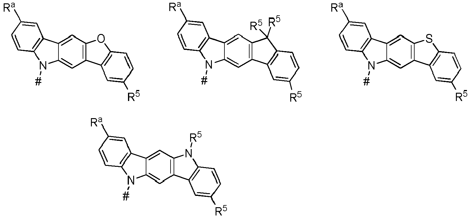


- In one embodiment, Ra and R5 is at each occurrence independently from another selected from the group consisting of hydrogen (H), methyl (Me), i-propyl (CH(CH3)2) (iPr), t-butyl (tBu), phenyl (Ph), CN, CF3, and diphenylamine (NPh2).
- In one embodiment of the invention, the organic molecules comprise or consist of a structure of formula III:

- In a further embodiment of the invention, the organic molecules comprise or consist of a structure of formula IIIa-I or formula IIIa-II:

- Rc is at each occurrence independently from another selected from the group consisting of: Me,
- iPr,
- tBu,
- Ph, which is optionally substituted with one or more substituents independently from each other selected from the group consisting of Me, iPr, tBu, CN, CF3, and Ph,
- pyridinyl, which is optionally substituted with one or more substituents independently from each other selected from the group consisting of Me, iPr, tBu, CN, CF3, and Ph,
- pyrimidinyl, which is optionally substituted with one or more substituents independently from
- each other selected from the group consisting of Me, iPr, tBu, CN, CF3, and Ph, carbazolyl, which is optionally substituted with one or more substituents independently from
- each other selected from the group consisting of Me, iPr, tBu, CN, CF3, and Ph, triazinyl, which is optionally substituted with one or more substituents independently from each
- other selected from the group consisting of Me, iPr, tBu, CN, CF3, and Ph, and
- N(Ph)2,
- and wherein R11, R12, R13, R14, R15 and RI are defined as above.
- In further embodiments of the invention, the organic molecule comprises or consists of a structure of formula IIIb-I or formula IIIb-II:
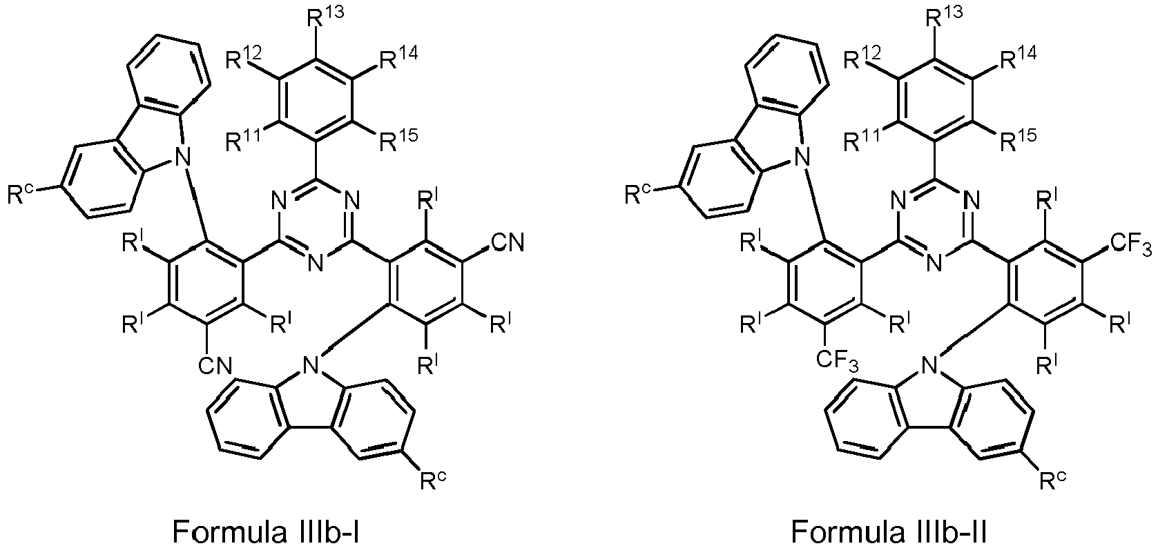
- In further embodiments of the invention, the organic molecules comprise or consist of a structure of formula IIIc-I or formula IIIc-II:

- In further embodiments of the invention, the organic molecules comprise or consist of a structure of formula IIId-I or formula IIId-II:
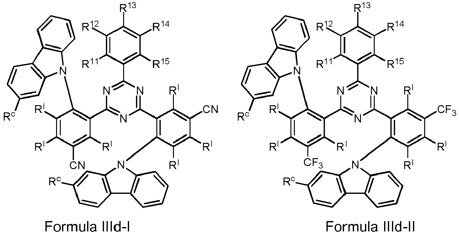
- In further embodiments of the invention, the organic molecules comprise or consist of a structure of formula IIIe-I or formula IIIeII:

- In further embodiments of the invention, the organic molecules comprise or consist of a structure of formula IIIf-I or formula IIIf-II:

- In further embodiments of the invention, the organic molecules comprise or consist of a structure of formula IIIg-I or formula IIIg-II:

- In further embodiments of the invention, the organic molecules comprise or consist of a structure of formula IIIh-I or formula IIIh-II:
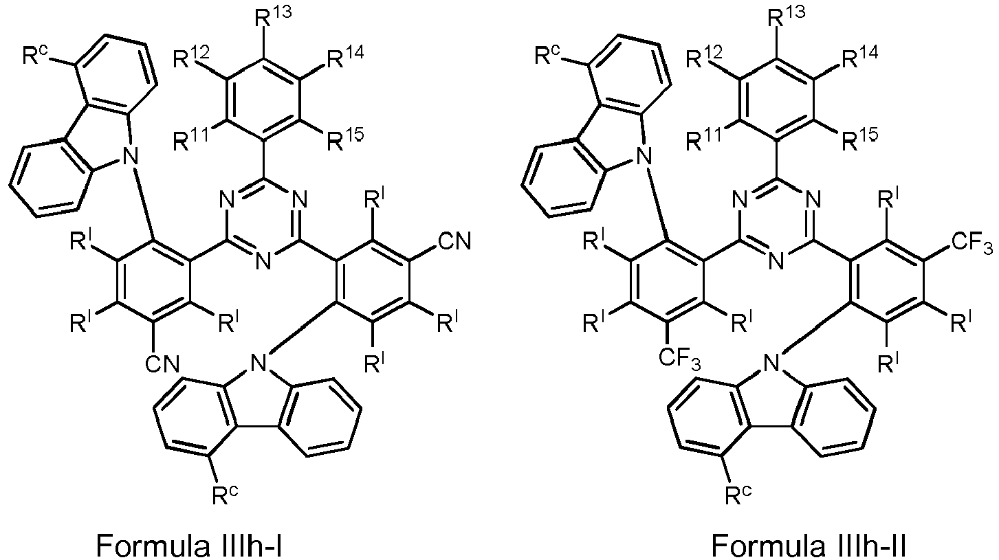
- As used above and herein, the terms "aryl" and "aromatic" may be understood in the broadest sense as any mono-, bi- or polycyclic aromatic moieties. Accordingly, an aryl group contains 6 to 60 aromatic ring atoms, and a heteroaryl group contains 5 to 60 aromatic ring atoms, of which at least one is a heteroatom. Notwithstanding, throughout the application the number of aromatic ring atoms may be given as subscripted number in the definition of certain substituents. In particular, the heteroaromatic ring includes one to three heteroatoms. Again, the terms "heteroaryl" and "heteroaromatic" may be understood in the broadest sense as any mono-, bi- or polycyclic hetero-aromatic moieties that include at least one heteroatom. The heteroatoms may at each occurrence be the same or different and be individually selected from the group consisting of N, O and S. Accordingly, the term "arylene" refers to a divalent substituent that bears two binding sites to other molecular structures and thereby serving as a linker structure. In case, a group in the exemplary embodiments is defined differently from the definitions given here, for example, the number of aromatic ring atoms or number of heteroatoms differs from the given definition, the definition in the exemplary embodiments is to be applied. According to the invention, a condensed (annulated) aromatic or heteroaromatic polycycle is built of two or more single aromatic or heteroaromatic cycles, which formed the polycycle via a condensation reaction.
- In particular, as used throughout the present application the term aryl group or heteroaryl group comprises groups which can be bound via any position of the aromatic or heteroaromatic group, derived from benzene, naphthaline, anthracene, phenanthrene, pyrene, dihydropyrene, chrysene, perylene, fluoranthene, benzanthracene, benzphenanthrene, tetracene, pentacene, benzpyrene, furan, benzofuran, isobenzofuran, dibenzofuran, thiophene, benzothiophene, isobenzothiophene, dibenzothiophene; pyrrole, indole, isoindole, carbazole, pyridine, quinoline, isoquinoline, acridine, phenanthridine, benzo-5,6-quinoline, benzo-6,7-quinoline, benzo-7,8-quinoline, phenothiazine, phenoxazine, pyrazole, indazole, imidazole, benzimidazole, naphthoimidazole, phenanthroimidazole, pyridoimidazole, pyrazinoimidazole, quinoxalinoimidazole, oxazole, benzoxazole, napthooxazole, anthroxazol, phenanthroxazol, isoxazole, 1,2-thiazole, 1,3-thiazole, benzothiazole, pyridazine, benzopyridazine, pyrimidine, benzopyrimidine, 1,3,5-triazine, quinoxaline, pyrazine, phenazine, naphthyridine, carboline, benzocarboline, phenanthroline, 1,2,3-triazole, 1,2,4-triazole, benzotriazole, 1,2,3-oxadiazole, 1,2,4-oxadiazole, 1,2,5-oxadiazole, 1,2,3,4-tetrazine, purine, pteridine, indolizine and benzothiadiazole or combinations of the abovementioned groups.
- As used throughout the present application the term cyclic group may be understood in the broadest sense as any mono-, bi- or polycyclic moieties.
- As used above and herein, the term alkyl group may be understood in the broadest sense as any linear, branched, or cyclic alkyl substituent. In particular, the term alkyl comprises the substituents methyl (Me), ethyl (Et), n-propyl (nPr), i-propyl (iPr), cyclopropyl, n-butyl (nBu), i-butyl (iBu), s-butyl (sBu), t-butyl (tBu), cyclobutyl, 2-methylbutyl, n-pentyl, s-pentyl, t-pentyl, 2-pentyl, neo-pentyl, cyclopentyl, n-hexyl, s-hexyl, t-hexyl, 2-hexyl, 3-hexyl, neo-hexyl, cyclohexyl, 1-methylcyclopentyl, 2-methylpentyl, n-heptyl, 2-heptyl, 3-heptyl, 4-heptyl, cycloheptyl, 1-methylcyclohexyl, n-octyl, 2-ethylhexyl, cyclooctyl, 1-bicyclo[2,2,2]octyl, 2-bicyclo[2,2,2]-octyl, 2-(2,6-dimethyl)octyl, 3-(3,7-dimethyl)octyl, adamantyl, 2,2,2-trifluorethyl, 1,1-dimethyl-n-hex-1-yl, 1,1-dimethyl-n-hept-1-yl, 1,1-dimethyl-n-oct-1-yl, 1,1-dimethyl-n-dec-1-yl, 1,1-dimethyl-n-dodec-1-yl, 1,1-dimethyl-n-tetradec-1-yl, 1,1-dimethyl-n-hexadec-1-yl, 1,1-dimethyl-n-octadec-1-yl, 1,1-diethyl-n-hex-1-yl, 1,1-diethyl-n-hept-1-yl, 1,1-diethyl-n-oct-1-yl, 1,1-diethyl-n-dec-1-yl, 1,1-diethyl-n-dodec-1-yl, 1,1-diethyl-n-tetradec-1-yl, 1,1-diethyln-n-hexadec-1-yl, 1,1-diethyl-n-octadec-1-yl, 1-(n-propyl)-cyclohex-1-yl, 1-(n-butyl)-cyclohex-1-yl, 1-(n-hexyl)-cyclohex-1-yl, 1-(n-octyl)-cyclohex-1-yl and 1-(n-decyl)-cyclohex-1-yl.
- As used above and herein, the term alkenyl comprises linear, branched, and cyclic alkenyl substituents. The term alkenyl group exemplarily comprises the substituents ethenyl, propenyl, butenyl, pentenyl, cyclopentenyl, hexenyl, cyclohexenyl, heptenyl, cycloheptenyl, octenyl, cyclooctenyl or cyclooctadienyl.
- As used above and herein, the term alkynyl comprises linear, branched, and cyclic alkynyl substituents. The term alkynyl group exemplarily comprises ethynyl, propynyl, butynyl, pentynyl, hexynyl, heptynyl or octynyl.
- As used above and herein, the term alkoxy comprises linear, branched, and cyclic alkoxy substituents. The term alkoxy group exemplarily comprises methoxy, ethoxy, n-propoxy, i-propoxy, n-butoxy, i-butoxy, s-butoxy, t-butoxy and 2-methylbutoxy.
- As used above and herein, the term thioalkoxy comprises linear, branched, and cyclic thioalkoxy substituents, in which the O of the exemplarily alkoxy groups is replaced by S.
- As used above and herein, the terms "halogen" and "halo" may be understood in the broadest sense as being preferably fluorine, chlorine, bromine or iodine.
- Whenever hydrogen (H) is mentioned herein, it could also be replaced by deuterium at each occurrence.
- It is understood that when a molecular fragment is described as being a substituent or otherwise attached to another moiety, its name may be written as if it were a fragment (e.g. naphtyl, dibenzofuryl) or as if it were the whole molecule (e.g. naphthalene, dibenzofuran). As used herein, these different ways of designating a substituent or attached fragment are considered to be equivalent.
- In one embodiment, the organic molecules according to the invention have an excited state lifetime of not more than 150 µs, of not more than 100 µs, in particular of not more than 50 µs, more preferably of not more than 10 µs or not more than 7 µs in a film of poly(methyl methacrylate) (PMMA) with 10% by weight of organic molecule at room temperature.
- In one embodiment of the invention, the organic molecules according to the invention represent thermally-activated delayed fluorescence (TADF) emitters, which exhibit a ΔEST value, which corresponds to the energy difference between the first excited singlet state (S1) and the first excited triplet state (T1), of less than 5000 cm-1, preferably less than 3000 cm-1, more preferably less than 1500 cm-1, even more preferably less than 1000 cm-1 or even less than 500 cm-1.
- In a further embodiment of the invention, the organic molecules according to the invention have an emission peak in the visible or nearest ultraviolet range, i.e., in the range of a wavelength of from 380 to 800 nm, with a full width at half maximum of less than 0.50 eV, preferably less than 0.48 eV, more preferably less than 0.45 eV, even more preferably less than 0.43 eV or even less than 0.40 eV in a film of poly(methyl methacrylate) (PMMA) with 10% by weight of organic molecule at room temperature.
- In a further embodiment of the invention, the organic molecules according to the invention have an emission peak in the visible or nearest ultraviolet range, i.e., in the range of a wavelength of from 380 to 800 nm, with a full width at half maximum of less than 0.40 eV in a film of poly(methyl methacrylate) (PMMA) with 10% by weight of organic molecule at room temperature.
- In a further embodiment of the invention, the organic molecules according to the invention have a "blue material index" (BMI), calculated by dividing the photoluminescence quantum yield (PLQY) in % by the CIEy color coordinate of the emitted light, of more than 150, in particular more than 200, preferably more than 250, more preferably of more than 300 or even more than 500.
- Orbital and excited state energies can be determined either by means of experimental methods or by calculations employing quantum-chemical methods, in particular density functional theory calculations. The energy of the highest occupied molecular orbital EHOMO is determined by methods known to the person skilled in the art from cyclic voltammetry measurements with an accuracy of 0.1 eV. The energy of the lowest unoccupied molecular orbital ELUMO is determined as the onset of the absorption spectrum.
- The onset of an absorption spectrum is determined by computing the intersection of the tangent to the absorption spectrum with the x-axis. The tangent to the absorption spectrum is set at the low-energy side of the absorption band and at the point at half maximum of the maximum intensity of the absorption spectrum.
- The energy of the first excited triplet state T1 is determined from the onset of the emission spectrum at low temperature, typically at 77 K. For host compounds, where the first excited singlet state and the lowest triplet state are energetically separated by > 0.4 eV, the phosphorescence is usually visible in a steady-state spectrum in 2-Me-THF. The triplet energy can thus be determined as the onset of the phosphorescence spectrum. For TADF emitter molecules, the energy of the first excited triplet state T1 is determined from the onset of the delayed emission spectrum at 77 K, if not otherwise stated measured in a film of PMMA with 10% by weight of emitter. Both for host and emitter compounds, the energy of the first excited singlet state S1 is determined from the onset of the emission spectrum, if not otherwise stated measured in a film of PMMA with 10% by weight of host or emitter compound.
- The onset of an emission spectrum is determined by computing the intersection of the tangent to the emission spectrum with the x-axis. The tangent to the emission spectrum is set at the high-energy side of the emission band and at the point at half maximum of the maximum intensity of the emission spectrum.
- A further aspect of the invention relates to a process for preparing the organic molecules (with an optional subsequent reaction) of the invention, wherein a R11-R15-substituted 2,4-dichloro-6-phenyltriazine is used as reactant:

- For the reaction of a nitrogen heterocycle in a nucleophilic aromatic substitution with an aryl halide, preferably an aryl fluoride, typical conditions include the use of a base, such as tribasic potassium phosphate for example, in an aprotic polar solvent, such as dimethyl sulfoxide (DMSO) or N,N-dimethylformamide (DMF), for example.
- A further aspect of the invention relates to the use of an organic molecule according to the invention as a luminescent emitter or as an absorber, and/or as host material and/or as electron transport material, and/or as hole injection material, and/or as hole blocking material in an optoelectronic device.
- The optoelectronic device may be understood in the broadest sense as any device based on organic materials that is suitable for emitting light in the visible or nearest ultraviolet (UV) range, i.e., in the range of a wavelength of from 380 to 800 nm. More preferably, the optoelectronic device may be able to emit light in the visible range, i.e., of from 400 to 800 nm.
- In the context of such use, the optoelectronic device is more particularly selected from the group consisting of:
- organic light-emitting diodes (OLEDs),
- light-emitting electrochemical cells,
- OLED sensors, especially in gas and vapor sensors not hermetically externally shielded,
- organic diodes,
- organic solar cells,
- organic transistors,
- organic field-effect transistors,
- organic lasers and
- down-conversion elements.
- A light-emitting electrochemical cell consists of three layers, namely a cathode, an anode, and an active layer, which contains the organic molecule according to the invention.
- In a preferred embodiment in the context of such use, the optoelectronic device is a device selected from the group consisting of an organic light emitting diode (OLED), a light emitting electrochemical cell (LEC), an organic laser, and a light-emitting transistor.
- In one embodiment, the light-emitting layer of an organic light-emitting diode comprises not only the organic molecules according to the invention but also a host material whose triplet (T1) and singlet (S1) energy levels are energetically higher than the triplet (T1) and singlet (S1) energy levels of the organic molecule.
- A further aspect of the invention relates to a composition comprising or consisting of:
- (a) the organic molecule of the invention, in particular in the form of an emitter and/or a host, and
- (b) one or more emitter and/or host materials, which differ from the organic molecule of the invention, and
- (c) optionally, one or more dyes and/or one or more solvents.
- In a further embodiment of the invention, the composition has a photoluminescence quantum yield (PLQY) of more than 26 %, preferably more than 40 %, more preferably more than 60 %, even more preferably more than 80 % or even more than 90 % at room temperature.
- One embodiment of the invention relates to a composition comprising or consisting of:
- (i) 1-50 % by weight, preferably 5-40 % by weight, in particular 10-30 % by weight, of the organic molecule according to the invention;
- (ii) 5-98 % by weight, preferably 30-93.9 % by weight, in particular 40-88% by weight, of one host compound H;
- (iii) 1-30 % by weight, in particular 1-20 % by weight, preferably 1-5 % by weight, of at least one further emitter molecule F with a structure differing from the structure of the molecules according to the invention; and
- (iv) optionally 0-94 % by weight, preferably 0.1-65 % by weight, in particular 1-50 % by weight, of at least one further host compound D with a structure differing from the structure of the molecules according to the invention; and
- (v) optionally 0-94 % by weight, preferably 0-65 % by weight, in particular 0-50 % by weight, of a solvent.
- The components or the compositions are chosen such that the sum of the weight of the components add up to 100 %.
- In a further embodiment of the invention, the composition has an emission peak in the visible or nearest ultraviolet range, i.e., in the range of a wavelength of from 380 to 800 nm.
- In one embodiment of the invention, the at least one further emitter molecule F is a purely organic emitter.
- In one embodiment of the invention, the at least one further emitter molecule F is a purely organic TADF emitter. Purely organic TADF emitters are known from the state of the art, e.g. Wong and Zysman-Colman ("Purely Organic Thermally Activated Delayed Fluorescence Materials for Organic Light-Emitting Diodes.", Adv. Mater. 2017 Jun;29(22)).
- In one embodiment of the invention, the at least one further emitter molecule F is a fluorescence emitter, in particular a blue, a green or a red fluorescence emitter.
- In a further embodiment of the invention, the composition, containing the at least one further emitter molecule F shows an emission peak in the visible or nearest ultraviolet range, i.e., in the range of a wavelength of from 380 to 800 nm, with a full width at half maximum of less than 0.30 eV, in particular less than 0.25 eV, preferably less than 0.22 eV, more preferably less than 0.19 eV or even less than 0.17 eV at room temperature, with a lower limit of 0.05 eV.
- In one embodiment of the invention, the at least one further emitter molecule F is a fluorescence emitter, in particular a blue fluorescence emitter.
- In one embodiment, the at least one further emitter molecule F is a blue fluorescence emitter selected from the following group:


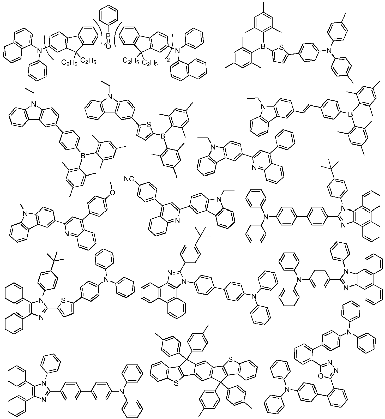

- In certain embodiments, the one further emitter molecule F is a blue fluorescence emitter selected from the following group:

- In one embodiment of the invention, the at least one further emitter molecule F is a triplet-triplet annihilation (TTA) emitter. In one embodiment, F is a blue TTA emitter selected from the following group:


- In a further embodiment of the invention, the at least one further emitter molecule F is a fluorescence emitter, in particular a green fluorescence emitter.
- In one embodiment, the at least one further emitter molecule F is a fluorescence emitter selected from the following group:


- In a further embodiment of the invention, the composition has an emission peak in the visible or nearest ultraviolet range, i.e., in the range of a wavelength of from 380 to 800 nm, in particular between 485 nm and 590 nm, preferably between 505 nm and 565 nm, even more preferably between 515 nm and 545 nm.
- In a further embodiment of the invention, the at least one further emitter molecule F is a fluorescence emitter, in particular a red fluorescence emitter.
- In one embodiment, the at least one further emitter molecule F is a fluorescence emitter selected from the following group:


- In a further embodiment of the invention, the composition has an emission peak in the visible or nearest ultraviolet range, i.e., in the range of a wavelength of from 380 to 800 nm, in particular between 590 nm and 690 nm, preferably between 610 nm and 665 nm, even more preferably between 620 nm and 640 nm.
- In one embodiment, the light-emitting layer EML of an organic light-emitting diode of the invention comprises (or essentially consists of) a composition comprising or consisting of:
- (i) 1-50 % by weight, preferably 5-40 % by weight, in particular 10-30 % by weight, of one or more organic molecules according to the invention;
- (ii) 5-99 % by weight, preferably 30-94.9 % by weight, in particular 40-89% by weight, of at least one host compound H; and
- (iii) optionally 0-94 % by weight, preferably 0.1-65 % by weight, in particular 1-50 % by weight, of at least one further host compound D with a structure differing from the structure of the molecules according to the invention; and
- (iv) optionally 0-94 % by weight, preferably 0-65 % by weight, in particular 0-50 % by weight, of a solvent; and
- (v) optionally 0-30 % by weight, in particular 0-20 % by weight, preferably 0-5 % by weight, of at least one further emitter molecule F with a structure differing from the structure of the molecules according to the invention.
- Preferably, energy can be transferred from the host compound H to the one or more organic molecules of the invention, in particular transferred from the first excited triplet state T1 (H) of the host compound H to the first excited triplet state T1 (E) of the one or more organic molecules according to the invention and/ or from the first excited singlet state S1(H) of the host compound H to the first excited singlet state S1(E) of the one or more organic molecules according to the invention.
- In one embodiment, the host compound H has a highest occupied molecular orbital HOMO(H) having an energy EHOMO(H) in the range of from -5 eV to -6.5 eV and one organic molecule according to the invention E has a highest occupied molecular orbital HOMO(E) having an energy EHOMO(E), wherein EHOMO(H) > EHOMO(E).
- In a further embodiment, the host compound H has a lowest unoccupied molecular orbital LUMO(H) having an energy ELUMO(H) and the one organic molecule according to the invention E has a lowest unoccupied molecular orbital LUMO(E) having an energy ELUMO(E), wherein ELUMO(H) > ELUMO(E).
- In a further embodiment, the light-emitting layer EML of an organic light-emitting diode of the invention comprises (or essentially consists of) a composition comprising or consisting of:
- (i) 1-50 % by weight, preferably 5-40 % by weight, in particular 10-30 % by weight, of one organic molecule according to the invention;
- (ii) 5-99 % by weight, preferably 30-94.9 % by weight, in particular 40-89% by weight, of one host compound H; and
- (iii) 0-94 % by weight, preferably 0.1-65 % by weight, in particular 1-50 % by weight, of at least one further host compound D with a structure differing from the structure of the molecules according to the invention; and
- (iv) optionally 0-94 % by weight, preferably 0-65 % by weight, in particular 0-50 % by weight, of a solvent; and
- (v) optionally 0-30 % by weight, in particular 0-20 % by weight, preferably 0-5 % by weight, of at least one further emitter molecule F with a structure differing from the structure of the molecules according to the invention.
- In one embodiment of the organic light-emitting diode of the invention, the host compound H has a highest occupied molecular orbital HOMO(H) having an energy EHOMO(H) in the range of from -5 eV to -6.5 eV and the at least one further host compound D has a highest occupied molecular orbital HOMO(D) having an energy EHOMO(D), wherein EHOMO(H) > EHOMO(D). The relation EHOMO(H) > EHOMO(D) favors an efficient hole transport.
- In a further embodiment, the host compound H has a lowest unoccupied molecular orbital LUMO(H) having an energy ELUMO(H) and the at least one further host compound D has a lowest unoccupied molecular orbital LUMO(D) having an energy ELUMO(D), wherein ELUMO(H) > ELUMO(D). The relation ELUMO(H) > ELUMO(D) favors an efficient electron transport.
- In one embodiment of the organic light-emitting diode of the invention, the host compound H has a highest occupied molecular orbital HOMO(H) having an energy EHOMO(H) and a lowest unoccupied molecular orbital LUMO(H) having an energy ELUMO(H), and
- the at least one further host compound D has a highest occupied molecular orbital HOMO(D) having an energy EHOMO(D) and a lowest unoccupied molecular orbital LUMO(D) having an energy ELUMO(D),
- the organic molecule E of the invention has a highest occupied molecular orbital HOMO(E) having an energy EHOMO(E) and a lowest unoccupied molecular orbital LUMO(E) having an energy ELUMO(E),
- In a further embodiment, the light-emitting layer EML comprises (or (essentially) consists of) a composition comprising or consisting of:
- (i) 1-50 % by weight, preferably 5-40 % by weight, in particular 10-30 % by weight, of one organic molecule according to the invention;
- (ii) 5-98 % by weight, preferably 30-93.9 % by weight, in particular 40-88% by weight, of one host compound H;
- (iii) 1-30 % by weight, in particular 1-20 % by weight, preferably 1-5 % by weight, of at least one further emitter molecule F with a structure differing from the structure of the molecules according to the invention; and
- (iv) optionally 0-94 % by weight, preferably 0.1-65 % by weight, in particular 1-50 % by weight, of at least one further host compound D with a structure differing from the structure of the molecules according to the invention; and
- (v) optionally 0-94 % by weight, preferably 0-65 % by weight, in particular 0-50 % by weight, of a solvent.
- In a further embodiment, the light-emitting layer EML comprises (or (essentially) consists of) a composition as described in Compositions with at least one further emitter, with the at least one further emitter molecule F as defined in Composition wherein the at least one further emitter molecule F is a blue fluorescence emitter.
- In a further embodiment, the light-emitting layer EML comprises (or (essentially) consists of) a composition as described in Compositions with at least one further emitter, with the at least one further emitter molecule F as defined in Composition wherein the at least one further emitter molecule F is a triplet-triplet annihilation (TTA) fluorescence emitter.
- In a further embodiment, the light-emitting layer EML comprises (or (essentially) consists of) a composition as described in Compositions with at least one further emitter, with the at least one further emitter molecule F as defined in Composition wherein the at least one further emitter molecule F is a green fluorescence emitter.
- In a further embodiment, the light-emitting layer EML comprises (or (essentially) consists of) a composition as described in Compositions with at least one further emitter, with the at least one further emitter molecule F as defined in Composition wherein the at least one further emitter molecule F is a red fluorescence emitter.
- In one embodiment of the light-emitting layer EML comprising at least one further emitter molecule F, energy can be transferred from the one or more organic molecules of the invention E to the at least one further emitter molecule F, in particular transferred from the first excited singlet state S1(E) of one or more organic molecules of the invention E to the first excited singlet state S1(F) of the at least one further emitter molecule F.
- In one embodiment, the first excited singlet state S1(H) of one host compound H of the light-emitting layer is higher in energy than the first excited singlet state S1(E) of the one or more organic molecules of the invention E: S1(H) > S1(E), and the first excited singlet state S1(H) of one host compound H is higher in energy than the first excited singlet state S1(F) of the at least one emitter molecule F: S1(H) > S1(F).
- In one embodiment, the first excited triplet state T1(H) of one host compound H is higher in energy than the first excited triplet state T1(E) of the one or more organic molecules of the invention E: T1(H) > T1(E), and the first excited triplet state T1(H) of one host compound H is higher in energy than the first excited triplet state T1(F) of the at least one emitter molecule F: T1(H) > T1(F).
- In one embodiment, the first excited singlet state S1(E) of the one or more organic molecules of the invention E is higher in energy than the first excited singlet state S1(F) of the at least one emitter molecule F: S1(E) > S1(F).
- In one embodiment, the first excited triplet state T1(E) of the one or more organic molecules E of the invention is higher in energy than the first excited singlet state T1(F) of the at least one emitter molecule F: T1(E) > T1(F).
- In one embodiment, the first excited triplet state T1(E) of the one or more organic molecules E of the invention is higher in energy than the first excited singlet state T1(F) of the at least one emitter molecule F: T1 (E) > T1(F), wherein the absolute value of the energy difference between T1(E) and T1(F) is larger than 0.3 eV, preferably larger than 0.4 eV, or even larger than 0.5 eV.
- In one embodiment, the host compound H has a highest occupied molecular orbital HOMO(H) having an energy EHOMO(H) and a lowest unoccupied molecular orbital LUMO(H) having an energy ELUMO(H), and
- the one organic molecule according to the invention E has a highest occupied molecular orbital HOMO(E) having an energy EHOMO(E) and a lowest unoccupied molecular orbital LUMO(E) having an energy ELUMO(E),
- the at least one further emitter molecule F has a highest occupied molecular orbital HOMO(F) having an energy EHOMO(F) and a lowest unoccupied molecular orbital LUMO(E) having an energy ELUMO(F),
- In a further aspect, the invention relates to an optoelectronic device comprising an organic molecule or a composition as described herein, more particularly in the form of a device selected from the group consisting of organic light-emitting diode (OLED), light-emitting electrochemical cell, OLED sensor, more particularly gas and vapour sensors not hermetically externally shielded, organic diode, organic solar cell, organic transistor, organic field-effect transistor, organic laser and down-conversion element.
- In a preferred embodiment, the optoelectronic device is a device selected from the group consisting of an organic light emitting diode (OLED), a light emitting electrochemical cell (LEC), and a light-emitting transistor.
- In one embodiment of the optoelectronic device of the invention, the organic molecule according to the invention is used as emission material in a light-emitting layer EML.
- In one embodiment of the optoelectronic device of the invention, the light-emitting layer EML consists of the composition according to the invention described herein.
- When the optoelectronic device is an OLED, it may, for example, exhibit the following layer structure:
- 1. substrate
- 2. anode layer A
- 3. hole injection layer, HIL
- 4. hole transport layer, HTL
- 5. electron blocking layer, EBL
- 6. emitting layer, EML
- 7. hole blocking layer, HBL
- 8. electron transport layer, ETL
- 9. electron injection layer, EIL
- 10. cathode layer,
- Furthermore, the optoelectronic device may optionally comprise one or more protective layers protecting the device from damaging exposure to harmful species in the environment including, exemplarily moisture, vapor and/or gases.
- In one embodiment of the invention, the optoelectronic device is an OLED, which exhibits the following inverted layer structure:
- 1. substrate
- 2. cathode layer
- 3. electron injection layer, EIL
- 4. electron transport layer, ETL
- 5. hole blocking layer, HBL
- 6. emitting layer, B
- 7. electron blocking layer, EBL
- 8. hole transport layer, HTL
- 9. hole injection layer, HIL
- 10. anode layer A
- In one embodiment of the invention, the optoelectronic device is an OLED, which may exhibit stacked architecture. In this architecture, contrary to the typical arrangement, where the OLEDs are placed side by side, the individual units are stacked on top of each other. Blended light may be generated with OLEDs exhibiting a stacked architecture, in particular white light may be generated by stacking blue, green and red OLEDs. Furthermore, the OLED exhibiting a stacked architecture may optionally comprise a charge generation layer (CGL), which is typically located between two OLED subunits and typically consists of a n-doped and p-doped layer with the n-doped layer of one CGL being typically located closer to the anode layer.
- In one embodiment of the invention, the optoelectronic device is an OLED, which comprises two or more emission layers between anode and cathode. In particular, this so-called tandem OLED comprises three emission layers, wherein one emission layer emits red light, one emission layer emits green light and one emission layer emits blue light, and optionally may comprise further layers such as charge generation layers, blocking or transporting layers between the individual emission layers. In a further embodiment, the emission layers are adjacently stacked. In a further embodiment, the tandem OLED comprises a charge generation layer between each two emission layers. In addition, adjacent emission layers or emission layers separated by a charge generation layer may be merged.
- The substrate may be formed by any material or composition of materials. Most frequently, glass slides are used as substrates. Alternatively, thin metal layers (e.g., copper, gold, silver or aluminum films) or plastic films or slides may be used. This may allow a higher degree of flexibility. The anode layer A is mostly composed of materials allowing to obtain an (essentially) transparent film. As at least one of both electrodes should be (essentially) transparent in order to allow light emission from the OLED, either the anode layer A or the cathode layer C is transparent. Preferably, the anode layer A comprises a large content or even consists of transparent conductive oxides (TCOs). Such anode layer A may exemplarily comprise indium tin oxide, aluminum zinc oxide, fluorine doped tin oxide, indium zinc oxide, PbO, SnO, zirconium oxide, molybdenum oxide, vanadium oxide, wolfram oxide, graphite, doped Si, doped Ge, doped GaAs, doped polyaniline, doped polypyrrol and/or doped polythiophene.
- Preferably, the anode layer A (essentially) consists of indium tin oxide (ITO) (e.g., (InO3)0.9(SnO2)0.1). The roughness of the anode layer A caused by the transparent conductive oxides (TCOs) may be compensated by using a hole injection layer (HIL). Further, the HIL may facilitate the injection of quasi charge carriers (i.e., holes) in that the transport of the quasi charge carriers from the TCO to the hole transport layer (HTL) is facilitated. The hole injection layer (HIL) may comprise poly-3,4-ethylendioxy thiophene (PEDOT), polystyrene sulfonate (PSS), MoO2, V2O5, CuPC or Cul, in particular a mixture of PEDOT and PSS. The hole injection layer (HIL) may also prevent the diffusion of metals from the anode layer A into the hole transport layer (HTL). The HIL may exemplarily comprise PEDOT:PSS (poly-3,4-ethylendioxy thiophene: polystyrene sulfonate), PEDOT (poly-3,4-ethylendioxy thiophene), mMTDATA (4,4',4"-tris[phenyl(m-tolyl)amino]triphenylamine), Spiro-TAD (2,2',7,7'-tetrakis(n,n-diphenylamino)-9,9'-spirobifluorene), DNTPD (N1,N1'-(biphenyl-4,4'-diyl)bis(N1-phenyl-N4,N4-di-m-tolylbenzene-1,4-diamine), NPB (N,N'-nis-(1-naphthalenyl)-N,N'-bisphenyl-(1,1'-biphenyl)-4,4'-diamine), NPNPB (N,N'-diphenyl-N,N'-di-[4-(N,N-diphenyl-amino)phenyl]benzidine), MeO-TPD (N,N,N',N'-tetrakis(4-methoxyphenyl)benzidine), HAT-CN (1,4,5,8,9,11-hexaazatriphenylen-hexacarbonitrile) and/or Spiro-NPD (N,N'-diphenyl-N,N'-bis-(1-naphthyl)-9,9'-spirobifluorene-2,7-diamine).
- Adjacent to the anode layer A or hole injection layer (HIL) typically a hole transport layer (HTL) is located. Herein, any hole transport compound may be used. Exemplarily, electron-rich heteroaromatic compounds such as triarylamines and/or carbazoles may be used as hole transport compound. The HTL may decrease the energy barrier between the anode layer A and the light-emitting layer EML. The hole transport layer (HTL) may also be an electron blocking layer (EBL). Preferably, hole transport compounds bear comparably high energy levels of their triplet states T1. Exemplarily the hole transport layer (HTL) may comprise a star-shaped heterocycle such as tris(4-carbazoyl-9-ylphenyl)amine (TCTA), poly-TPD (poly(4-butylphenyl-diphenyl-amine)), [alpha]-NPD (poly(4-butylphenyl-diphenyl-amine)), TAPC (4,4'-cyclohexyliden-bis[N,N-bis(4-methylphenyl)benzenamine]), 2-TNATA (4,4',4"-tris[2-naphthyl(phenyl)amino]triphenylamine), Spiro-TAD, DNTPD, NPB, NPNPB, MeO-TPD, HAT-CN and/or TrisPcz (9,9'-diphenyl-6-(9-phenyl-9H-carbazol-3-yl)-9H,9'H-3,3'-bicarbazole). In addition, the HTL may comprise a p-doped layer, which may be composed of an inorganic or organic dopant in an organic hole-transporting matrix. Transition metal oxides such as vanadium oxide, molybdenum oxide or tungsten oxide may exemplarily be used as inorganic dopant. Tetrafluorotetracyanoquinodimethane (F4-TCNQ), copper-pentafluorobenzoate (Cu(I)pFBz) or transition metal complexes may exemplarily be used as organic dopant.
- The EBL may exemplarily comprise mCP (1,3-bis(carbazol-9-yl)benzene), TCTA, 2-TNATA, mCBP (3,3-di(9H-carbazol-9-yl)biphenyl), tris-Pcz, CzSi (9-(4-tert-Butylphenyl)-3,6-bis(triphenylsilyl)-9H-carbazole), and/or DCB (N,N'-dicarbazolyl-1,4-dimethylbenzene).
- Adjacent to the hole transport layer (HTL), typically, the light-emitting layer EML is located. The light-emitting layer EML comprises at least one light emitting molecule. Particular, the EML comprises at least one light emitting molecule according to the invention. Typically, the EML additionally comprises one or more host material. Exemplarily, the host material is selected from CBP (4,4'-Bis-(N-carbazolyl)-biphenyl), mCP, mCBP Sif87 (dibenzo[b,d]thiophen-2-yltriphenylsilane), CzSi, Sif88 (dibenzo[b,d]thiophen-2-yl)diphenylsilane), DPEPO (bis[2-(diphenylphosphino)phenyl] ether oxide), 9-[3-(dibenzofuran-2-yl)phenyl]-9H-carbazole, 9-[3-(dibenzofuran-2-yl)phenyl]-9H-carbazole, 9-[3-(dibenzothiophen-2-yl)phenyl]-9H-carbazole, 9-[3,5-bis(2-dibenzofuranyl)phenyl]-9H-carbazole, 9-[3,5-bis(2-dibenzothiophenyl)phenyl]-9H-carbazole, T2T (2,4,6-tris(biphenyl-3-yl)-1,3,5-triazine), T3T (2,4,6-tris(triphenyl-3-yl)-1,3,5-triazine) and/or TST (2,4,6-tris(9,9'-spirobifluorene-2-yl)-1,3,5-triazine). The host material typically should be selected to exhibit first triplet (T1) and first singlet (S1) energy levels, which are energetically higher than the first triplet (T1) and first singlet (S1) energy levels of the organic molecule.
- In one embodiment of the invention, the EML comprises a so-called mixed-host system with at least one hole-dominant host and one electron-dominant host. In a particular embodiment, the EML comprises exactly one light emitting molecule species according to the invention and a mixed-host system comprising T2T as electron-dominant host and a host selected from CBP, mCP, mCBP, 9-[3-(dibenzofuran-2-yl)phenyl]-9H-carbazole, 9-[3-(dibenzofuran-2-yl)phenyl]-9H-carbazole, 9-[3-(dibenzothiophen-2-yl)phenyl]-9H-carbazole, 9-[3,5-bis(2-dibenzofuranyl)phenyl]-9H-carbazole and 9-[3,5-bis(2-dibenzothiophenyl)phenyl]-9H-carbazole as hole-dominant host. In a further embodiment the EML comprises 50-80 % by weight, preferably 60-75 % by weight of a host selected from CBP, mCP, mCBP, 9-[3-(dibenzofuran-2-yl)phenyl]-9H-carbazole, 9-[3-(dibenzofuran-2-yl)phenyl]-9H-carbazole, 9-[3-(dibenzothiophen-2-yl)phenyl]-9H-carbazole, 9-[3,5-bis(2-dibenzofuranyl)phenyl]-9H-carbazole and 9-[3,5-bis(2-dibenzothiophenyl)phenyl]-9H-carbazole; 10-45 % by weight, preferably 15-30 % by weight of T2T and 5-40 % by weight, preferably 10-30 % by weight of light emitting molecule according to the invention.
- Adjacent to the light-emitting layer EML an electron transport layer (ETL) may be located. Herein, any electron transporter may be used. Exemplarily, compounds poor of electrons such as, e.g., benzimidazoles, pyridines, triazoles, oxadiazoles (e.g., 1,3,4-oxadiazole), phosphinoxides and sulfone, may be used. An electron transporter may also be a star-shaped heterocycle such as 1,3,5-tri(1-phenyl-1H-benzo[d]imidazol-2-yl)phenyl (TPBi). The ETL may comprise NBphen (2,9-bis(naphthalen-2-yl)-4,7-diphenyl-1,10-phenanthroline), Alq3 (Aluminum-tris(8-hydroxyquinoline)), TSPO1 (diphenyl-4-triphenylsilylphenyl-phosphinoxide), BPyTP2 (2,7-di(2,2'-bipyridin-5-yl)triphenyle), Sif87 (dibenzo[b,d]thiophen-2-yltriphenylsilane), Sif88 (dibenzo[b,d]thiophen-2-yl)diphenylsilane), BmPyPhB (1,3-bis[3,5-di(pyridin-3-yl)phenyl]benzene) and/or BTB (4,4'-bis-[2-(4,6-diphenyl-1,3,5-triazinyl)]-1,1'-biphenyl). Optionally, the ETL may be doped with materials such as Liq. The electron transport layer (ETL) may also block holes or a holeblocking layer (HBL) is introduced.
- The HBL may, for example, comprise BCP (2,9-dimethyl-4,7-diphenyl-1,10-phenanthroline = Bathocuproine), BAlq (bis(8-hydroxy-2-methylquinoline)-(4-phenylphenoxy)aluminum), NBphen (2,9-bis(naphthalen-2-yl)-4,7-diphenyl-1,10-phenanthroline), Alq3 (Aluminum-tris(8-hydroxyquinoline)), TSPO1 (diphenyl-4-triphenylsilylphenyl-phosphinoxide), T2T (2,4,6-tris(biphenyl-3-yl)-1,3,5-triazine), T3T (2,4,6-tris(triphenyl-3-yl)-1,3,5-triazine), TST (2,4,6-tris(9,9'-spirobifluorene-2-yl)-1,3,5-triazine), and/or TCB/TCP (1,3,5-tris(N-carbazolyl)benzol/ 1,3,5-tris(carbazol)-9-yl) benzene).
- A cathode layer C may be located adjacent to the electron transport layer (ETL). For example, the cathode layer C may comprise or may consist of a metal (e.g., Al, Au, Ag, Pt, Cu, Zn, Ni, Fe, Pb, LiF, Ca, Ba, Mg, In, W, or Pd) or a metal alloy. For practical reasons, the cathode layer may also consist of (essentially) non-transparent metals such as Mg, Ca or Al. Alternatively or additionally, the cathode layer C may also comprise graphite and or carbon nanotubes (CNTs). Alternatively, the cathode layer C may also consist of nanoscalic silver wires.
- An OLED may further, optionally, comprise a protection layer between the electron transport layer (ETL) and the cathode layer C (which may be designated as electron injection layer (EIL)). This layer may comprise lithium fluoride, cesium fluoride, silver, Liq (8-hydroxyquinolinolatolithium), Li2O, BaF2, MgO and/or NaF.
- Optionally, also the electron transport layer (ETL) and/or a hole blocking layer (HBL) may comprise one or more host compounds.
- In order to modify the emission spectrum and/or the absorption spectrum of the light-emitting layer EML further, the light-emitting layer EML may further comprise one or more further emitter molecule F. Such an emitter molecule F may be any emitter molecule known in the art. Preferably such an emitter molecule F is a molecule with a structure differing from the structure of the molecules according to the invention. The emitter molecule F may optionally be a TADF emitter. Alternatively, the emitter molecule F may optionally be a fluorescent and/or phosphorescent emitter molecule which is able to shift the emission spectrum and/or the absorption spectrum of the light-emitting layer EML. For example, the triplet and/or singlet excitons may be transferred from the emitter molecule according to the invention to the emitter molecule F before relaxing to the ground state S0 by emitting light typically red-shifted in comparison to the light emitted by emitter molecule E. Optionally, the emitter molecule F may also provoke two-photon effects (i.e., the absorption of two photons of half the energy of the absorption maximum).
- Optionally, an optoelectronic device (e.g., an OLED) may, for example, be an essentially white optoelectronic device. Exemplarily such white optoelectronic device may comprise at least one (deep) blue emitter molecule and one or more emitter molecules emitting green and/or red light. Then, there may also optionally be energy transmittance between two or more molecules as described above.
- As used herein, if not defined more specifically in the particular context, the designation of the colors of emitted and/or absorbed light is as follows:
violet: wavelength range of >380-420 nm; deep blue: wavelength range of >420-480 nm; sky blue: wavelength range of >480-500 nm; green: wavelength range of >500-560 nm; yellow: wavelength range of >560-580 nm; orange: wavelength range of >580-620 nm; red: wavelength range of >620-800 nm. - With respect to emitter molecules, such colors refer to the emission maximum. Therefore, exemplarily, a deep blue emitter has an emission maximum in the range of from >420 to 480 nm, a sky-blue emitter has an emission maximum in the range of from >480 to 500 nm, a green emitter has an emission maximum in a range of from >500 to 560 nm, a red emitter has an emission maximum in a range of from >620 to 800 nm.
- A further embodiment of the present invention relates to an OLED, which emits light with CIEx and CIEy color coordinates close to the CIEx (= 0.131) and CIEy (= 0.046) color coordinates of the primary color blue (CIEx = 0.131 and CIEy = 0.046) as defined by ITU-R Recommendation BT.2020 (Rec. 2020) and thus is suited for the use in Ultra High Definition (UHD) displays, e.g. UHD-TVs. In this context, the term "close to" refers to the ranges of CIEx and CIEy coordinates provided at the end of this paragraph. In commercial applications, typically top-emitting (top-electrode is transparent) devices are used, whereas test devices as described throughout the present application represent bottom-emitting devices (bottom-electrode and substrate are transparent). The CIEy color coordinate of a blue device can be reduced by up to a factor of two, when changing from a bottom- to a top-emitting device, while the CIEx remains nearly unchanged (Okinaka et al. doi:10.1002/sdtp.10480). Accordingly, a further embodiment of the present invention relates to an OLED, whose emission exhibits a CIEx color coordinate of between 0.02 and 0.30, preferably between 0.03 and 0.25, more preferably between 0.05 and 0.20 or even more preferably between 0.08 and 0.18 or even between 0.10 and 0.15 and/ or a CIEy color coordinate of between 0.00 and 0.45, preferably between 0.01 and 0.30, more preferably between 0.02 and 0.20 or even more preferably between 0.03 and 0.15 or even between 0.04 and 0.10.
- A further embodiment of the present invention relates to an OLED, which emits light with CIEx and CIEy color coordinates close to the CIEx (= 0.170) and CIEy (= 0.797) color coordinates of the primary color green (CIEx = 0.170 and CIEy = 0.797) as defined by ITU-R Recommendation BT.2020 (Rec. 2020) and thus is suited for the use in Ultra High Definition (UHD) displays, e.g. UHD-TVs. In this context, the term "close to" refers to the ranges of CIEx and CIEy coordinates provided at the end of this paragraph. In commercial applications, typically top-emitting (top-electrode is transparent) devices are used, whereas test devices as used throughout the present application represent bottom-emitting devices (bottom-electrode and substrate are transparent). The CIEy color coordinate of a blue device can be reduced by up to a factor of two, when changing from a bottom- to a top-emitting device, while the CIEx remains nearly unchanged (Okinaka et al. doi:10.1002/sdtp.10480). Accordingly, a further aspect of the present invention relates to an OLED, whose emission exhibits a CIEx color coordinate of between 0.06 and 0.34, preferably between 0.07 and 0.29, more preferably between 0.09 and 0.24 or even more preferably between 0.12 and 0.22 or even between 0.14 and 0.19 and/ or a CIEy color coordinate of between 0.75 and 1.20, preferably between 0.76 and 1.05, more preferably between 0.77 and 0.95 or even more preferably between 0.78 and 0.90 or even between 0.79 and 0.85.
- A further embodiment of the present invention relates to an OLED, which emits light with CIEx and CIEy color coordinates close to the CIEx (= 0.708) and CIEy (= 0.292) color coordinates of the primary color red (CIEx = 0.708 and CIEy = 0.292) as defined by ITU-R Recommendation BT.2020 (Rec. 2020) and thus is suited for the use in Ultra High Definition (UHD) displays, e.g. UHD-TVs. In this context, the term "close to" refers to the ranges of CIEx and CIEy coordinates provided at the end of this paragraph. In commercial applications, typically top-emitting (top-electrode is transparent) devices are used, whereas test devices as used throughout the present application represent bottom-emitting devices (bottom-electrode and substrate are transparent). The CIEy color coordinate of a blue device can be reduced by up to a factor of two, when changing from a bottom- to a top-emitting device, while the CIEx remains nearly unchanged (Okinaka et al. doi:10.1002/sdtp.10480). Accordingly, a further aspect of the present invention relates to an OLED, whose emission exhibits a CIEx color coordinate of between 0.60 and 0.88, preferably between 0.61 and 0.83, more preferably between 0.63 and 0.78 or even more preferably between 0.66 and 0.76 or even between 0.68 and 0.73 and/ or a CIEy color coordinate of between 0.25 and 0.70, preferably between 0.26 and 0.55, more preferably between 0.27 and 0.45 or even more preferably between 0.28 and 0.40 or even between 0.29 and 0.35.
- Accordingly, a further aspect of the present invention relates to an OLED, which exhibits an external quantum efficiency at 1000 cd/m2 of more than 8%, more preferably of more than 10%, more preferably of more than 13%, even more preferably of more than 15% or even more than 20% and/or exhibits an emission maximum between 420 nm and 500 nm, preferably between 430 nm and 490 nm, more preferably between 440 nm and 480 nm, even more preferably between 450 nm and 470 nm and/or exhibits a LT80 value at 500 cd/m2 of more than 100 h, preferably more than 200 h, more preferably more than 400 h, even more preferably more than 750 h or even more than 1000 h.
- The optoelectronic device, in particular the OLED according to the present invention can be manufactured by any means of vapor deposition and/ or liquid processing. Accordingly, at least one layer is
- prepared by means of a sublimation process,
- prepared by means of an organic vapor phase deposition process,
- prepared by means of a carrier gas sublimation process,
- solution processed or
- printed.
- The methods used to manufacture the optoelectronic device, in particular the OLED according to the present invention are known in the art. The different layers are individually and successively deposited on a suitable substrate by means of subsequent deposition processes. The individual layers may be deposited using the same or differing deposition methods.
- Vapor deposition processes exemplarily comprise thermal (co)evaporation, chemical vapor deposition and physical vapor deposition. For active matrix OLED display, an AMOLED backplane is used as substrate. The individual layer may be processed from solutions or dispersions employing adequate solvents. Solution deposition process exemplarily comprise spin coating, dip coating and jet printing. Liquid processing may optionally be carried out in an inert atmosphere (e.g., in a nitrogen atmosphere) and the solvent may optionally be completely or partially removed by means known in the state of the art.
-

-

-
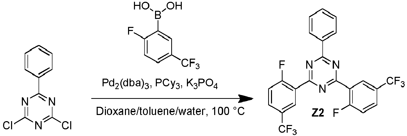
- The synthesis of Z2 is carried out according to AAV1, wherein 2,4-Dichloro-6-phenyl-1,3,5-triazine reacts with 2-fluoro-5-(trifluoromethyl)phenylboronic acid.
-


- Z1 or Z2 (1 equivalent each), the corresponding donor molecule D-H (2.20 equivalents) and tribasic potassium phosphate (4.40 equivalents) are suspended under nitrogen atmosphere in DMSO and stirred at 100-120 °C (20 h). Subsequently, the reaction mixture is poured into a saturated sodium chloride solution and the precipitate is filtered and washed with water. The solid is then dissolved in dichloromethane, dried over MgSO4 and the solvent is evaporated under reduced pressure. The crude product is purified by recrystallization or by flash chromatography. The product is obtained as a solid.
- In particular, the donor molecule D-H is a 3,6-substituted carbazole (e.g., 3,6-dimethylcarbazole, 3,6-diphenylcarbazole, 3,6-di-tert-butylcarbazole), a 2,7-substituted carbazole (e.g., 2,7-dimethylcarbazole, 2,7-diphenylcarbazole, 2,7-di-tert-butylcarbazole), a 1,8-substituted carbazole (e.g., 1,8-dimethylcarbazole, 1,8-diphenylcarbazole, 1,8-di-tert-butylcarbazole), a 1-substituted carbazole (e.g., 1-methylcarbazole, 1-phenylcarbazole, 1-tert-butylcarbazole), a 2-substituted carbazole (e.g., 2-methylcarbazole, 2-phenylcarbazole, 2-tert-butylcarbazole), or a 3-substituted carbazole (e.g., 3-methylcarbazole, 3-phenylcarbazole, 3-tert-butylcarbazole).
- Exemplarily a halogen-substituted carbazole, particularly 3-bromocarbazole, can be used as D-H.
- In a subsequent reaction a boronic acid ester functional group or boronic acid functional group may be exemplarily introduced at the position of the one or more halogen substituents, which was introduced via D-H, to yield the corresponding carbazol-3-ylboronic acid ester or carbazol-3-ylboronic acid, e.g., via the reaction with bis(pinacolato)diboron (CAS No. 73183-34-3). Subsequently, one or more substituents Ra may be introduced in place of the boronic acid ester group or the boronic acid group via a coupling reaction with the corresponding halogenated reactant Ra-Hal, preferably Ra-Cl and Ra-Br.
- Alternatively, one or more substituents Ra may be introduced at the position of the one or more halogen substituents, which was introduced via D-H, via the reaction with a boronic acid of the substituent Ra [Ra-B(OH)2] or a corresponding boronic acid ester.
- HPLC-MS spectroscopy is performed on a HPLC by Agilent (1100 series) with MS-detector (Thermo LTQ XL). A reverse phase column 4,6mm x 150mm, particle size 5,0 µm from Waters (without pre-column) is used in the HPLC. The HPLC-MS measurements are performed at room temperature (rt) with the solvents acetonitrile, water and THF in the following concentrations:
solvent A: H2O (90%) MeCN (10%) solvent B: H2O (10%) MeCN (90%) solvent C: THF (100%) - From a solution with a concentration of 0.5mg/ml an injection volume of 15 µL is taken for the measurements. The following gradient is used:
Flow rate [ml/min] time [min] A[%] B[%] D[%] 3 0 40 50 10 3 10 10 15 75 3 16 10 15 75 3 16.01 40 50 10 3 20 40 50 10 - Cyclic voltammograms are measured from solutions having concentration of 10-3 mol/l of the organic molecules in dichloromethane or a suitable solvent and a suitable supporting electrolyte (e.g. 0.1 mol/l of tetrabutylammonium hexafluorophosphate). The measurements are conducted at room temperature under nitrogen atmosphere with a three-electrode assembly (Working and counter electrodes: Pt wire, reference electrode: Pt wire) and calibrated using FeCp2/FeCp2 + as internal standard. The HOMO data was corrected using ferrocene as internal standard against a SCE (saturated calomel electrode).
- Molecular structures are optimized employing the BP86 functional and the resolution of identity approach (RI). Excitation energies are calculated using the (BP86) optimized structures employing Time-Dependent DFT (TD-DFT) methods. Orbital and excited state energies are calculated with the B3LYP functional. Def2-SVP basis sets (and a m4-grid for numerical integration are used. The Turbomole program package was used for all calculations.
- Sample pretreatment: Spin-coating
Apparatus: Spin150, SPS euro. - The sample concentration is 10 mg/ml, dissolved in a suitable solvent.
Program: 1) 3 s at 400 U/min; 20 s at 1000 U/min at 1000 Upm/s. 3) 10 s at 4000 U/min at 1000 Upm/s. After coating, the films are tried at 70 °C for 1 min. - Photoluminescence spectroscopy and TCSPC (Time-correlated single-photon counting) Steady-state emission spectroscopy is measured by a Horiba Scientific, Modell FluoroMax-4 equipped with a 150 W Xenon-Arc lamp, excitation- and emissions monochromators and a Hamamatsu R928 photomultiplier and a time-correlated single-photon counting option. Emissions and excitation spectra are corrected using standard correction fits.
- Excited state lifetimes are determined employing the same system using the TCSPC method with FM-2013 equipment and a Horiba Yvon TCSPC hub.
- Excitation sources:
- NanoLED 370 (wavelength: 371 nm, puls duration: 1,1 ns)
- NanoLED 290 (wavelength: 294 nm, puls duration: <1 ns)
- SpectraLED 310 (wavelength: 314 nm)
- SpectraLED 355 (wavelength: 355 nm).
- For photoluminescence quantum yield (PLQY) measurements an Absolute PL Quantum Yield Measurement C9920-03G system (Hamamatsu Photonics) is used. Quantum yields and CIE coordinates are determined using the software U6039-05 version 3.6.0.
- Emission maxima are given in nm, quantum yields Φ in % and CIE coordinates as x,y values. PLQY is determined using the following protocol:
- 1) Quality assurance: Anthracene in ethanol (known concentration) is used as reference
- 2) Excitation wavelength: the absorption maximum of the organic molecule is determined and the molecule is excited using this wavelength
- 3) Measurement
- Quantum yields are measured for sample of solutions or films under nitrogen atmosphere. The yield is calculated using the equation:

- OLED devices comprising organic molecules according to the invention can be produced via vacuum-deposition methods. If a layer contains more than one compound, the weight-percentage of one or more compounds is given in %. The total weight-percentage values amount to 100 %, thus if a value is not given, the fraction of this compound equals to the difference between the given values and 100 %.
- The not fully optimized OLEDs are characterized using standard methods and measuring electroluminescence spectra, the external quantum efficiency (in %) in dependency on the intensity, calculated using the light detected by the photodiode, and the current. The OLED device lifetime is extracted from the change of the luminance during operation at constant current density. The LT50 value corresponds to the time, where the measured luminance decreased to 50 % of the initial luminance, analogously LT80 corresponds to the time point, at which the measured luminance decreased to 80 % of the initial luminance, LT 95 to the time point, at which the measured luminance decreased to 95 % of the initial luminance etc.
- Accelerated lifetime measurements are performed (e.g. applying increased current densities). For example, LT80 values at 500 cd/m2 are determined using the following equation:

- The values correspond to the average of several pixels (typically two to eight), the standard deviation between these pixels is given. The figures show the data series for one OLED pixel.
-
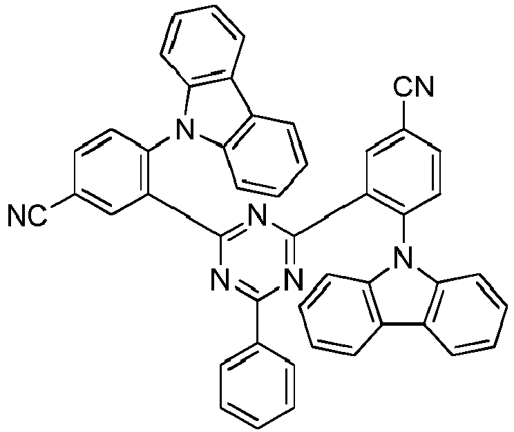
- Example 1 was synthesized according to AAV1 (yield 19%) and AAV3 (yield 22%)
-
Figure 1 depicts the emission spectrum of example 1 (10 % by weight in PMMA). The emission maximum (λmax) is at 489 nm. The photoluminescence quantum yield (PLQY) is 80 %, the full width at half maximum (FWHM) is 0.41 eV and the emission lifetime is 6 µs. The resulting CIEx coordinate is 0.22 and the CIEy coordinate is 0.44.
MS (HPLC-MS), m/z (retention time): 689.33 (8.13 min). -

- Example 2 was synthesized according to AAV2 (yield 68%) and AAV3 (yield 51%)
-
Figure 2 depicts the emission spectrum of example 2 (10 % by weight in PMMA). The emission maximum (λmax) is at 484 nm. The photoluminescence quantum yield (PLQY) is 79 %, the full width at half maximum (FWHM) is 0.43 eV and the emission lifetime is 5 µs. The resulting CIEx coordinate is 0.19 and the CIEy coordinate is 0.35.
MS (HPLC-MS), m/z (retention time): 775.35 (10.85 min). -

- Example 3 was synthesized according to AAV1 (yield 84%) and AAV3 (yield 80%)
-
Figure 3 depicts the emission spectrum of example 3 (10 % by weight in PMMA). The emission maximum (λmax) is at 519 nm. The photoluminescence quantum yield (PLQY) is 52 %, the full width at half maximum (FWHM) is 0.40 eV and the emission lifetime is 4 µs. The resulting CIEx coordinate is 0.32 and the CIEy coordinate is 0.57.
MS (HPLC-MS), m/z: 993.40. - Example 3 was tested in an OLED-device D1 with the following layer structure:
Layer Thickness 9 100 nm Al 8 2 nm Liq 7 35 nm NBphen 6 40 nm 3 (30%) : mCBP (70%) 5 5 nm mCBP 4 5 nm TCTA 3 145 nm NPB 2 5 nm HAT-CN 1 50 nm ITO Substrate Glass - For D1 an external quantum efficiency (EQE) at 1000 cd/m2 of 12.6 ± 0.1 %, a LT80-value at 500 cd/m2 of 10032 h and a LT97-value at 1200 cd/m2 of 198 h from accelerated lifetime measurements were determined. The emission maximum is at 528 nm, CIEx is 0.37 and CIEy: 0.57 at 4.5 V.
- Example 3 was tested in an OLED-device D2 with the following layer structure:
Layer Thickness 9 100 nm Al 
8 2 nm Liq 7 65 nm NBphen 6 30 nm 3 (11%): mCBP (88%): FLUO1 (1%) 5 5 nm mCBP FLUO1 4 5 nm TCTA 3 20 nm NPB 2 10 nm HAT-CN 1 50 nm ITO Substrate Glass - For D2 an external quantum efficiency (EQE) at 1000 cd/m2 of 9.6 ± 0.2 % and a LT97-value at 1200 cd/m2 of 306 h from accelerated lifetime measurements were determined. The emission maximum is at 561 nm, CIEx is 0.46 and CIEy: 0.51 at 6.4 V.
-


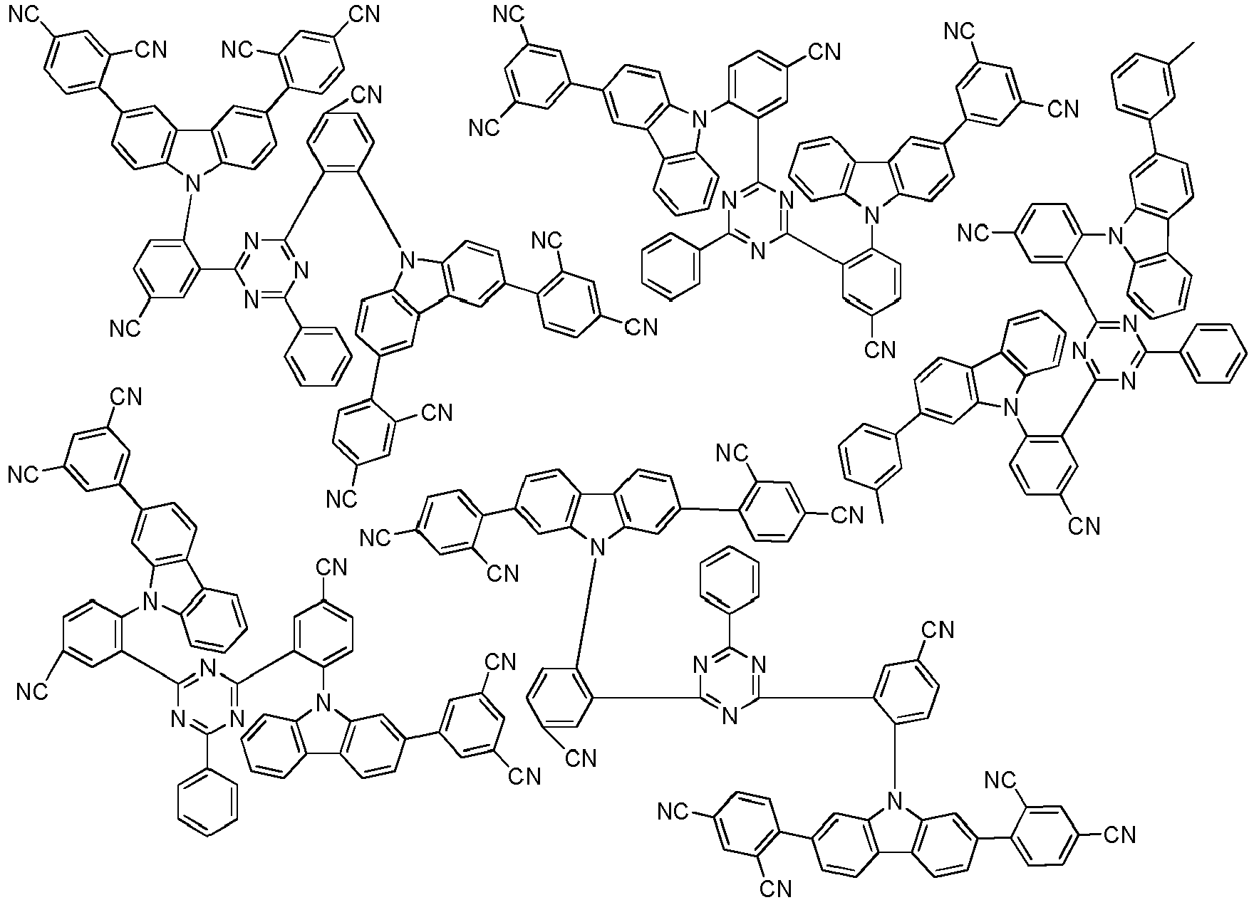


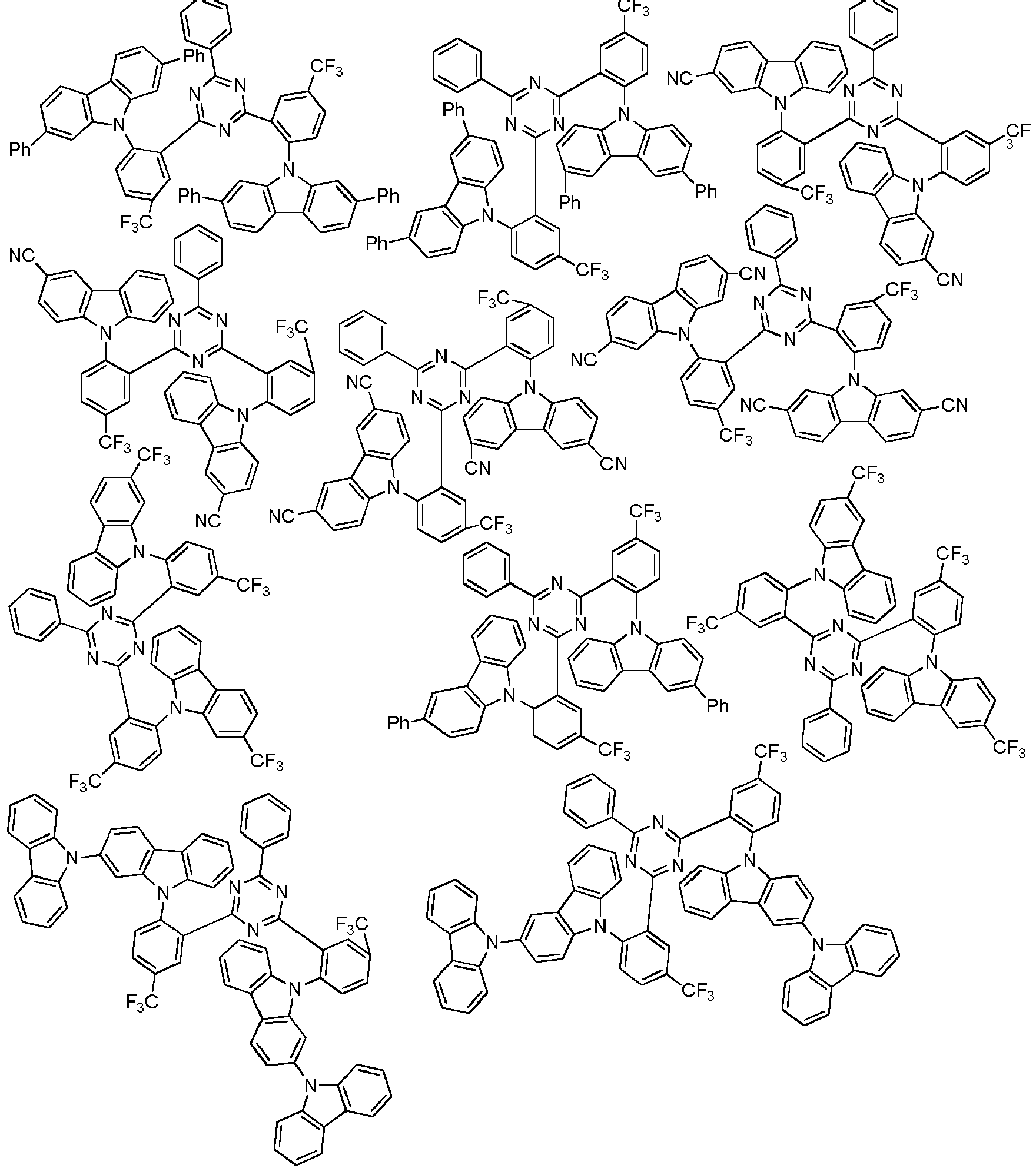


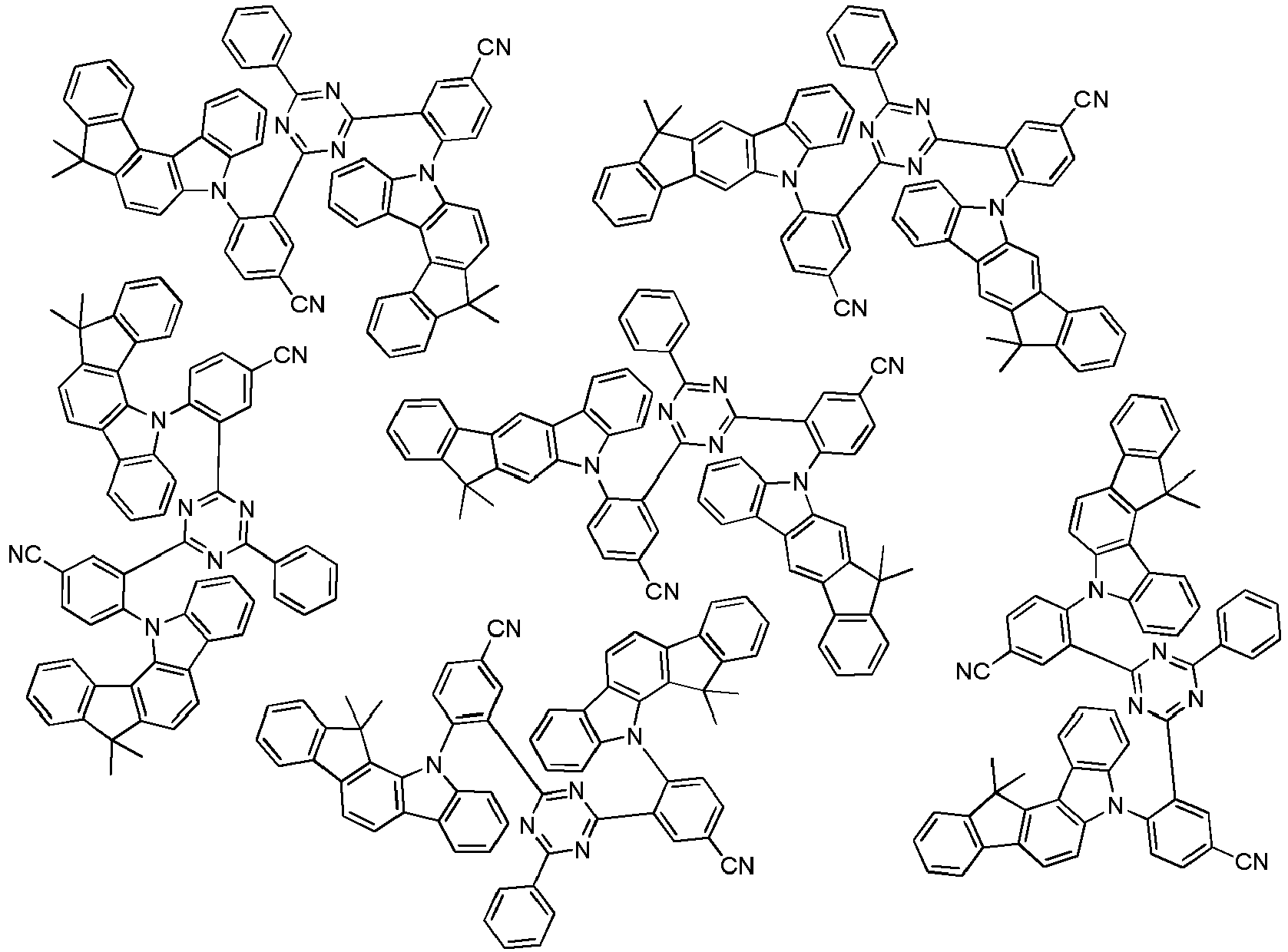


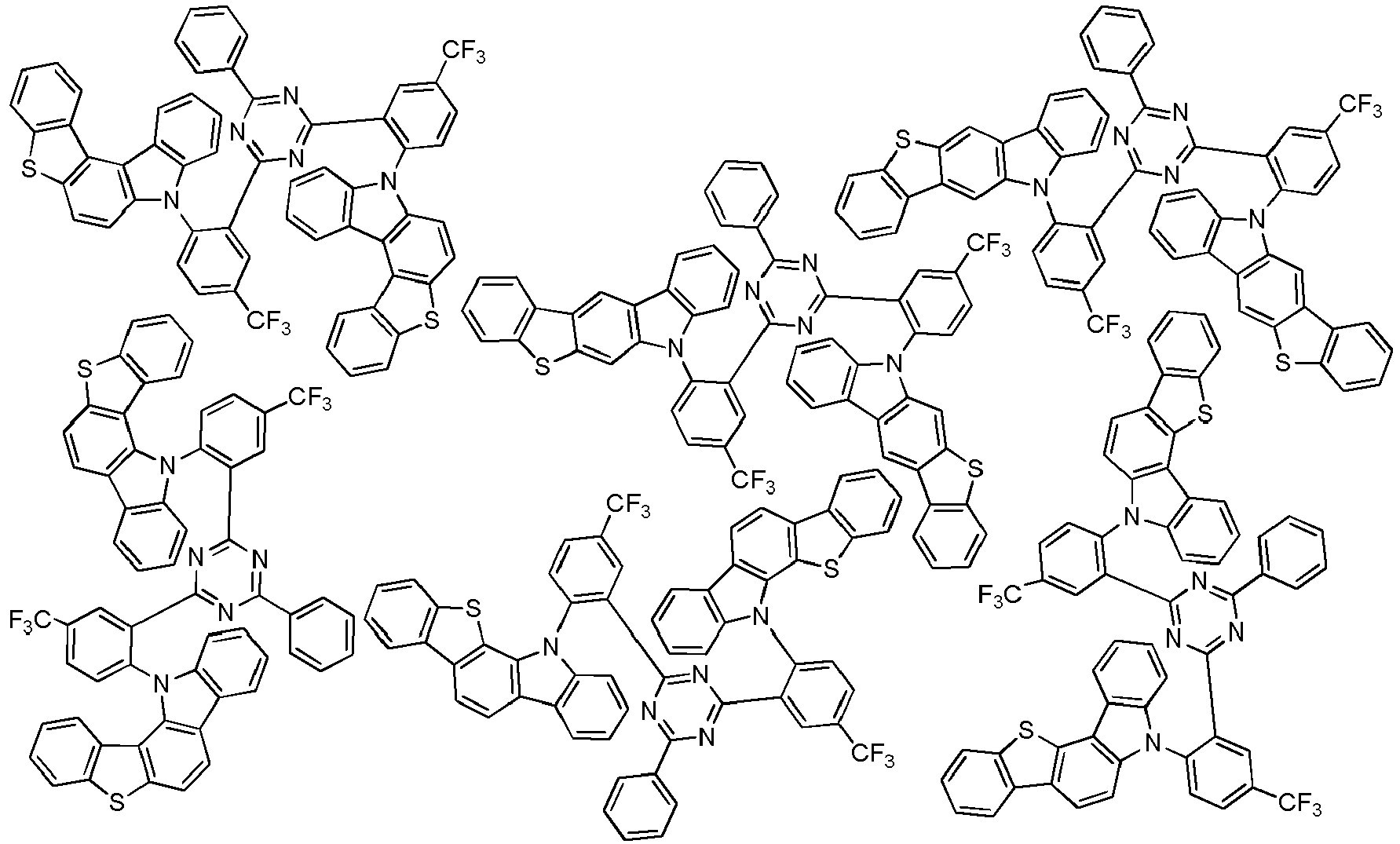

-
- Figure 1
- Emission spectrum of example 1 (10% by weight) in PMMA.
- Figure 2
- Emission spectrum of example 2 (10% by weight) in PMMA.
- Figure 3
- Emission spectrum of example 3 (10% by weight) in PMMA.
EHOMO(H) > EHOMO(D) and the difference between the energy level of the highest occupied molecular orbital HOMO(E) of organic molecule according to the invention (EHOMO(E)) and the energy level of the highest occupied molecular orbital HOMO(H) of the host compound H (EHOMO(H)) is between -0.5 eV and 0.5 eV, more preferably between -0.3 eV and 0.3 eV, even more preferably between -0.2 eV and 0.2 eV or even between -0.1 eV and 0.1 eV; and ELUMO(H) > ELUMO(D) and the difference between the energy level of the lowest unoccupied molecular orbital LUMO(E) of organic molecule according to the invention (ELUMO(E)) and the lowest unoccupied molecular orbital LUMO(D) of the at least one further host compound D (ELUMO(D)) is between -0.5 eV and 0.5 eV, more preferably between -0.3 eV and 0.3 eV, even more preferably between -0.2 eV and 0.2 eV or even between -0.1 eV and 0.1 eV.
EHOMO(H) > EHOMO(E) and the difference between the energy level of the highest occupied molecular orbital HOMO(F) of the at least one further emitter molecule (EHOMO(F)) and the energy level of the highest occupied molecular orbital HOMO(H) of the host compound H (EHOMO(H)) is between -0.5 eV and 0.5 eV, more preferably between -0.3 eV and 0.3 eV, even more preferably between -0.2 eV and 0.2 eV or even between -0.1 eV and 0.1 eV; and ELUMO(H) > ELUMO(E) and the difference between the energy level of the lowest unoccupied molecular orbital LUMO(F) of the at least one further emitter molecule (ELUMO(F)) and the lowest unoccupied molecular orbital LUMO(E) of the one organic molecule according to the invention (ELUMO(E)) is between -0.5 eV and 0.5 eV, more preferably between -0.3 eV and 0.3 eV, even more preferably between -0.2 eV and 0.2 eV or even between -0.1 eV and 0.1 eV.
Claims (15)
- Organic molecule, comprising- a first chemical moiety comprising a structure of formula I,
 - two second chemical moieties, each comprising a structure of formula II,wherein the substituents Ra, R3, R4 or R5 independently from each other optionally form a mono- or polycyclic, aliphatic, aromatic and/or benzo-fused ring system with one or more substituents Ra, R3, R4 or R5.
 wherein the first chemical moiety is linked to the second chemical moiety via a single bond;wherein# represents the binding site of the first chemical moiety to the second chemical moiety;W is the bond linking the first chemical moiety to one of the two second chemical moieties;V is selected from the group consisting of CN and CF3;Z is at each occurrence independently from another selected from the group consisting of a direct bond, CR3R4, C=CR3R4, C=O, C=NR3, NR3, O, SiR3R4, S, S(O) and S(O)2;RI is at each occurrence independently from another selected from the group consisting of: hydrogen, deuterium,C1-C5-alkyl,
wherein one or more hydrogen atoms are optionally substituted by deuterium;C2-C8-alkenyl,
wherein one or more hydrogen atoms are optionally substituted by deuterium;C2-C8-alkynyl,
wherein one or more hydrogen atoms are optionally substituted by deuterium; and C6-C18-aryl;R11, R12, R13, R14 and R15 is at each occurrence independently from another selected from the group consisting ofhydrogen, deuterium, CN, CF3, phenyl,C1-C5-alkyl,
wherein one or more hydrogen atoms are optionally substituted by deuterium;C2-C8-alkenyl,
wherein one or more hydrogen atoms are optionally substituted by deuterium;C2-C8-alkynyl,
wherein one or more hydrogen atoms are optionally substituted by deuterium; and C6-C18-aryl;Ra, R3 and R4 is at each occurrence independently from another selected from the group consisting of: hydrogen, deuterium, N(R5)2, OR5, Si(R5)3, B(OR5)2, OSO2R5, CF3, CN, F, Br, I, C1-C40-alkyl,which is optionally substituted with one or more substituents R5 andwherein one or more non-adjacent CH2-groups are optionally substituted by R5C=CR5, C≡C, Si(R5)2, Ge(R5)2, Sn(R5)2, C=O, C=S, C=Se, C=NR5, P(=O)(R5), SO, SO2, NR5, O, S or CONR5;C1-C40-alkoxy,which is optionally substituted with one or more substituents R5 andwherein one or more non-adjacent CH2-groups are optionally substituted by R5C=CR5, C≡C, Si(R5)2, Ge(R5)2, Sn(R5)2, C=O, C=S, C=Se, C=NR5, P(=O)(R5), SO, SO2, NR5, O, S or CONR5;C1-C40-thioalkoxy,which is optionally substituted with one or more substituents R5 andwherein one or more non-adjacent CH2-groups are optionally substituted by R5C=CR5, C≡C, Si(R5)2, Ge(R5)2, Sn(R5)2, C=O, C=S, C=Se, C=NR5, P(=O)(R5), SO, SO2, NR5, O, S or CONR5;C2-C40-alkenyl,which is optionally substituted with one or more substituents R5 andwherein one or more non-adjacent CH2-groups are optionally substituted by R5C=CR5, C≡C, Si(R5)2, Ge(R5)2, Sn(R5)2, C=O, C=S, C=Se, C=NR5, P(=O)(R5), SO, SO2, NR5, O, S or CONR5;C2-C40-alkynyl,which is optionally substituted with one or more substituents R5 andwherein one or more non-adjacent CH2-groups are optionally substituted by R5C=CR5, C≡C, Si(R5)2, Ge(R5)2, Sn(R5)2, C=O, C=S, C=Se, C=NR5, P(=O)(R5), SO, SO2, NR5, O, S or CONR5;C6-C60-aryl,which is optionally substituted with one or more substituents R5; and C3-C57-heteroaryl,which is optionally substituted with one or more substituents R5;R5 is at each occurrence independently from another selected from the group consisting of: hydrogen, deuterium, N(R6)2, OR6, Si(R6)3, B(OR6)2, OSO2R6, CF3, CN, F, Br, I, C1-C40-alkyl,which is optionally substituted with one or more substituents R6 andwherein one or more non-adjacent CH2-groups are optionally substituted by R6C=CR6, C≡C, Si(R6)2, Ge(R6)2, Sn(R6)2, C=O, C=S, C=Se, C=NR6, P(=O)(R6), SO, SO2, NR6, O, S or CONR6;C1-C40-alkoxy,which is optionally substituted with one or more substituents R6 andwherein one or more non-adjacent CH2-groups are optionally substituted by R6C=CR6, C≡C, Si(R6)2, Ge(R6)2, Sn(R6)2, C=O, C=S, C=Se, C=NR6, P(=O)(R6), SO, SO2, NR6, O, S or CONR6;C1-C40-thioalkoxy,which is optionally substituted with one or more substituents R6 andwherein one or more non-adjacent CH2-groups are optionally substituted by R6C=CR6, C≡C, Si(R6)2, Ge(R6)2, Sn(R6)2, C=O, C=S, C=Se, C=NR6, P(=O)(R6), SO, SO2, NR6, O, S or CONR6;C2-C40-alkenyl,which is optionally substituted with one or more substituents R6 andwherein one or more non-adjacent CH2-groups are optionally substituted by R6C=CR6, C≡C, Si(R6)2, Ge(R6)2, Sn(R6)2, C=O, C=S, C=Se, C=NR6, P(=O)(R6), SO, SO2, NR6, O, S or CONR6;C2-C40-alkynyl,which is optionally substituted with one or more substituents R6 andwherein one or more non-adjacent CH2-groups are optionally substituted by R6C=CR6, C≡C, Si(R6)2, Ge(R6)2, Sn(R6)2, C=O, C=S, C=Se, C=NR6, P(=O)(R6), SO, SO2, NR6, O, S or CONR6;C6-C60-aryl,which is optionally substituted with one or more substituents R6; and C3-C57-heteroaryl,which is optionally substituted with one or more substituents R6;R6 is at each occurrence independently from another selected from the group consisting of:hydrogen, deuterium, OPh, CF3, CN, F,C1-C5-alkyl,
wherein one or more hydrogen atoms are optionally, independently from each other substituted by deuterium, CN, CF3, or F;C1-C5-alkoxy,
wherein one or more hydrogen atoms are optionally, independently from each other substituted by deuterium, CN, CF3, or F;C1-C5-thioalkoxy,
wherein one or more hydrogen atoms are optionally, independently from each other substituted by deuterium, CN, CF3, or F;C2-C5-alkenyl,
wherein one or more hydrogen atoms are optionally, independently from each other substituted by deuterium, CN, CF3, or F;C2-C5-alkynyl,
wherein one or more hydrogen atoms are optionally, independently from each other substituted by deuterium, CN, CF3, or F;C6-C18-aryl,
which is optionally substituted with one or more C1-C5-alkyl substituents;C3-C17-heteroaryl,
which is optionally substituted with one or more C1-C5-alkyl substituents;N(C6-C18-aryl)2;N(C3-C17-heteroaryl)2, andN(C3-C17-heteroaryl)(C6-C18-aryl); - The organic molecule according to claim 1, wherein Rl, R11, R12, R13, R14, R15 is at each occurrence independently from another selected from the group consisting of H, methyl and phenyl.
- The organic molecule according to claim 1 or 2, wherein V is CN.
- The organic molecule according to one or more of claims 1 to 3, wherein the second chemical moiety comprises a structure of formula Ila:

- The organic molecule according to one or more of claims 1 to 4, wherein the second chemical moiety comprises a structure of formula IIb:
 Rb is at each occurrence independently from another selected from the group consisting of hydrogen, deuterium, N(R5)2, OR5, Si(R5)3, B(OR5)2, OSO2R5, CF3, CN, F, Br, I, C1-C40-alkyl,which is optionally substituted with one or more substituents R5 andwherein one or more non-adjacent CH2-groups are optionally substituted by R5C=CR5, C≡C, Si(R5)2, Ge(R5)2, Sn(R5)2, C=O, C=S, C=Se, C=NR5, P(=O)(R5), SO, SO2, NR5, O, S or CONR5;C1-C40-alkoxy,which is optionally substituted with one or more substituents R5 andwherein one or more non-adjacent CH2-groups are optionally substituted by R5C=CR5, C≡C, Si(R5)2, Ge(R5)2, Sn(R5)2, C=O, C=S, C=Se, C=NR5, P(=O)(R5), SO, SO2, NR5, O, S or CONR5;C1-C40-thioalkoxy,which is optionally substituted with one or more substituents R5 andwherein one or more non-adjacent CH2-groups are optionally substituted by R5C=CR5, C≡C, Si(R5)2, Ge(R5)2, Sn(R5)2, C=O, C=S, C=Se, C=NR5, P(=O)(R5), SO, SO2, NR5, O, S or CONR5;C2-C40-alkenyl,which is optionally substituted with one or more substituents R5 andwherein one or more non-adjacent CH2-groups are optionally substituted by R5C=CR5, C≡C, Si(R5)2, Ge(R5)2, Sn(R5)2, C=O, C=S, C=Se, C=NR5, P(=O)(R5), SO, SO2, NR5, O, S or CONR5;C2-C40-alkynyl,which is optionally substituted with one or more substituents R5 andwherein one or more non-adjacent CH2-groups are optionally substituted by R5C=CR5, C≡C, Si(R5)2, Ge(R5)2, Sn(R5)2, C=O, C=S, C=Se, C=NR5, P(=O)(R5), SO, SO2, NR5, O, S or CONR5;C6-C60-aryl,and wherein apart from that the definitions in claim 1 apply.which is optionally substituted with one or more substituents R5; and C3-C57-heteroaryl,which is optionally substituted with one or more substituents R5;
 - The organic molecule according to one or more of claims 1 to 4, wherein the second chemical moiety comprises a structure of formula IIc:
 Rb is at each occurrence independently from another selected from the group consisting of: hydrogen, deuterium, N(R5)2, OR5, Si(R5)3, B(OR5)2, OSO2R5, CF3, CN, F, Br, I, C1-C40-alkyl,which is optionally substituted with one or more substituents R5 andwherein one or more non-adjacent CH2-groups are optionally substituted by R5C=CR5, C≡C, Si(R5)2, Ge(R5)2, Sn(R5)2, C=O, C=S, C=Se, C=NR5, P(=O)(R5), SO, SO2, NR5, O, S or CONR5;C1-C40-alkoxy,which is optionally substituted with one or more substituents R5 andwherein one or more non-adjacent CH2-groups are optionally substituted by R5C=CR5, C≡C, Si(R5)2, Ge(R5)2, Sn(R5)2, C=O, C=S, C=Se, C=NR5, P(=O)(R5), SO, SO2, NR5, O, S or CONR5;C1-C40-thioalkoxy,which is optionally substituted with one or more substituents R5 andwherein one or more non-adjacent CH2-groups are optionally substituted by R5C=CR5, C≡C, Si(R5)2, Ge(R5)2, Sn(R5)2, C=O, C=S, C=Se, C=NR5, P(=O)(R5), SO, SO2, NR5, O, S or CONR5;C2-C40-alkenyl,which is optionally substituted with one or more substituents R5 andwherein one or more non-adjacent CH2-groups are optionally substituted by R5C=CR5, C≡C, Si(R5)2, Ge(R5)2, Sn(R5)2, C=O, C=S, C=Se, C=NR5, P(=O)(R5), SO, SO2, NR5, O, S or CONR5;C2-C40-alkynyl,which is optionally substituted with one or more substituents R5 andwherein one or more non-adjacent CH2-groups are optionally substituted by R5C=CR5, C≡C, Si(R5)2, Ge(R5)2, Sn(R5)2, C=O, C=S, C=Se, C=NR5, P(=O)(R5), SO, SO2, NR5, O, S or CONR5;C6-C60-aryl,and wherein apart from that the definitions in claim 1 apply.which is optionally substituted with one or more substituents R5; and C3-C57-heteroaryl,which is optionally substituted with one or more substituents R5;
 - The organic molecule according to claim 5 or 6, wherein Rb is at each occurrence independently from another selected from the group consisting of:- Me,- iPr,- tBu,- CN,- CF3,- Ph, which is optionally substituted with one or more substituents independently from each other selected from the group consisting of Me, iPr, tBu, CN, CF3 and Ph;- pyridinyl, which is optionally substituted with one or more substituents independently from each other selected from the group consisting of Me, iPr, tBu, CN, CF3 and Ph;- pyrimidinyl, which is optionally substituted with one or more substituents independently from each other selected from the group consisting of Me, iPr, tBu, CN, CF3 and Ph;- carbazolyl, which is optionally substituted with one or more substituents independently from each other selected from the group consisting of Me, iPr, tBu, CN, CF3 and Ph;- triazinyl, which is optionally substituted with one or more substituents independently from each other selected from the group consisting of Me, iPr, tBu, CN, CF3, and Ph; and- N(Ph)2.
- Method for preparing organic molecules according to claims 1 to 7, wherein a R11-R15-substituted 2,4-dichloro-6-phenyltriazine is used as reactant.
- Use of an organic molecule according to one or more of claims 1 to 7 as a luminescent emitter and/or a host material and/or an electron transport material and/or a hole injection material and/or a hole blocking material in an optoelectronic device.
- The use according to claim 9, wherein the optoelectronic device is selected from the group consisting of:• organic light-emitting diodes (OLEDS),• light-emitting electrochemical cells,• OLED-sensors,• organic diodes,• organic solar cells,• organic transistors,• organic field-effect transistors,• organic lasers, and• down-conversion elements.
- Composition, comprising:(a) at least one organic molecule according to one or more of claims 1 to 7, in particular in the form of an emitter and/or a host, and(b) one or more emitter and/or host materials, which differ from the organic molecule of claims 1 to 7 and(c) optionally, one or more dyes and/or one or more solvents.
- The composition according to claim 11, comprising:(i) 1-50 % by weight, preferably 5-40 % by weight, in particular 10-30 % by weight, of one organic molecule according to the invention;(ii) 5-98 % by weight, preferably 30-93.9 % by weight, in particular 40-88% by weight, of one host compound H;(iii) 1-30 % by weight, in particular 1-20 % by weight, preferably 1-5 % by weight, of at least one further emitter molecule with a structure differing from the structure of the organic molecule according to claims 1 to 7; and(iv) optionally, 0-94 % by weight, preferably 0.1-65 % by weight, in particular 1-50 % by weight, of at least one further host compound D with a structure differing from the structure of the organic molecules according to claims 1 to 7; and(v) optionally, 0-94 % by weight, preferably 0-65 % by weight, in particular 0-50 % by weight, of a solvent.
- Optoelectronic device, comprising an organic molecule according to one or more of claims 1 to 7 or a composition according to claim 11 or claim 12, in particular in form of a device selected from the group consisting of organic light-emitting diode (OLED), light-emitting electrochemical cell, OLED-sensor, organic diode, organic solar cell, organic transistor, organic field-effect transistor, organic laser, and down-conversion element.
- The optoelectronic device according to claim 13, comprising- a substrate,- an anode and- a cathode, wherein the anode or the cathode are disposed on the substrate, and- at least one light-emitting layer, which is arranged between the anode and the cathode and which comprises an organic molecule according to claims 1 to 7 or a composition according to claim 11 or 12.
- Method for producing an optoelectronic device, wherein an organic molecule according to any of claims 1 to 7 or a composition according to claim 11 or 12 is used, in particular comprising the processing of the organic molecule using a vacuum evaporation method or from a solution.
Applications Claiming Priority (2)
| Application Number | Priority Date | Filing Date | Title |
|---|---|---|---|
| DE102017126064 | 2017-11-08 | ||
| DE102018113459 | 2018-06-06 |
Publications (2)
| Publication Number | Publication Date |
|---|---|
| EP3483156A1 true EP3483156A1 (en) | 2019-05-15 |
| EP3483156B1 EP3483156B1 (en) | 2020-09-16 |
Family
ID=64172399
Family Applications (1)
| Application Number | Title | Priority Date | Filing Date |
|---|---|---|---|
| EP18204400.8A Active EP3483156B1 (en) | 2017-11-08 | 2018-11-05 | Organic molecues for use in optoelectronic devices |
Country Status (6)
| Country | Link |
|---|---|
| US (1) | US12312338B2 (en) |
| EP (1) | EP3483156B1 (en) |
| JP (1) | JP6720272B2 (en) |
| KR (2) | KR102194248B1 (en) |
| CN (1) | CN109942551B (en) |
| TW (1) | TWI800546B (en) |
Cited By (7)
| Publication number | Priority date | Publication date | Assignee | Title |
|---|---|---|---|---|
| CN110218212A (en) * | 2019-06-28 | 2019-09-10 | 武汉天马微电子有限公司 | Nitrogen heterocyclic compound, display panel and display device |
| WO2021074095A3 (en) * | 2019-10-14 | 2021-05-27 | Cynora Gmbh | Organic electroluminescent device emitting visible light |
| WO2022018182A1 (en) * | 2020-07-24 | 2022-01-27 | Cynora Gmbh | Light-emitting triazine derivatives for optoelectronic devices |
| WO2022018179A1 (en) * | 2020-07-24 | 2022-01-27 | Cynora Gmbh | Organic molecules for optoelectronic devices |
| WO2022058513A1 (en) | 2020-09-18 | 2022-03-24 | Cynora Gmbh | Organic electroluminescent device |
| EP4112601A1 (en) * | 2021-07-02 | 2023-01-04 | Samsung Display Co., Ltd. | Condensed cyclic compound, light-emitting device including the same, and electronic apparatus including the light-emitting device |
| EP4389851A1 (en) * | 2022-12-22 | 2024-06-26 | LG Display Co., Ltd. | Organic compound, organic light emitting diode and organic light emitting device having the compound |
Families Citing this family (7)
| Publication number | Priority date | Publication date | Assignee | Title |
|---|---|---|---|---|
| KR102103652B1 (en) * | 2017-12-29 | 2020-04-23 | 주식회사 엘지화학 | Novel compound and organic light emitting device comprising the same |
| CN111278829B (en) * | 2018-01-04 | 2023-01-17 | 株式会社Lg化学 | Compound and organic light-emitting device containing same |
| KR102664397B1 (en) | 2019-02-26 | 2024-05-08 | 삼성전자주식회사 | Heterocyclic compound and organic light emitting device including the same |
| US20220332734A1 (en) * | 2019-07-25 | 2022-10-20 | Samsung Display Co., Ltd | Organic molecules for optoelectronic devices |
| KR102594419B1 (en) * | 2020-04-14 | 2023-10-27 | 엘티소재주식회사 | Heterocyclic compound and organic light emitting device including the same |
| EP4472971A4 (en) * | 2022-02-01 | 2025-12-31 | Samsung Display Co Ltd | ORGANIC MOLECULES FOR OPTOELECTRONIC DEVICES |
| CN121443615A (en) * | 2023-07-07 | 2026-01-30 | 佳能株式会社 | Organic compounds and organic light-emitting elements |
Citations (2)
| Publication number | Priority date | Publication date | Assignee | Title |
|---|---|---|---|---|
| WO2016159479A1 (en) * | 2015-03-27 | 2016-10-06 | 단국대학교 산학협력단 | Ortho-substituted thermally activated delayed fluorescence material and organic light-emitting device comprising same |
| KR20170113808A (en) * | 2016-03-25 | 2017-10-13 | 단국대학교 산학협력단 | TADF Material and OLED Having the Same |
Family Cites Families (9)
| Publication number | Priority date | Publication date | Assignee | Title |
|---|---|---|---|---|
| KR100721565B1 (en) * | 2004-11-17 | 2007-05-23 | 삼성에스디아이 주식회사 | Low molecular organic electroluminescent device and manufacturing method thereof |
| JP4523992B1 (en) | 2009-07-31 | 2010-08-11 | 富士フイルム株式会社 | Organic electroluminescence device |
| JP4590020B1 (en) | 2009-07-31 | 2010-12-01 | 富士フイルム株式会社 | Charge transport material and organic electroluminescent device |
| WO2014146752A1 (en) | 2013-03-22 | 2014-09-25 | Merck Patent Gmbh | Materials for electronic devices |
| WO2015175680A1 (en) | 2014-05-14 | 2015-11-19 | President And Fellows Of Harvard College | Organic light-emitting diode materials |
| WO2015175678A1 (en) * | 2014-05-14 | 2015-11-19 | President And Fellows Of Harvard College | Organic light-emitting diode materials |
| US10236450B2 (en) * | 2015-03-24 | 2019-03-19 | Massachusetts Institute Of Technology | Organic conductive materials and devices |
| KR102022438B1 (en) | 2015-07-03 | 2019-09-18 | 시노라 게엠베하 | Organic molecules for use in optoelectronic devices |
| KR102646787B1 (en) * | 2016-06-01 | 2024-03-13 | 삼성전자주식회사 | Organic light emitting device including the same |
-
2018
- 2018-11-05 KR KR1020180134414A patent/KR102194248B1/en active Active
- 2018-11-05 CN CN201811308039.4A patent/CN109942551B/en active Active
- 2018-11-05 JP JP2018208004A patent/JP6720272B2/en active Active
- 2018-11-05 US US16/181,106 patent/US12312338B2/en active Active
- 2018-11-05 TW TW107139163A patent/TWI800546B/en active
- 2018-11-05 EP EP18204400.8A patent/EP3483156B1/en active Active
-
2020
- 2020-12-16 KR KR1020200176487A patent/KR102293556B1/en active Active
Patent Citations (3)
| Publication number | Priority date | Publication date | Assignee | Title |
|---|---|---|---|---|
| WO2016159479A1 (en) * | 2015-03-27 | 2016-10-06 | 단국대학교 산학협력단 | Ortho-substituted thermally activated delayed fluorescence material and organic light-emitting device comprising same |
| EP3275968A1 (en) * | 2015-03-27 | 2018-01-31 | Industry-Academic Cooperation Foundation Dankook University | Ortho-substituted thermally activated delayed fluorescence material and organic light-emitting device comprising same |
| KR20170113808A (en) * | 2016-03-25 | 2017-10-13 | 단국대학교 산학협력단 | TADF Material and OLED Having the Same |
Cited By (28)
| Publication number | Priority date | Publication date | Assignee | Title |
|---|---|---|---|---|
| CN110218212A (en) * | 2019-06-28 | 2019-09-10 | 武汉天马微电子有限公司 | Nitrogen heterocyclic compound, display panel and display device |
| WO2021074095A3 (en) * | 2019-10-14 | 2021-05-27 | Cynora Gmbh | Organic electroluminescent device emitting visible light |
| WO2022018182A1 (en) * | 2020-07-24 | 2022-01-27 | Cynora Gmbh | Light-emitting triazine derivatives for optoelectronic devices |
| WO2022018179A1 (en) * | 2020-07-24 | 2022-01-27 | Cynora Gmbh | Organic molecules for optoelectronic devices |
| WO2022058501A1 (en) | 2020-09-18 | 2022-03-24 | Cynora Gmbh | Organic electroluminescent device |
| WO2022058510A1 (en) | 2020-09-18 | 2022-03-24 | Cynora Gmbh | Organic electroluminescent device |
| WO2022058516A2 (en) | 2020-09-18 | 2022-03-24 | Cynora Gmbh | Organic electroluminescent device |
| WO2022058524A1 (en) | 2020-09-18 | 2022-03-24 | Cynora Gmbh | Organic electroluminescent device emitting green light |
| WO2022058515A1 (en) | 2020-09-18 | 2022-03-24 | Cynora Gmbh | Organic electroluminescent device emitting blue light |
| WO2022058507A1 (en) | 2020-09-18 | 2022-03-24 | Cynora Gmbh | Organic electroluminescent device |
| WO2022058504A1 (en) | 2020-09-18 | 2022-03-24 | Cynora Gmbh | Organic electroluminescent device |
| WO2022058502A1 (en) | 2020-09-18 | 2022-03-24 | Cynora Gmbh | Organic electroluminescent device |
| WO2022058512A1 (en) | 2020-09-18 | 2022-03-24 | Cynora Gmbh | Organic electroluminescent device |
| WO2022058523A1 (en) | 2020-09-18 | 2022-03-24 | Cynora Gmbh | Organic electroluminescent device emitting blue light |
| WO2022058513A1 (en) | 2020-09-18 | 2022-03-24 | Cynora Gmbh | Organic electroluminescent device |
| WO2022058525A1 (en) | 2020-09-18 | 2022-03-24 | Cynora Gmbh | Organic electroluminescent device |
| WO2022058508A1 (en) | 2020-09-18 | 2022-03-24 | Cynora Gmbh | Organic electroluminescent device |
| WO2022058520A1 (en) | 2020-09-18 | 2022-03-24 | Cynora Gmbh | Organic electroluminescent device |
| WO2022058521A1 (en) | 2020-09-18 | 2022-03-24 | Cynora Gmbh | Organic electroluminescent device |
| EP4709113A2 (en) | 2020-09-18 | 2026-03-11 | Samsung Display Co., Ltd. | Organic electroluminescent device |
| EP4709112A2 (en) | 2020-09-18 | 2026-03-11 | Samsung Display Co., Ltd. | Organic electroluminescent device |
| EP4658040A2 (en) | 2020-09-18 | 2025-12-03 | Samsung Display Co., Ltd. | Organic electroluminescent device |
| EP4672933A2 (en) | 2020-09-18 | 2025-12-31 | Samsung Display Co., Ltd. | ORGANIC ELECTROLUMINESTENT DEVICE |
| EP4672932A2 (en) | 2020-09-18 | 2025-12-31 | Samsung Display Co., Ltd. | ORGANIC ELECTROLUMINESTENT DEVICE |
| EP4683473A2 (en) | 2020-09-18 | 2026-01-21 | Samsung Display Co., Ltd. | Organic electroluminescent device |
| EP4683474A2 (en) | 2020-09-18 | 2026-01-21 | Samsung Display Co., Ltd. | Organic electroluminescent device |
| EP4112601A1 (en) * | 2021-07-02 | 2023-01-04 | Samsung Display Co., Ltd. | Condensed cyclic compound, light-emitting device including the same, and electronic apparatus including the light-emitting device |
| EP4389851A1 (en) * | 2022-12-22 | 2024-06-26 | LG Display Co., Ltd. | Organic compound, organic light emitting diode and organic light emitting device having the compound |
Also Published As
| Publication number | Publication date |
|---|---|
| TWI800546B (en) | 2023-05-01 |
| US12312338B2 (en) | 2025-05-27 |
| KR102293556B1 (en) | 2021-08-24 |
| KR20190052625A (en) | 2019-05-16 |
| JP2019085410A (en) | 2019-06-06 |
| KR20200143337A (en) | 2020-12-23 |
| EP3483156B1 (en) | 2020-09-16 |
| KR102194248B1 (en) | 2020-12-22 |
| CN109942551A (en) | 2019-06-28 |
| JP6720272B2 (en) | 2020-07-08 |
| TW202017919A (en) | 2020-05-16 |
| US20190177303A1 (en) | 2019-06-13 |
| CN109942551B (en) | 2022-12-30 |
Similar Documents
| Publication | Publication Date | Title |
|---|---|---|
| EP3483156B1 (en) | Organic molecues for use in optoelectronic devices | |
| EP3674299B1 (en) | Organic molecules for optoelectronic devices | |
| EP3421453B1 (en) | Carbazole derivatives and their use in optoelectronic devices | |
| EP3642302B1 (en) | Organic molecules, in particular for use in optoelectronic devices | |
| EP3837255B1 (en) | Organic molecules for optoelectronic devices | |
| EP3636641B1 (en) | Organic molecules for use in optoelectronic devices | |
| EP3672956B1 (en) | Organic triazine containing molecules, in particular for use in optoelectronic devices | |
| WO2019086668A1 (en) | Organic molecules for use in optoelectronic devices | |
| EP3765455B1 (en) | Organic molecules for optoelectronic devices | |
| EP3697782B1 (en) | Organic molecules for use in optoelectronic devices | |
| EP3470411A1 (en) | Organic molecules, in particular for use in optoelectronic devices | |
| EP3688116B1 (en) | Organic molecules, in particular for use in optoelectronic devices | |
| EP3694850B1 (en) | Organic molecules for use in optoelectronic devices | |
| EP3694847B1 (en) | Organic molecules, in particular for use in optoelectronic devices | |
| EP3642183B1 (en) | Organic molecules, in particular for use in optoelectronic devices | |
| EP3609978B1 (en) | Organic molecules in particular for use in optoelectronic devices | |
| EP3392247B1 (en) | Organic molecules, in particular for use in optoelectronic devices | |
| EP3385264B1 (en) | Organic molecules, in particular for the application in organic optoelectronic devices | |
| EP3670507A1 (en) | Organic molecules for use in optoelectronic devices | |
| EP3704212B1 (en) | Organic molecules for use in optoelectronic devices | |
| EP3613744B1 (en) | Organic molecules for optoelectronic devices | |
| EP3847167B1 (en) | Organic molecules for optoelectronic devices | |
| EP3717474B1 (en) | Organic molecules for use in optoelectronic devices | |
| EP3700997B1 (en) | Organic molecules, in particular for use in optoelectronic devices | |
| EP3672940B1 (en) | Organic molecules, in particular for use in optoelectronic devices |
Legal Events
| Date | Code | Title | Description |
|---|---|---|---|
| PUAI | Public reference made under article 153(3) epc to a published international application that has entered the european phase |
Free format text: ORIGINAL CODE: 0009012 |
|
| STAA | Information on the status of an ep patent application or granted ep patent |
Free format text: STATUS: THE APPLICATION HAS BEEN PUBLISHED |
|
| AK | Designated contracting states |
Kind code of ref document: A1 Designated state(s): AL AT BE BG CH CY CZ DE DK EE ES FI FR GB GR HR HU IE IS IT LI LT LU LV MC MK MT NL NO PL PT RO RS SE SI SK SM TR |
|
| AX | Request for extension of the european patent |
Extension state: BA ME |
|
| STAA | Information on the status of an ep patent application or granted ep patent |
Free format text: STATUS: REQUEST FOR EXAMINATION WAS MADE |
|
| 17P | Request for examination filed |
Effective date: 20191106 |
|
| RBV | Designated contracting states (corrected) |
Designated state(s): AL AT BE BG CH CY CZ DE DK EE ES FI FR GB GR HR HU IE IS IT LI LT LU LV MC MK MT NL NO PL PT RO RS SE SI SK SM TR |
|
| GRAP | Despatch of communication of intention to grant a patent |
Free format text: ORIGINAL CODE: EPIDOSNIGR1 |
|
| STAA | Information on the status of an ep patent application or granted ep patent |
Free format text: STATUS: GRANT OF PATENT IS INTENDED |
|
| INTG | Intention to grant announced |
Effective date: 20200408 |
|
| GRAS | Grant fee paid |
Free format text: ORIGINAL CODE: EPIDOSNIGR3 |
|
| GRAA | (expected) grant |
Free format text: ORIGINAL CODE: 0009210 |
|
| STAA | Information on the status of an ep patent application or granted ep patent |
Free format text: STATUS: THE PATENT HAS BEEN GRANTED |
|
| AK | Designated contracting states |
Kind code of ref document: B1 Designated state(s): AL AT BE BG CH CY CZ DE DK EE ES FI FR GB GR HR HU IE IS IT LI LT LU LV MC MK MT NL NO PL PT RO RS SE SI SK SM TR |
|
| REG | Reference to a national code |
Ref country code: GB Ref legal event code: FG4D |
|
| REG | Reference to a national code |
Ref country code: CH Ref legal event code: EP |
|
| REG | Reference to a national code |
Ref country code: DE Ref legal event code: R096 Ref document number: 602018007863 Country of ref document: DE |
|
| REG | Reference to a national code |
Ref country code: IE Ref legal event code: FG4D |
|
| REG | Reference to a national code |
Ref country code: AT Ref legal event code: REF Ref document number: 1314079 Country of ref document: AT Kind code of ref document: T Effective date: 20201015 |
|
| PG25 | Lapsed in a contracting state [announced via postgrant information from national office to epo] |
Ref country code: HR Free format text: LAPSE BECAUSE OF FAILURE TO SUBMIT A TRANSLATION OF THE DESCRIPTION OR TO PAY THE FEE WITHIN THE PRESCRIBED TIME-LIMIT Effective date: 20200916 Ref country code: GR Free format text: LAPSE BECAUSE OF FAILURE TO SUBMIT A TRANSLATION OF THE DESCRIPTION OR TO PAY THE FEE WITHIN THE PRESCRIBED TIME-LIMIT Effective date: 20201217 Ref country code: NO Free format text: LAPSE BECAUSE OF FAILURE TO SUBMIT A TRANSLATION OF THE DESCRIPTION OR TO PAY THE FEE WITHIN THE PRESCRIBED TIME-LIMIT Effective date: 20201216 Ref country code: BG Free format text: LAPSE BECAUSE OF FAILURE TO SUBMIT A TRANSLATION OF THE DESCRIPTION OR TO PAY THE FEE WITHIN THE PRESCRIBED TIME-LIMIT Effective date: 20201216 Ref country code: FI Free format text: LAPSE BECAUSE OF FAILURE TO SUBMIT A TRANSLATION OF THE DESCRIPTION OR TO PAY THE FEE WITHIN THE PRESCRIBED TIME-LIMIT Effective date: 20200916 Ref country code: SE Free format text: LAPSE BECAUSE OF FAILURE TO SUBMIT A TRANSLATION OF THE DESCRIPTION OR TO PAY THE FEE WITHIN THE PRESCRIBED TIME-LIMIT Effective date: 20200916 |
|
| REG | Reference to a national code |
Ref country code: AT Ref legal event code: MK05 Ref document number: 1314079 Country of ref document: AT Kind code of ref document: T Effective date: 20200916 |
|
| REG | Reference to a national code |
Ref country code: NL Ref legal event code: MP Effective date: 20200916 |
|
| PG25 | Lapsed in a contracting state [announced via postgrant information from national office to epo] |
Ref country code: RS Free format text: LAPSE BECAUSE OF FAILURE TO SUBMIT A TRANSLATION OF THE DESCRIPTION OR TO PAY THE FEE WITHIN THE PRESCRIBED TIME-LIMIT Effective date: 20200916 Ref country code: LV Free format text: LAPSE BECAUSE OF FAILURE TO SUBMIT A TRANSLATION OF THE DESCRIPTION OR TO PAY THE FEE WITHIN THE PRESCRIBED TIME-LIMIT Effective date: 20200916 |
|
| REG | Reference to a national code |
Ref country code: LT Ref legal event code: MG4D |
|
| PG25 | Lapsed in a contracting state [announced via postgrant information from national office to epo] |
Ref country code: SM Free format text: LAPSE BECAUSE OF FAILURE TO SUBMIT A TRANSLATION OF THE DESCRIPTION OR TO PAY THE FEE WITHIN THE PRESCRIBED TIME-LIMIT Effective date: 20200916 Ref country code: LT Free format text: LAPSE BECAUSE OF FAILURE TO SUBMIT A TRANSLATION OF THE DESCRIPTION OR TO PAY THE FEE WITHIN THE PRESCRIBED TIME-LIMIT Effective date: 20200916 Ref country code: EE Free format text: LAPSE BECAUSE OF FAILURE TO SUBMIT A TRANSLATION OF THE DESCRIPTION OR TO PAY THE FEE WITHIN THE PRESCRIBED TIME-LIMIT Effective date: 20200916 Ref country code: PT Free format text: LAPSE BECAUSE OF FAILURE TO SUBMIT A TRANSLATION OF THE DESCRIPTION OR TO PAY THE FEE WITHIN THE PRESCRIBED TIME-LIMIT Effective date: 20210118 Ref country code: RO Free format text: LAPSE BECAUSE OF FAILURE TO SUBMIT A TRANSLATION OF THE DESCRIPTION OR TO PAY THE FEE WITHIN THE PRESCRIBED TIME-LIMIT Effective date: 20200916 Ref country code: CZ Free format text: LAPSE BECAUSE OF FAILURE TO SUBMIT A TRANSLATION OF THE DESCRIPTION OR TO PAY THE FEE WITHIN THE PRESCRIBED TIME-LIMIT Effective date: 20200916 |
|
| PG25 | Lapsed in a contracting state [announced via postgrant information from national office to epo] |
Ref country code: IS Free format text: LAPSE BECAUSE OF FAILURE TO SUBMIT A TRANSLATION OF THE DESCRIPTION OR TO PAY THE FEE WITHIN THE PRESCRIBED TIME-LIMIT Effective date: 20210116 Ref country code: PL Free format text: LAPSE BECAUSE OF FAILURE TO SUBMIT A TRANSLATION OF THE DESCRIPTION OR TO PAY THE FEE WITHIN THE PRESCRIBED TIME-LIMIT Effective date: 20200916 Ref country code: AL Free format text: LAPSE BECAUSE OF FAILURE TO SUBMIT A TRANSLATION OF THE DESCRIPTION OR TO PAY THE FEE WITHIN THE PRESCRIBED TIME-LIMIT Effective date: 20200916 Ref country code: AT Free format text: LAPSE BECAUSE OF FAILURE TO SUBMIT A TRANSLATION OF THE DESCRIPTION OR TO PAY THE FEE WITHIN THE PRESCRIBED TIME-LIMIT Effective date: 20200916 Ref country code: ES Free format text: LAPSE BECAUSE OF FAILURE TO SUBMIT A TRANSLATION OF THE DESCRIPTION OR TO PAY THE FEE WITHIN THE PRESCRIBED TIME-LIMIT Effective date: 20200916 |
|
| REG | Reference to a national code |
Ref country code: DE Ref legal event code: R097 Ref document number: 602018007863 Country of ref document: DE |
|
| PG25 | Lapsed in a contracting state [announced via postgrant information from national office to epo] |
Ref country code: SK Free format text: LAPSE BECAUSE OF FAILURE TO SUBMIT A TRANSLATION OF THE DESCRIPTION OR TO PAY THE FEE WITHIN THE PRESCRIBED TIME-LIMIT Effective date: 20200916 Ref country code: MC Free format text: LAPSE BECAUSE OF FAILURE TO SUBMIT A TRANSLATION OF THE DESCRIPTION OR TO PAY THE FEE WITHIN THE PRESCRIBED TIME-LIMIT Effective date: 20200916 |
|
| PLBE | No opposition filed within time limit |
Free format text: ORIGINAL CODE: 0009261 |
|
| STAA | Information on the status of an ep patent application or granted ep patent |
Free format text: STATUS: NO OPPOSITION FILED WITHIN TIME LIMIT |
|
| PG25 | Lapsed in a contracting state [announced via postgrant information from national office to epo] |
Ref country code: LU Free format text: LAPSE BECAUSE OF NON-PAYMENT OF DUE FEES Effective date: 20201105 |
|
| REG | Reference to a national code |
Ref country code: BE Ref legal event code: MM Effective date: 20201130 |
|
| 26N | No opposition filed |
Effective date: 20210617 |
|
| PG25 | Lapsed in a contracting state [announced via postgrant information from national office to epo] |
Ref country code: DK Free format text: LAPSE BECAUSE OF FAILURE TO SUBMIT A TRANSLATION OF THE DESCRIPTION OR TO PAY THE FEE WITHIN THE PRESCRIBED TIME-LIMIT Effective date: 20200916 Ref country code: SI Free format text: LAPSE BECAUSE OF FAILURE TO SUBMIT A TRANSLATION OF THE DESCRIPTION OR TO PAY THE FEE WITHIN THE PRESCRIBED TIME-LIMIT Effective date: 20200916 |
|
| PG25 | Lapsed in a contracting state [announced via postgrant information from national office to epo] |
Ref country code: IE Free format text: LAPSE BECAUSE OF NON-PAYMENT OF DUE FEES Effective date: 20201105 Ref country code: IT Free format text: LAPSE BECAUSE OF FAILURE TO SUBMIT A TRANSLATION OF THE DESCRIPTION OR TO PAY THE FEE WITHIN THE PRESCRIBED TIME-LIMIT Effective date: 20200916 |
|
| PG25 | Lapsed in a contracting state [announced via postgrant information from national office to epo] |
Ref country code: TR Free format text: LAPSE BECAUSE OF FAILURE TO SUBMIT A TRANSLATION OF THE DESCRIPTION OR TO PAY THE FEE WITHIN THE PRESCRIBED TIME-LIMIT Effective date: 20200916 Ref country code: MT Free format text: LAPSE BECAUSE OF FAILURE TO SUBMIT A TRANSLATION OF THE DESCRIPTION OR TO PAY THE FEE WITHIN THE PRESCRIBED TIME-LIMIT Effective date: 20200916 Ref country code: CY Free format text: LAPSE BECAUSE OF FAILURE TO SUBMIT A TRANSLATION OF THE DESCRIPTION OR TO PAY THE FEE WITHIN THE PRESCRIBED TIME-LIMIT Effective date: 20200916 |
|
| REG | Reference to a national code |
Ref country code: DE Ref legal event code: R081 Ref document number: 602018007863 Country of ref document: DE Owner name: SAMSUNG DISPLAY CO., LTD., YONGIN-SI, KR Free format text: FORMER OWNER: CYNORA GMBH, 76646 BRUCHSAL, DE Ref country code: DE Ref legal event code: R082 Ref document number: 602018007863 Country of ref document: DE Representative=s name: DR. WEITZEL & PARTNER PATENT- UND RECHTSANWAEL, DE |
|
| PG25 | Lapsed in a contracting state [announced via postgrant information from national office to epo] |
Ref country code: MK Free format text: LAPSE BECAUSE OF FAILURE TO SUBMIT A TRANSLATION OF THE DESCRIPTION OR TO PAY THE FEE WITHIN THE PRESCRIBED TIME-LIMIT Effective date: 20200916 |
|
| REG | Reference to a national code |
Ref country code: GB Ref legal event code: 732E Free format text: REGISTERED BETWEEN 20220609 AND 20220615 |
|
| REG | Reference to a national code |
Ref country code: CH Ref legal event code: PL |
|
| PG25 | Lapsed in a contracting state [announced via postgrant information from national office to epo] |
Ref country code: BE Free format text: LAPSE BECAUSE OF NON-PAYMENT OF DUE FEES Effective date: 20201130 |
|
| P01 | Opt-out of the competence of the unified patent court (upc) registered |
Effective date: 20230516 |
|
| PG25 | Lapsed in a contracting state [announced via postgrant information from national office to epo] |
Ref country code: NL Free format text: LAPSE BECAUSE OF NON-PAYMENT OF DUE FEES Effective date: 20200923 |
|
| PG25 | Lapsed in a contracting state [announced via postgrant information from national office to epo] |
Ref country code: LI Free format text: LAPSE BECAUSE OF NON-PAYMENT OF DUE FEES Effective date: 20220701 Ref country code: CH Free format text: LAPSE BECAUSE OF NON-PAYMENT OF DUE FEES Effective date: 20220701 |
|
| PGFP | Annual fee paid to national office [announced via postgrant information from national office to epo] |
Ref country code: DE Payment date: 20251020 Year of fee payment: 8 |
|
| PGFP | Annual fee paid to national office [announced via postgrant information from national office to epo] |
Ref country code: GB Payment date: 20251023 Year of fee payment: 8 |
|
| PGFP | Annual fee paid to national office [announced via postgrant information from national office to epo] |
Ref country code: FR Payment date: 20251021 Year of fee payment: 8 |