EP3506375B1 - Thermoelektrische vorrichtung und herstellungsverfahren einer solchen thermoelektrischen vorrichtung - Google Patents
Thermoelektrische vorrichtung und herstellungsverfahren einer solchen thermoelektrischen vorrichtung Download PDFInfo
- Publication number
- EP3506375B1 EP3506375B1 EP18214810.6A EP18214810A EP3506375B1 EP 3506375 B1 EP3506375 B1 EP 3506375B1 EP 18214810 A EP18214810 A EP 18214810A EP 3506375 B1 EP3506375 B1 EP 3506375B1
- Authority
- EP
- European Patent Office
- Prior art keywords
- substrate
- substrates
- stack
- thermoelectric
- face
- Prior art date
- Legal status (The legal status is an assumption and is not a legal conclusion. Google has not performed a legal analysis and makes no representation as to the accuracy of the status listed.)
- Not-in-force
Links
Images



Classifications
-
- H—ELECTRICITY
- H10—SEMICONDUCTOR DEVICES; ELECTRIC SOLID-STATE DEVICES NOT OTHERWISE PROVIDED FOR
- H10N—ELECTRIC SOLID-STATE DEVICES NOT OTHERWISE PROVIDED FOR
- H10N10/00—Thermoelectric devices comprising a junction of dissimilar materials, i.e. devices exhibiting Seebeck or Peltier effects
- H10N10/01—Manufacture or treatment
-
- H—ELECTRICITY
- H10—SEMICONDUCTOR DEVICES; ELECTRIC SOLID-STATE DEVICES NOT OTHERWISE PROVIDED FOR
- H10N—ELECTRIC SOLID-STATE DEVICES NOT OTHERWISE PROVIDED FOR
- H10N10/00—Thermoelectric devices comprising a junction of dissimilar materials, i.e. devices exhibiting Seebeck or Peltier effects
- H10N10/10—Thermoelectric devices comprising a junction of dissimilar materials, i.e. devices exhibiting Seebeck or Peltier effects operating with only the Peltier or Seebeck effects
- H10N10/17—Thermoelectric devices comprising a junction of dissimilar materials, i.e. devices exhibiting Seebeck or Peltier effects operating with only the Peltier or Seebeck effects characterised by the structure or configuration of the cell or thermocouple forming the device
Definitions
- thermoelectric devices and more particularly of the type generating electrical energy from a temperature difference applied to the thermoelectric device concerned, or of the Peltier effect type.
- a thermoelectric device 100 may include a set of first pads 101 made of thermoelectric material and a set of second pads 102 of thermoelectric material different from the thermoelectric material of the first pads 101.
- the first and second pads 101, 102 are electrically connected to form junctions thermoelectric 103 between a first one side 104, for example said hot side, of the thermoelectric device 100 and a second side 105, for example said cold side, of the thermoelectric device 100.
- Each thermoelectric junction 103 comprises one of the first pads 101 and one of the second pads 102.
- thermoelectric junction 103 For each thermoelectric junction 103, an electrical connection element 106 makes it possible to electrically link the first pad 101 and the second pad 102 of the corresponding thermoelectric junction 103, also called NP junction in the field. Connection elements 107 make it possible to electrically link, in particular in series, the thermoelectric junctions 103 to one another.
- the thermoelectric device 100 of the figure 1 is composed of several first and second pads 101, 102 electrically connected in series and thermally in parallel to form four thermoelectric junctions 103.
- the first and second pads 101, 102 are also respectively called N pads and P pads, a stud N being a stud with type N conductivity: that is to say that the material which composes it has a strictly negative Seebeck coefficient, and a stud P being a stud with type P conductivity: that is to say, -to say that the material which composes it has a strictly positive Seebeck coefficient.
- thermoelectric device 100 shown in figure 1 is of 3D technology type (for three dimensions) because it allows, as part of the generation of electrical energy, to exploit a hot source (placed on the hot side) and a cold source (placed on the cold side) arranged in an opposite manner, in particular orthogonally, to the direction of measurement of the height of each of the first and second pads 101, 102.
- a cold source has a temperature that is strictly lower than the temperature presented by the hot spring.
- the hot and cold sources can extend on either side of a plate (or substrate), depending on its thickness, in which the thermoelectric junctions are formed.
- Such an architecture has the advantage of having a low electrical resistance due to the fact that the height H of each of the first and second pads 101, 102 is generally a few micrometers, that is to say between 1 ⁇ m and 100 ⁇ m, in the field of microelectronics.
- this architecture has the drawback that it is difficult to obtain a satisfactory temperature difference to generate a high output voltage since the latter is a function of the temperature difference depending on the temperature of the hot source and the source. cold. In fact, the closer the hot source and the cold source are, the more difficult it is to obtain a high temperature difference to be exploited within the framework of the Seebeck effect.
- thermoelectric device in particular when the latter is a generator for the production of electrical energy by exploiting a temperature difference to which the device is subjected. thermoelectric.
- thermoelectric device can operate in electric generator mode, also called Seebeck mode, or in cooler mode, also called Peltier mode.
- Seebeck mode the thermoelectric device 100 makes it possible to use a temperature difference inducing a thermal gradient across each of the thermoelectric junctions to allow the generation of electrical energy, such as a voltage, by the thermoelectric junctions.
- the terminals of a thermoelectric junction correspond to its two opposite geometric ends, respectively proximal to the first side 104 and proximal to the second side 105.
- Peltier mode the thermoelectric device 100 can be supplied with electrical energy so as to cool one of its sides (first side 104 or second side 105), this electrical supply then supplies the thermoelectric junctions which allow the desired cooling.
- thermoelectric device when the latter operates in Seebeck mode, or generated by the thermoelectric device when the latter operates in Peltier mode.
- the temperature difference is said to be improved when it tends to be raised, or to keep it as high as possible, depending on the conditions of use of the thermoelectric device.
- thermoelectric device The European patent application published under number EP 1 988 584 A1 describes a thermoelectric device.
- the object of the invention is to improve the temperature difference between a hot side of a thermoelectric device and a cold side of the thermoelectric device, in particular to increase the thermal gradient across at least one thermoelectric junction.
- thermoelectric device By stacking substrates, it is possible to adapt the separation distance between two opposite sides (respectively forming a hot side and a cold side) of the thermoelectric device when designing the thermoelectric device. This makes it possible to improve the temperature difference, between these two opposite sides, which can be exploited if the thermoelectric device operates in Seebeck mode, or which can be generated if the thermoelectric device operates in Peltier mode. Furthermore, the stack of substrates makes it possible to ensure an assembly of the thermoelectric device compatible with microelectronic techniques to ultimately obtain a thermoelectric device of small size. Thanks to this small footprint, it is, for example, possible to integrate the device more easily thermoelectric in an electronic component while benefiting, where appropriate, from an improved yield of electrical energy production due to the improvement of the temperature difference to be exploited for said electrical energy production.
- thermoelectric device can operate in Seebeck mode: the thermoelectric device is then an electrical energy generator, or in Peltier mode: the thermoelectric device is then a thermal energy generator.
- Seebeck mode the thermoelectric device is then an electrical energy generator
- Peltier mode the thermoelectric device is then a thermal energy generator.
- substantially orthogonal is meant in the present description “orthogonal” or “orthogonal to plus or minus 10% tolerance”.
- substantially parallel is meant in the present description “parallel” or “parallel to plus or minus 10% tolerance”.
- a given dimension in a direction is measured substantially parallel to this direction.
- the thermoelectric device 100 comprises at least one thermoelectric junction 103.
- the thermoelectric junction 103 comprises a first pad 101 and a second pad 102.
- the second pad 102 is electrically connected to the first pad 101.
- the electrical connection between the first pad 101 and the second pad 102 can, for example, be formed by an electrical connection element 106.
- the electrical connection element 106 can be made of a metallic material, or of a metallic alloy.
- the connecting element 106 can be made of a material chosen from aluminum, copper with an SnAg alloy, nickel with gold, and titanium.
- the thermoelectric junction 103 is arranged between a first side 104 of the thermoelectric device and second side 105 of the thermoelectric device 100.
- thermoelectric device. 100 A temperature difference between the first and second sides 104, 105 can be generated, or exploited, by the thermoelectric device. 100 (and therefore by the thermoelectric junction 103) according to its mode of operation.
- the first side 104 is a “hot side” and the second side 105 is a “cold side”, the reverse is of course possible.
- the temperature difference is observable between the first side 104 and the second side 105, the temperature gradient across the, or each of, thermoelectric junctions is dependent on this temperature difference.
- the thermoelectric device 100 comprises a stack 108 of substrates.
- a “substrate” can be a plate, a microelectronic chip (one then speaks of a substrate functionalized so as to form the microelectronic chip), or even a “panel” corresponding to a substrate generally.
- rectangular allowing “panel level packaging” in English: we also speak of “packaging” of rectangular panels.
- Each substrate 109a, 109b, 109c, 109d of the stack 108 of substrates comprises at least a first element 110 and at least a second element 111.
- the first element 110 and the second element 111 are formed in the thickness of the substrate 109a, 109b, 109c, 109d corresponding.
- the stack 108 of substrates is such that the first pad 101 of the thermoelectric junction 103 comprises a stack of first elements 110, and that the second pad 102 of the thermoelectric junction 103 comprises a stack of second elements 111.
- each first element 110 of the first pad 101 is in contact with at least one, or at most two, first elements 110 of the first pad 101
- each second element 111 of the second pad 102 is in contact with at least one, or at most, two second elements 111 of the second pad 102.
- the first elements 110 are stacked in a direction substantially parallel to the direction of stacking of the substrates.
- the second elements 111 are stacked in a direction substantially parallel to the direction of stacking of the substrates 109a, 109b, 109c, 109d.
- the stack 108 of substrates has first and second faces that are opposite in the stacking direction, the first face of the stack 108 of substrates being proximal to (or corresponding to) the first side 104 and the second face of the stack 108. of substrates being proximal to (or corresponding to) the second side 105. It will then be understood that the temperature difference mentioned above can be measured on either side of the stack 108 of substrates in the direction of stacking of the substrates 109a , 109b, 109c, 109d.
- the stack 108 of substrates it is possible to adapt, during the design of the thermoelectric device 100, the dimension separating the first side 104 from the second side 105: this allows, plus the distance between the first side 104 and the second side 105 is important, to benefit from a greater temperature difference to be exploited in Seebeck mode, or to allow the generation of a greater temperature difference in Peltier mode.
- the temperature difference can be improved thanks to the stack 108 of substrates.
- the first and second pads 101, 102 have a dimension, measured according to the stacking direction of the substrates 109a, 109b, 109c, 109d, called height.
- the first and second studs 101, 102 each have two opposite ends.
- thermoelectric junction 103 The ends of the first and second pads 101, 102 proximal to the first side 104 are electrically connected to each other, in particular by the connecting element 106 arranged for example on the first face of the stack 108 of substrates, to form the thermoelectric junction 103
- the ends of the first and second pads 101, 102 proximal to the second side 105 make it possible to electrically connect separate thermoelectric junctions by means of a connection element 107, in particular arranged for example on the second face of the stack 108 of substrates, or to use a connection element to form a connection terminal of the thermoelectric device 100.
- thermoelectric junction 103 of the thermoelectric device 100 is configured to generate a thermoelectric effect, in particular during the operation of the thermoelectric device 100.
- the thermoelectric effect is such that the thermoelectric junction or junctions allow the generation of energy. electrical when subjected to a temperature difference applied to the thermoelectric device, in particular between its first and second sides 104, 105.
- the thermoelectric effect is such that the, or the, thermoelectric junctions allow the generation of thermal energy (temperature difference between the first and second sides 104, 105) when subjected to electrical energy electrically supplying said thermoelectric junctions.
- each substrate 109a, 109b, 109c, 109d within the meaning of the present description can comprise first and second opposite faces 112, 113, and a contour (not shown) connecting the first face 112 to the second face 113.
- the first and second faces faces 112, 113 of each substrate 109a, 109b, 109c, 109d each have a surface strictly greater than that of the contour.
- the first and second faces 112, 113 of each substrate 109a, 109b, 109c, 109d are separated by a distance forming the thickness of said substrate.
- first and second elements 110, 111 formed in the thickness of the substrate is meant that these first and second elements 110, 111 are formed within the corresponding substrate, and that they preferably do not protrude therefrom. These first and second elements 110, 111 connect, for a given substrate, the first face 112 of this substrate to the second face 113 of this substrate so as to form parts thereof.
- the stack 108 of substrates is in particular formed in a direction substantially orthogonal to the first and second faces 112, 113 of each of the substrates 109a, 109b, 109c, 109d of the stack 108 of substrates.
- the substrates 109a, 109b, 109c, 109d are stacked according to their thickness.
- the stack 108 of substrates comprises at least three substrates.
- stack 108 of substrates has four substrates 109a, 109b, 109c, 109d.
- the stack 108 of substrates then comprises two end substrates 109a, 109d of the stack 108 of substrates.
- the end substrates 109a, 109b correspond to the most distant substrates from one another and belonging to the stack 108 of substrates.
- the stack 108 of substrates comprises one or more substrates 109b, 109c, called “intermediate substrates”, located between the two end substrates 109a, 109b.
- thermoelectric device 100 This stacking configuration 108 of substrates also makes it possible to form the thermoelectric device 100 using microelectronic technologies, it is thus possible to form a thermoelectric device 100 of which the size is limited, and thus can easily be integrated into components. microelectronics. In particular, as will be described below, this configuration is very particularly suitable when the thermoelectric device 100 is obtained by microelectronic techniques comprising the formation of through vias.
- thermoelectric device 100 makes it possible to define where the temperature difference to be used by the thermoelectric junction 103 to be used to generate electrical energy in the event of operation in mode. Seebeck.
- notions of hot and cold linked to the first and second sides 104, 105 of the thermoelectric device 100 make it possible to define where the temperature difference will be formed to voluntarily cool, or heat, one side of the thermoelectric device 100 when the thermoelectric device 100 works in Peltier mode.
- thermoelectric junction 103 defines an assembly comprising two pads electrically connected together, preferably at one of their proximal ends of one of the first and second sides 104, 105, for example by using the element electrical connection 106.
- the first pad 101 and the second pad 102 are each formed from, or each comprise a, thermoelectric material.
- the first elements 110 are in particular formed of a thermoelectric material identical to that of the first pad 101 since the first elements 110 form the first pad 101
- the second elements 111 are in particular formed of a thermoelectric material identical to that of the second pad. 101 since the second elements 111 form the second pad 102.
- the thermoelectric material of the first pad 101 has thermoelectric properties different from those of the thermoelectric material of the second pad 102 to ensure the desired Peltier or Seebeck effect.
- the first pad 101 of the thermoelectric junction 103 is based on N-type thermoelectric material
- the second pad 102 of the thermoelectric junction 103 is based on P-type thermoelectric material.
- the N-type thermoelectric material makes it possible to promote the movement of electrons.
- the P-type thermoelectric material helps to move the holes.
- the N-type thermoelectric material exhibits a strictly negative Seebeck coefficient
- the P-type thermoelectric material exhibits a strictly positive Seebeck coefficient.
- the thermoelectric material of the first pad 101 is a, or is based on, an N-type doped material, such as for example a silicon-germanium (SiGe) alloy doped with phosphorus or N-type doped polysilicon.
- the N-type dopant can be phosphorus or arsenic.
- the thermoelectric material of the second pad 102 is a, or is based on, a P-type doped material, such as for example a silicon-germanium (SiGe) alloy doped with boron or again doped polysilicon of P type.
- the P type dopant is preferably boron.
- Each substrate 109a, 109b, 109c, 109d of the stack 108 of substrates can have a thickness of between 10 ⁇ m to 10 mm depending on the type of substrate.
- the thickness of each substrate 109a, 109b, 109c, 109d of the thermoelectric device 100 can be between 100 ⁇ m and 800 ⁇ m.
- the given range of 10 ⁇ m to 10mm makes it possible to cover a chip thickness at a “panel” thickness.
- the substrates 109a, 109b, 109c, 109d can have identical or similar thicknesses depending on a degree of tolerance, for example between plus or minus 10% of a reference thickness value included in the thickness range given below. above.
- the thickness relating to the substrates 109a, 109b, 109c, 109d given above is very particularly suitable for the field of microelectronics, and makes it possible to miniaturize the thermoelectric device 100.
- each of the first and second elements 110, 111 can have a dimension between 10 ⁇ m to 10mm, this dimension being in particular equal to the thickness of the substrate 109a, 109b, 109c, 109d which comprises the first and second elements 110, 111.
- the first and second elements 110, 111 can each have a diameter comprised, or dimensions circumscribed in a circle with a diameter comprised, between 100 nm and 1 mm and more particularly between 1 ⁇ m and 50 ⁇ m.
- the dimensions of the first and second elements 110, 111 can be adapted to influence the internal electrical resistance of the thermoelectric device 100 according to equation (1), for example to optimize the useful electrical power (equation (3)) of the thermoelectric device 100 depending on its application and according to equation (2).
- the thermoelectric device 100 may include first and second pads 101, 102, and a plurality of thermoelectric junctions 103 each comprising one of the first pads 101 and one of the second pads 102. It results from the presence of the plurality of thermoelectric junctions 103 that each substrate 109a, 109b, 109c, 109d comprises first and second elements 110, 111, and that the stack 108 of substrates is such that each first pad 101 comprises a stack of first elements 110, and that each second pad 102 comprises a stack of second elements 111.
- thermoelectric junctions 103 electrically connected in series for example by using the electrical connection element 107 which may have the same characteristics (for example same dimensions and / or same material) as the connecting element 106.
- the number of thermoelectric junctions 103, and therefore of first and second pads 101, 102 can be adapted by those skilled in the art in particular according to the intended use of the thermoelectric device 100.
- thermoelectric junction 103 all that is described in the This description in relation to a thermoelectric junction 103 can be applied to each thermoelectric junction (and therefore to what it is made up of) of the thermoelectric device 100 when it comprises several. Therefore, everything that applies to a first pad can apply to each first pad, and everything that applies to a second pad can apply to each second pad. Thus, for a given substrate 109a, 109b, 109c, 109d, everything that applies for first and second elements 110, 111 can be applied to first and second elements 110, 111.
- each first pad 101 belongs to a single thermoelectric junction 103
- each second pad 102 belongs to a single thermoelectric junction 103, this being particularly valid for thermoelectric junctions electrically connected in series.
- each substrate 109a, 109b, 109c, 109d of the stack of substrates may include through vias, also called link holes, or vias, in the field of microelectronics.
- through vias also called link holes, or vias.
- a drawback of through vias is that their formation respects a diameter to depth ratio. Such a ratio can be that for a diameter of the via of 10, the depth of the via is limited to 200. In fact, this ratio is to be associated with the thickness that we know to deposit of thermoelectric material, for example for the deposit.
- the stack 108 of substrates makes it possible to overcome this limitation by stacking the vias to form first and second pads. 101, 102, the dimension of which, according to the direction of stacking of the substrates 109a, 109b, 109c, 109d, is no longer limited, and can be adapted to demand during the manufacture of the thermoelectric device 100. A through via is available.
- thermoelectric material makes it possible to form in the hole concerned, where appropriate, the first element 110 or the second element 111.
- the through vias form the first and second elements 110, 111 of each substrate 109a, 109b, 109c, 109d.
- the interconnection holes usually used in microelectronics to link layers together, have the function of conveying a signal encoded between electronic elements formed at various levels.
- the function of the interconnection holes is therefore advantageously diverted with a view to forming first and second pads 101, 102 of thermoelectric junction 103 according to a suitable dimension making it possible to improve the temperature difference between the first and second sides 104, 105 of the thermoelectric device 100.
- the stack 108 of substrates comprises at least three substrates (four substrates 109a, 109b, 109c, 109d are shown in the example illustrated in figure 3 ).
- Any substrate 109b, 109c of the stack 108 of substrates (forming an intermediate substrate in the sense as described above), located between two end substrates 109a, 109d of the stack 108 of substrates, comprises: the first face 112; the second face 113 opposite its first face 112; a first layer 114 of dielectric material delimiting part of the first face 112 of said substrate; and a second layer 115 of dielectric material delimiting part of the second face 113 of said substrate, the first and second layers 114, 115 of material dielectric of said substrate being traversed by the first and second pads 101, 102.
- This particular embodiment makes it possible to form layers of dielectric material between the first side 104 and the second side 105, that is to say transversely to the first and second pads 101, 102 and therefore substantially parallel to the first and second sides 104, 105, these layers of dielectric material 114, 115 participate in thermal insulation with a view to improving the operation of the thermoelectric device 100.
- the temperature difference between the first side 104 and the second side 105 can be improved by limiting the diffusion of heat between these first and second sides 104, 105.
- the first and second faces 112, 113 of the same intermediate substrate of the stack 108 of substrates are respectively linked to two other substrates of the stack 108 of substrates, in particular by covalent bonds.
- first and second elements 110, 111 which participate, with the layer of dielectric material concerned (the first layer 114 or the second layer 115) to form the surface of the first face 112, or the surface of the second face 113.
- the end substrates 109a, 109d can also each comprise an assembly face 116a, 116b, a part of which is delimited by a layer of dielectric material, and parts are delimited by the first and second elements 110, 111 of the end substrate 109a, 109b.
- the assembly face 116a of the end substrate 109a is in contact with the first face 112 of the substrate 109b, and the assembly face 116b of the end substrate 109d is in contact with the second face 113 of the substrate 109c.
- an advantage of these layers of dielectric material is that they participate in covalent bonds between substrates.
- Another advantage of these layers 114, 115 of dielectric material is that they make it possible to form thermal barriers substantially orthogonal to the direction of stacking of the substrates. These thermal barriers make it possible to improve the temperature difference between the first side 104 and the second side 105 of the thermoelectric device 100 by limiting the heat exchanges between the first side 104 and the second side 105.
- the first and second layers 114, 115 of dielectric material of each substrate 109a, 109b, 109c, 109d can be in silicon dioxide (SiO 2 ), or in silicon nitride (Si 3 N 4 ), or any other dielectric making it possible to ensure the connection between two adjacent substrates of the stack 108 of substrates and / or the thermal barrier function , and can each have a thickness between 200nm and 10 ⁇ m.
- sheaths 118, 119 of dielectric material can also insulate the first and second elements 110, 111 of the end substrates 109a, 109b with respect to a support 117 of silicon thereof.
- the advantage of these sheaths is that they allow electrical and thermal insulation.
- This advantage of the sheaths 118, 119 is conferred in particular when the sheaths are each formed by a layer having, in a manner substantially orthogonal to the stacking direction of the substrates, a thickness of between 200 nm and 20 ⁇ m.
- the material of the sheaths can be silicon dioxide (SiO 2 ), or silicon nitride (Si 3 N 4 ).
- the first and second layers 114, 115 of dielectric material of said substrate are formed on the, in particular on either side of the support 117 of said substrate, this support 117 being crossed by the first and second pads 101, 102.
- the first and second layers 114, 115 of dielectric material of a substrate corresponding are formed by partial oxidation of the support 117 of the corresponding substrate according to its thickness, or by depositing a suitable material on this support 117. This can also apply for the layers of dielectric material participating in delimiting the assembly faces of the end substrates 109a, 109d.
- the support 117 belongs to the substrate 109a, 109b, 109c, 109d, it allows in particular the function of mechanical support from which the other parts of the substrate are formed.
- the thermal barrier function of the first (s) and second (s) layers 114, 115 has been mentioned above.
- the first layer 114 of dielectric material of said substrate has an electrical conductivity strictly lower than that of the support 117 on which it is formed
- the second layer 115 in dielectric material of said substrate has an electrical conductivity strictly lower than that of the support 117 on which it is formed. Due to this strictly electrical conduction lower, the thermal conduction of each of the first and second layers 114, 115 is strictly less than that of the support 117 on which they are formed.
- the thermoelectric junction 103 may comprise (for example see figure 3 ) the electrically conductive connecting element 106 connected to the first and second pads 101, 102, in particular to a silicide portion 120a of the first pad 101 and to a silicide portion 120b of the second pad 102.
- the silicide is a compound of silicon and one or more metallic elements such as, for example, titanium.
- the silicide portions 120a, 120b make it possible to improve the electrical contacts between the connecting element 106 and the first and second pads 101, 102 of the thermoelectric junction 103, in particular when the first and second elements of the substrates 109a, 109b, 109c, 109d are made of an in-situ electrically doped material.
- the silicide portions 120a, 120b are in particular formed at the ends of the first and second pads 101, 102 brought into contact with the connecting element 106.
- the silicide portions 120a, 120b can each have a thickness, depending on the stacking direction. substrates, between 10nm and 1 ⁇ m, or between 10nm and 500nm.
- the connecting element 106 may have a thickness, depending on the stacking direction of the substrates 109a, 109b, 109c, 109d, of between 100nm and 50 ⁇ m. Where appropriate, this characteristic can also be applied to the connection element 107.
- thermoelectric junctions 103 when thermoelectric junctions 103 are interconnected by a connecting element 107, silicide portions 121a, 121b ( figure 3 ) belonging respectively to the first and second pads 101, 102 may be in contact with the connection element 107.
- silicide portions 120a, 120b also applies to the silicide portions 121a, 121b.
- the substrates 109a, 109b, 109c, 109d each have a thickness of 100 ⁇ m, and each comprise a plurality of first elements 110 and second elements 111 each having a diameter, taken in the plane of the substrate of 5 ⁇ m, and a dimension measured according to the thickness of the substrate of 100 ⁇ m.
- a substrate 109a, 109b, 109c, 109d makes it possible to obtain a temperature difference of 1 ° C, by taking a stack of ten substrates 109a, 109b, 109c, 109d, the temperature difference between the hot side and the cold side can reach 10 ° C. According to this example, it is possible to obtain, depending on the materials used, 0.4 ⁇ W generated by the thermoelectric device subjected to the temperature difference of 10 ° C.
- the temperature difference is of about 0.1 ° C where it would result that the thermoelectric device generates only 20nW, a factor of 20 of difference with the technology proposed according to the particular example.
- the figure 4 is an exploded view of a stack of four substrates for forming a plurality of thermoelectric junctions of the thermoelectric device 100.
- the substrates 109a, 109b, 109c, 109d are such that their stack makes it possible to form stacks of first and second elements 110, 111 which will then be connected using connecting elements 106 to form thermoelectric junctions (nine in number in figure 4 ), then connected in series by connection elements 107.
- thermoelectric junctions of the thermoelectric device 100 are electrically connected in series as is for example shown in figure 4 .
- it is sometimes wise to make electrical connections in parallel especially when there are a lot of thermoelectric junctions. Indeed, if a metallic connection (connecting element or connecting element) were to fail, the entire thermoelectric device 100 would no longer function.
- playing on a coupling of series and parallel connections does not change the total electrical power generated by the thermoelectric device operating in Seebeck mode because it is the voltages / resistances / current that change.
- the thermoelectric device 100 (for example with a stack of six substrates as illustrated in figure 5 ) can include sets 122 of junctions thermoelectric 103 such that, within each set 122 of thermoelectric junctions 103, the thermoelectric junctions 103 of said set 122 are electrically connected in parallel (in particular a connecting element 106), said sets 122 of thermoelectric junctions 103 being electrically connected in series ( in particular by a connection element 107).
- thermoelectric devices 100 it is possible to connect together several thermoelectric devices 100 as described for example to increase the total power of energy recovered when the thermoelectric devices 100 are generators of electrical energy.
- the devices can be attached to the same connection support making it possible to electrically connect the thermoelectric devices to each other.
- thermoelectric device 100 in particular as described in the present description, comprising at least one thermoelectric junction 103.
- the manufacturing process comprises a step of supplying substrates 109, for example as visible in figure 6 , each supplied substrate 109 comprising at least a first element 110 and at least a second element 111 formed in the thickness e of said substrate 109 (preferably the first and second elements 110, 111 do not protrude from the substrate 109 but are flush with a face of the last).
- the first and second elements 110, 111 are each made of a suitable thermoelectric material.
- the manufacturing process further comprises a step of forming the stack 108 of substrates (visible in figures 2 and 3 ) from (that is to say using the) substrates provided 109.
- this stack 108 of substrates is a stack of substrates whose substrates are those provided, and which have in particular undergone modifications during the formation stack 108 of substrates.
- the result of this step of forming the stack 108 of substrates is the formation of the first pad 101 of the thermoelectric junction 103 and of the second pad 102 of the thermoelectric junction 103, the first pad 101 comprising a stack of first elements 110 and the second pad 102 comprising a stack of second elements 111.
- the manufacturing method comprises a step of forming an electrical connection of the thermoelectric junction 103, said electrical connection electrically connecting the first pad 101 of the thermoelectric junction 103 to the second pad 102 of the thermoelectric junction 103.
- thermoelectric junction is formed between the first side 104 of the thermoelectric device 100 and the second side 105 of the thermoelectric device 100.
- This electrical connection is in particular formed at one of the ends of the stack 108 of substrates, this end being substantially orthogonal to the direction of stacking of the substrates.
- each supplied substrate 109 comprises a plurality of first elements 110 and a plurality of second elements 111.
- each supplied substrate 109 is such that said substrate 109 has blind holes 124, 125 (also called blind holes) formed in its first face 112, the first and second elements 110, 111 of said substrate 109 being formed in the blind holes 124, 125 such that the first face 112 of said substrate 109 comprises parts 126a, 126b delimited by the first and second elements 110, 111.
- each substrate provided has the second face 113 opposite its first face 112.
- each substrate 109 comprises the support 117, for example a semiconductor wafer, in particular of silicon, also called a wafer, or “wafer” in the English language.
- the blind holes 124, 125 are formed in the thickness of this semiconductor wafer 117.
- the first and second elements 110, 111 are electrically insulated from this semiconductor wafer by sleeves 127, 128 made of dielectric material in particular with from which the ducts 118, 119 mentioned above originate.
- the dielectric material of the sheaths 127, 128 can therefore be the same as that of the sheaths 118, 119.
- the steps for removing material are carried out in particular according to the desired dimensions of the first and second elements 110, 111.
- the result of the figures 8 and 11 may have been obtained using photolithography and etching steps.
- the first layer 114 of dielectric material of the substrates of stack 108 is obtained in particular from this layer of oxide 129. More generally, the layer of oxide 129 can be a layer of dielectric material obtained by deposition or oxidation in such a manner. in forming the first layer 114 of dielectric material. If this layer of dielectric material is deposited, it covers parts of the first and second projecting elements of the semiconductor wafer, then a CMP step started from the layer of dielectric material makes it possible to obtain the desired first face.
- the sleeves may also have been obtained by depositing a dielectric material or by oxidation of the wafer. These steps are advantageous because the associated techniques are mastered. However, those skilled in the art are able to implement other technological steps to obtain the substrate 109 as illustrated in. figure 6 .
- the step of forming the stack 108 of substrates comprises ( figure 13 ) a step of forming an assembly 130 comprising a step of bringing the first faces 112 of first and second substrates 109a, 109b from the substrates supplied into contact.
- the bringing into contact of the first faces 112 of the first and second substrates 109a, 109b is such that the first element 110 of the first substrate 109a is brought into contact with the first element 110 of the second substrate 109b, and that the second element 111 of the first substrate 109a is brought into contact with the second element 111 of the second substrate 109b: this makes it possible to stack the first elements 110 and the second elements 111 with a view to forming the corresponding thermoelectric junction 103.
- the layer of dielectric material, in particular of oxide 129, of the first substrate 109a is brought into contact with the layer of dielectric material, in particular of oxide 129, of the second substrate 109b.
- the assembly is annealed, by example at a temperature between 400 ° C and 1100 ° C (depending on the materials of the assembly 130), to form covalent bonds between the first substrate 109a and the second substrate 109b.
- the step of forming the stack 108 of substrates further comprises a step of modifying the second substrate 109b of the assembly 130 ( figures 13 to 15 ) from which it follows that its second face 113 has, at the end of said modification step, parts delimited by the first and second elements 110, 111 of the second substrate 109b, said second face 113 of the second substrate 109b as modified forming a connection face 131 of the assembly 130.
- the step of modifying the second substrate 109b may include a step of thinning the second substrate 109b from its second face 113 ( figure 13 ) so as to reveal parts of the first and second elements 110, 111 ( figure 14 ) of the second substrate 109b.
- the thinning is carried out at least from the second face 113 of the second substrate 109b to the bottom of the blind holes 124, 125 of the second substrate 109b.
- an oxidation ( figure 15 ) makes it possible to form an oxide layer 132 on the second face 113 of the second substrate 109b.
- This oxide layer 132 is in particular intended to form the second layer 115 mentioned above.
- This oxidation can then be followed by a CMP step on the second face of the second substrate 109b to obtain the second face 113 as desired from the second substrate 109b within the stack 108.
- the oxide layer 132 can be replaced by a deposition of a layer of dielectric material, in this case the thinning is generally such that portions of the first and second element 110, 111 protrude, then these protrusions are covered by the layer of dielectric material before a CMP step on the second face of the second substrate 109b forms the desired second face 113 of the second substrate 109b.
- the step of forming the stack 108 also includes a step of modifying the first substrate 109a to form an end substrate 109a of the stack 108 of substrates. This step of modifying the first substrate 109a comprises in particular a step of thinning the first substrate 109a until the parts of the first and second elements 110, 111 of the first substrate 109a are revealed ( figure 20 ).
- an annealing step such as as described above can be implemented to fix the added substrate 109c to the connection face.
- the step of modifying the first substrate 109a can be implemented, resulting in the formation of a second end substrate 109a of the stack 108 of substrates.
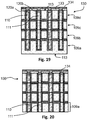
- This modification step can be implemented by thinning the first substrate 109a from its second face 113 ( figure 19 ) until parts of the first and second elements 110, 111 of the first substrate 109a ( figure 20 ). Then ( figure 21 ) the silicide portions 121a, 121b can be formed in the first and second elements 110, 111 of the second end substrate 109a.
- silicide portions 121a, 121b are in particular formed in the manner of those referenced 120a, 120b from a layer of dielectric material 135 deposited on the second end substrate of the stack of substrates (in particular on the face referenced 112 in figure 21 ) and etched in the extension of the first and second elements 110, 111 of the second end substrate 109a.
- the connection element or elements 107 are formed in contact with the silicide elements 121a, 121b ( figure 21 ), and the connecting element (s) 106 are formed in contact with the silicide portions 120a, 120b ( figure 3 ) after removal of the protective layer 134.
- the connecting elements 106 and connecting 107 can be made of aluminum and obtained by PVD deposition (for “physical vapor deposition” in English) followed by photolithography, then etching to delimit them.
- the connecting elements 106 and connecting 107 can be obtained by RDL type electrolysis for “ReDistributionLayer” in English, in this case the connecting elements 106 and connecting 107 can comprise copper and an SnAg alloy, or nickel and gold.
- the dimensions of the pads and the choice of materials for forming them depends on the intended application and the expected temperature difference.
- thermoelectric device can be applied to the manufacturing process allowing it to be obtained, and conversely what applies to the manufacturing process of the thermoelectric device can apply to the thermoelectric device described.
- thermoelectric device as described has an industrial application, in particular in the field of the generation of electrical energy, or in the cooling of electronic components.
- industrial application of such a thermoelectric device can also be extended to any field seeking to exploit a Seebeck effect or a Peltier effect.
- the manufacturing process applies most particularly to the field of microelectronics for manufacturing the associated thermoelectric device.
- thermoelectric device as described can be integrated so as to serve as a power supply for autonomous sensor (s), for microelectronic components, for mobile telephone, for a home automation actuator, for sensor (s) of an intelligent building, for component (s) located in an intelligent electrical network also known under the English name "smart grid", or in the field of the Internet of Things (loT for "Internet of Things” in French English).
- the thermoelectric device has a Seebeck effect, that is to say generates electrical energy, it can be used to serve as an electrical power supply to any component, for example autonomous and not connected to a network of distribution of electricity, by exploiting a temperature difference to which it is subjected.
- thermoelectric device In the case where the thermoelectric device is an electrical energy generator, it can be connected to a DC / DC converter making it possible to convert a direct voltage into another direct voltage of different value. In this case, placing certain thermoelectric junctions in parallel makes it possible to reduce the voltage generated by the thermoelectric device to an input value compatible with the DC / DC converter while maintaining a power equivalent to that of the thermoelectric junctions in series.
Landscapes
- Engineering & Computer Science (AREA)
- Manufacturing & Machinery (AREA)
- Measuring Temperature Or Quantity Of Heat (AREA)
Claims (12)
- Thermoelektrische Vorrichtung (100), aufweisend:- mindestens einen thermoelektrischen Kontakt (103), wobei der thermoelektrische Kontakt (103) ein erstes Klötzchen (101) und ein zweites Klötzchen (102), das mit dem ersten Klötzchen (101) elektrisch verbunden ist, aufweist,- einen Stapel (108) von Substraten, wobei jedes Substrat (109a, 109b, 109c, 109d) mindestens ein erstes Element (110) und mindestens ein zweites Element (111) aufweist, wobei das erste Element (110) und das zweite Element (111) in der Dicke des Substrats (109a, 109b, 109c, 109d) ausgebildet sind,wobei der Stapel (108) von Substraten so beschaffen ist, dass:- das erste Klötzchen (101) des thermoelektrischen Kontakts (103) einen Stapel erster Elemente (110) aufweist,- das zweite Klötzchen (102) des thermoelektrischen Kontakts (103) einen Stapel zweiter Elemente (111) aufweist,wobei der Stapel (108) von Substraten mindestens drei Substrate aufweist, dadurch gekennzeichnet, dass jedes Substrat des Stapels (108) von Substraten, das sich zwischen zwei Endsubstraten (109a, 109d) des Stapels (108) von Substraten befindet, Folgendes aufweist:- eine erste Seite (112),- eine zweite Seite (113), die seiner ersten Seite (112) gegenüberliegt,- eine erste Schicht (114) aus dielektrischem Material, die einen Abschnitt der ersten Seite (112) des Substrats begrenzt,- eine zweite Schicht (115) aus dielektrischem Material, die einen Abschnitt der zweiten Seite (113) des Substrats begrenzt, wobei die erste und zweite Schicht (114, 115) aus dielektrischem Material von dem ersten und zweiten Klötzchen (101, 102) durchquert werden.
- Thermoelektrische Vorrichtung (100) nach dem vorhergehenden Anspruch, dadurch gekennzeichnet, dass für jedes Substrat des Stapels (108) von Substraten, das sich zwischen den zwei Endsubstraten (109a, 109d) des Stapels (108) von Substraten befindet, die erste und zweite Schicht (114, 115) aus dielektrischem Material des Substrats auf und insbesondere beiderseits von einem Träger (117) des Substrats ausgebildet sind.
- Thermoelektrische Vorrichtung (100) nach dem vorhergehenden Anspruch, dadurch gekennzeichnet, dass für jedes Substrat des Stapels (108) von Substraten, das sich zwischen den zwei Endsubstraten (109a, 109d) des Stapels (108) von Substraten befindet, die erste Schicht (114) aus dielektrischem Material des Substrats eine elektrische Leitfähigkeit aufweist, die streng kleiner als jene des Trägers (117) ist, auf dem sie ausgebildet ist, und die zweite Schicht (115) aus dielektrischem Material des Substrats eine elektrische Leitfähigkeit aufweist, die streng kleiner als jene des Trägers (117) ist, auf dem sie ausgebildet ist.
- Thermoelektrische Vorrichtung (100) nach einem der vorhergehenden Ansprüche, dadurch gekennzeichnet, dass der thermoelektrische Kontakt (103) ein elektrisch leitendes Verbindungselement (106) aufweist, das mit einem Teilbereich aus Silicid (120a) des ersten Klötzchens (101) des thermoelektrischen Kontakts (103) und einem Teilbereich aus Silicid (120b) des zweiten Klötzchens (102) des thermoelektrischen Kontakts (103) verbunden ist.
- Thermoelektrische Vorrichtung (100) nach einem der vorhergehenden Ansprüche, dadurch gekennzeichnet, dass jedes Substrat (109a, 109b, 109c, 109d) des Stapels (108) von Substraten Durchkontaktierungen aufweist, die das erste und zweite Element (110, 111) des Substrats (109a, 109b, 109c, 109d) bilden.
- Thermoelektrische Vorrichtung (100) nach einem der vorhergehenden Ansprüche, dadurch gekennzeichnet, dass sie Folgendes aufweist:- erste und zweite Klötzchen (101, 102),- eine Mehrzahl von thermoelektrischen Kontakten (103), jeweils aufweisend eins der ersten Klötzchen (101) und eins der zweiten Klötzchen (102),und dadurch, dass jedes Substrat (109a, 109b, 109c, 109d) erste und zweite Elemente (110, 111) aufweist, wobei der Stapel (108) von Substraten so beschaffen ist, dass:- jedes erste Klötzchen (101) einen Stapel erster Elemente (110) aufweist,- jedes zweite Klötzchen (102) einen Stapel zweiter Elemente (111) aufweist.
- Thermoelektrische Vorrichtung (100) nach dem vorhergehenden Anspruch, dadurch gekennzeichnet, dass die thermoelektrischen Kontakte (103) elektrisch in Reihe geschaltet sind.
- Thermoelektrische Vorrichtung (100) nach Anspruch 6, dadurch gekennzeichnet, dass sie Anordnungen (122) thermoelektrischer Kontakte (103) aufweist, die so beschaffen sind, dass innerhalb jeder Anordnung (122) thermoelektrischer Kontakte (103) die thermoelektrischen Kontakte (103) der Anordnung (122) elektrisch parallel geschaltet sind, wobei die Anordnungen (122) thermoelektrischer Kontakte (103) elektrisch in Reihe geschaltet sind.
- Thermoelektrische Vorrichtung (100) nach einem der vorhergehenden Ansprüche, dadurch gekennzeichnet, dass die Substrate (109a, 109b, 109c, 109d) des Stapels (108) von Substraten durch kovalente Bindungen verbunden sind.
- Verfahren zur Herstellung einer thermoelektrischen Vorrichtung (100) umfassend mindestens einen thermoelektrischen Kontakt (103), das Herstellungsverfahren aufweisend:- einen Schritt des Bereitstellens von Substraten (109), wobei jedes bereitgestellte Substrat (109) mindestens ein erstes Element (110) und mindestens ein zweites Element (111) aufweist, die in seiner Dicke ausgebildet sind,- einen Schritt des Bildens eines Stapels (108) von Substraten unter Verwendung der bereitgestellten Substrate (109), woraus die Bildung eines ersten Klötzchens (101) des thermoelektrischen Kontakts (103) und eines zweiten Klötzchens (102) des thermoelektrischen Kontakts (103) hervorgeht, wobei das erste Klötzchen (101) einen Stapel erster Elemente (110) und das zweite Klötzchen (102) einen Stapel zweiter Elemente (111) aufweist,- einen Schritt des Bildens einer elektrischen Verbindung des thermoelektrischen Kontakts (103), wobei die elektrische Verbindung das erste Klötzchen (101) mit dem zweiten Klötzchen (102) verbindet,wobei der Stapel (108) von Substraten mindestens drei Substrate aufweist, dadurch gekennzeichnet, dass jedes Substrat des Stapels (108) von Substraten, das sich zwischen zwei Endsubstraten (109a, 109d) des Stapels (108) von Substraten befindet, Folgendes aufweist:- eine erste Seite (112),- eine zweite Seite (113), die seiner ersten Seite (112) gegenüberliegt,- eine erste Schicht (114) aus dielektrischem Material, die einen Abschnitt der ersten Seite (112) des Substrats begrenzt,- eine zweite Schicht (115) aus dielektrischem Material, die einen Abschnitt der zweiten Seite (113) des Substrats begrenzt, wobei die erste und zweite Schicht (114, 115) aus dielektrischem Material von dem ersten und zweiten Klötzchen (101, 102) durchquert werden.
- Herstellungsverfahren nach dem vorhergehenden Anspruch, dadurch gekennzeichnet, dass jedes bereitgestellte Substrat (109) so beschaffen ist, dass:- das Substrat (109) eine erste Seite (112) aufweist, in welcher Sacklöcher (124, 125) ausgebildet sind, wobei das erste und zweite Element (110, 111) des Substrats (109) so in den Sacklöchern (124, 125) ausgebildet sind, dass die erste Seite (112) des Substrats (109) Abschnitte (126a, 126b) umfasst, die vom ersten und zweiten Element (110, 111) begrenzt sind,- das Substrat (109) eine zweite Seite (113) aufweist, die seiner ersten Seite (112) gegenüberliegt,und dadurch, dass der Schritt des Bildens des Stapels (108) von Substraten Folgendes aufweist:- einen Schritt des Bildens einer Zusammensetzung (130), umfassend einen Schritt des Inkontaktbringens der ersten Seiten (112) ersten und zweiten Substrats (109a, 109b) aus den bereitgestellten Substraten,- einen Schritt des Veränderns des zweiten Substrats (109b) der Zusammensetzung (130), woraus hervorgeht, dass seine zweite Seite (113) Abschnitte aufweist, die vom ersten und zweiten Element (110, 111) des zweiten Substrats (109b) begrenzt sind, wobei die zweite Seite (113) des veränderten zweiten Substrats (109b) eine Verbindungsseite (131) der Zusammensetzung (130) bildet,- einen Schritt des Veränderns des ersten Substrats (109a), um ein Endsubstrat (109a) des Stapels (108) von Substraten zu bilden.
- Herstellungsverfahren nach dem vorhergehenden Anspruch, dadurch gekennzeichnet, dass es nach dem Schritt des Veränderns des zweiten Substrats (109b) und für jedes bereitgestellte Substrat, das von der Zusammensetzung (130) getrennt ist, genannt das Substrat, das der Zusammensetzung (130) hinzuzufügen ist, einen Schritt des Veränderns der Zusammensetzung (130) aufweist, der Folgendes aufweist:- einen Schritt des Hinzufügens des Substrats (109c), das der Zusammensetzung (130) hinzuzufügen ist, durch Ansetzen der ersten Seite (112) des hinzuzufügenden Substrats (109c) an die Verbindungsseite (131) der Zusammensetzung (130),- einen Schritt des Veränderns des Substrats (109c), das der Zusammensetzung (130) hinzugefügt wurde, woraus hervorgeht, dass seine zweite Seite (113) Abschnitte aufweist, die vom ersten und zweiten Element (110, 111) des Substrats (109c), das der Zusammensetzung (130) hinzugefügt wurde, begrenzt sind, wobei die zweite Seite (113) am Ende des Veränderns des hinzugefügten Substrats (109c) eine neue Verbindungsseite (131) der Zusammensetzung (130) bildet.
Applications Claiming Priority (1)
| Application Number | Priority Date | Filing Date | Title |
|---|---|---|---|
| FR1763343A FR3076401B1 (fr) | 2017-12-28 | 2017-12-28 | Dispositif thermoelectrique et procede de fabrication du dispositif thermoelectrique |
Publications (2)
| Publication Number | Publication Date |
|---|---|
| EP3506375A1 EP3506375A1 (de) | 2019-07-03 |
| EP3506375B1 true EP3506375B1 (de) | 2021-03-10 |
Family
ID=62017443
Family Applications (1)
| Application Number | Title | Priority Date | Filing Date |
|---|---|---|---|
| EP18214810.6A Not-in-force EP3506375B1 (de) | 2017-12-28 | 2018-12-20 | Thermoelektrische vorrichtung und herstellungsverfahren einer solchen thermoelektrischen vorrichtung |
Country Status (2)
| Country | Link |
|---|---|
| EP (1) | EP3506375B1 (de) |
| FR (1) | FR3076401B1 (de) |
Families Citing this family (1)
| Publication number | Priority date | Publication date | Assignee | Title |
|---|---|---|---|---|
| FR3113985A1 (fr) * | 2020-09-08 | 2022-03-11 | Commissariat A L'energie Atomique Et Aux Energies Alternatives | Procede de fabrication d’un dispositif thermoelectrique |
Family Cites Families (3)
| Publication number | Priority date | Publication date | Assignee | Title |
|---|---|---|---|---|
| JP3879769B1 (ja) * | 2006-02-22 | 2007-02-14 | 株式会社村田製作所 | 熱電変換モジュールおよびその製造方法 |
| JPWO2009063805A1 (ja) * | 2007-11-13 | 2011-03-31 | 株式会社村田製作所 | 蓄電機能付き熱電発電装置 |
| WO2014057543A1 (ja) * | 2012-10-10 | 2014-04-17 | 富士通株式会社 | 熱電変換装置および電子装置 |
-
2017
- 2017-12-28 FR FR1763343A patent/FR3076401B1/fr not_active Expired - Fee Related
-
2018
- 2018-12-20 EP EP18214810.6A patent/EP3506375B1/de not_active Not-in-force
Non-Patent Citations (1)
| Title |
|---|
| None * |
Also Published As
| Publication number | Publication date |
|---|---|
| EP3506375A1 (de) | 2019-07-03 |
| FR3076401B1 (fr) | 2020-01-10 |
| FR3076401A1 (fr) | 2019-07-05 |
Similar Documents
| Publication | Publication Date | Title |
|---|---|---|
| EP3657556B1 (de) | Herstellungsverfahren mindestens einer passivierten planaren fotodiode mit reduziertem dunkelstrom | |
| CN111261748B (zh) | 用于制造具有低暗电流的基于锗的二极管阵列的方法 | |
| EP1993138B1 (de) | Transistorvorrichtung mit verspanntem Kanal | |
| EP2840589B1 (de) | Verbessertes Verfahren zur Trennung zwischen einer aktiven Zone eines Substrats und dessen Rückseite oder eines Teilbereichs seiner Rückseite | |
| EP2869342B1 (de) | Verfahren zur Herstellung einer Vorrichtung, die einen integrierten Schaltkreis und Fotovoltaikzellen umfasst und Vorrichtung | |
| EP2577730A2 (de) | Integrierte schaltung mit einem übergangslosen fet mit verarmungsschicht | |
| EP2816597A2 (de) | Herstellungsverfahren einer mechanisch autonomen mikroelektronischen Vorrichtung | |
| EP3506375B1 (de) | Thermoelektrische vorrichtung und herstellungsverfahren einer solchen thermoelektrischen vorrichtung | |
| EP3985745B1 (de) | Verfahren zur herstellung einer thermoelektrischen vorrichtung durch additive fertigung von kämmen, die sich gegenseitig berühren | |
| EP2567415B1 (de) | Modulierbare thermoelektrische vorrichtung | |
| EP2732469B1 (de) | Verfahren zur erzeugung von energie in einer integrierten dreidimensionalen struktur, und entsprechende verbindungsvorrichtung | |
| EP1774588B1 (de) | Zusammenfügen zweier substrate mittels molekularer adhäsion | |
| EP3046143B1 (de) | Verfahren zur herstellung eines dreidimensionalen integrierten schaltkreises | |
| FR3042064B1 (fr) | Dispositif pour connecter au moins un nano-objet associe a une puce permettant une connexion a au moins un systeme electrique externe et son procede de realisation | |
| EP3506358B1 (de) | Thermoelektrische vorrichtung mit thermoelektrischem übergang, der in der dicke eines substrats ausgebildet ist, und herstellungsverfahren dieser thermoelektrischen vorrichtung | |
| EP4355062B1 (de) | Verfahren zur herstellung einer thermoelektrischen struktur | |
| EP4355063B1 (de) | Verfahren zur metallisierung einer thermoelektrischen struktur | |
| WO2022053755A1 (fr) | Procede de fabrication d'un dispositif thermoelectrique | |
| FR2901636A1 (fr) | Connecteur a vias isoles | |
| EP1755164A2 (de) | Methode zur Monatege passiver und aktiver Komponenten und entsprechender integrierter Schaltkreis | |
| FR3166271A1 (fr) | Procédé de fabrication d’un assemblage 3D | |
| EP4505512A1 (de) | Substrat mit vias und zugehörige herstellungsverfahren | |
| FR3160520A1 (fr) | Dispositif monolithique incluant un transistor et un condensateur cointégrés sur un substrat à base de diamant, et procédé de fabrication d’un tel dispositif | |
| FR2979169A1 (fr) | Systèmes semi-conducteurs intégrés en trois dimensions comportant des dispositifs photo-actifs | |
| FR2978610A1 (fr) | Procede de realisation d'une liaison electriquement conductrice traversante et dispositif integre correspondant |
Legal Events
| Date | Code | Title | Description |
|---|---|---|---|
| PUAI | Public reference made under article 153(3) epc to a published international application that has entered the european phase |
Free format text: ORIGINAL CODE: 0009012 |
|
| STAA | Information on the status of an ep patent application or granted ep patent |
Free format text: STATUS: REQUEST FOR EXAMINATION WAS MADE |
|
| 17P | Request for examination filed |
Effective date: 20181220 |
|
| AK | Designated contracting states |
Kind code of ref document: A1 Designated state(s): AL AT BE BG CH CY CZ DE DK EE ES FI FR GB GR HR HU IE IS IT LI LT LU LV MC MK MT NL NO PL PT RO RS SE SI SK SM TR |
|
| AX | Request for extension of the european patent |
Extension state: BA ME |
|
| GRAP | Despatch of communication of intention to grant a patent |
Free format text: ORIGINAL CODE: EPIDOSNIGR1 |
|
| STAA | Information on the status of an ep patent application or granted ep patent |
Free format text: STATUS: GRANT OF PATENT IS INTENDED |
|
| RIC1 | Information provided on ipc code assigned before grant |
Ipc: H01L 35/32 20060101AFI20200214BHEP Ipc: H01L 35/34 20060101ALI20200214BHEP |
|
| INTG | Intention to grant announced |
Effective date: 20200319 |
|
| GRAJ | Information related to disapproval of communication of intention to grant by the applicant or resumption of examination proceedings by the epo deleted |
Free format text: ORIGINAL CODE: EPIDOSDIGR1 |
|
| STAA | Information on the status of an ep patent application or granted ep patent |
Free format text: STATUS: REQUEST FOR EXAMINATION WAS MADE |
|
| INTC | Intention to grant announced (deleted) | ||
| GRAP | Despatch of communication of intention to grant a patent |
Free format text: ORIGINAL CODE: EPIDOSNIGR1 |
|
| STAA | Information on the status of an ep patent application or granted ep patent |
Free format text: STATUS: GRANT OF PATENT IS INTENDED |
|
| INTG | Intention to grant announced |
Effective date: 20201007 |
|
| GRAS | Grant fee paid |
Free format text: ORIGINAL CODE: EPIDOSNIGR3 |
|
| GRAA | (expected) grant |
Free format text: ORIGINAL CODE: 0009210 |
|
| STAA | Information on the status of an ep patent application or granted ep patent |
Free format text: STATUS: THE PATENT HAS BEEN GRANTED |
|
| AK | Designated contracting states |
Kind code of ref document: B1 Designated state(s): AL AT BE BG CH CY CZ DE DK EE ES FI FR GB GR HR HU IE IS IT LI LT LU LV MC MK MT NL NO PL PT RO RS SE SI SK SM TR |
|
| REG | Reference to a national code |
Ref country code: GB Ref legal event code: FG4D Free format text: NOT ENGLISH |
|
| REG | Reference to a national code |
Ref country code: CH Ref legal event code: EP Ref country code: AT Ref legal event code: REF Ref document number: 1370782 Country of ref document: AT Kind code of ref document: T Effective date: 20210315 |
|
| REG | Reference to a national code |
Ref country code: IE Ref legal event code: FG4D Free format text: LANGUAGE OF EP DOCUMENT: FRENCH |
|
| REG | Reference to a national code |
Ref country code: DE Ref legal event code: R096 Ref document number: 602018013689 Country of ref document: DE |
|
| REG | Reference to a national code |
Ref country code: LT Ref legal event code: MG9D |
|
| PG25 | Lapsed in a contracting state [announced via postgrant information from national office to epo] |
Ref country code: GR Free format text: LAPSE BECAUSE OF FAILURE TO SUBMIT A TRANSLATION OF THE DESCRIPTION OR TO PAY THE FEE WITHIN THE PRESCRIBED TIME-LIMIT Effective date: 20210611 Ref country code: HR Free format text: LAPSE BECAUSE OF FAILURE TO SUBMIT A TRANSLATION OF THE DESCRIPTION OR TO PAY THE FEE WITHIN THE PRESCRIBED TIME-LIMIT Effective date: 20210310 Ref country code: FI Free format text: LAPSE BECAUSE OF FAILURE TO SUBMIT A TRANSLATION OF THE DESCRIPTION OR TO PAY THE FEE WITHIN THE PRESCRIBED TIME-LIMIT Effective date: 20210310 Ref country code: BG Free format text: LAPSE BECAUSE OF FAILURE TO SUBMIT A TRANSLATION OF THE DESCRIPTION OR TO PAY THE FEE WITHIN THE PRESCRIBED TIME-LIMIT Effective date: 20210610 Ref country code: NO Free format text: LAPSE BECAUSE OF FAILURE TO SUBMIT A TRANSLATION OF THE DESCRIPTION OR TO PAY THE FEE WITHIN THE PRESCRIBED TIME-LIMIT Effective date: 20210610 Ref country code: LT Free format text: LAPSE BECAUSE OF FAILURE TO SUBMIT A TRANSLATION OF THE DESCRIPTION OR TO PAY THE FEE WITHIN THE PRESCRIBED TIME-LIMIT Effective date: 20210310 |
|
| REG | Reference to a national code |
Ref country code: AT Ref legal event code: MK05 Ref document number: 1370782 Country of ref document: AT Kind code of ref document: T Effective date: 20210310 |
|
| REG | Reference to a national code |
Ref country code: NL Ref legal event code: MP Effective date: 20210310 |
|
| PG25 | Lapsed in a contracting state [announced via postgrant information from national office to epo] |
Ref country code: RS Free format text: LAPSE BECAUSE OF FAILURE TO SUBMIT A TRANSLATION OF THE DESCRIPTION OR TO PAY THE FEE WITHIN THE PRESCRIBED TIME-LIMIT Effective date: 20210310 Ref country code: LV Free format text: LAPSE BECAUSE OF FAILURE TO SUBMIT A TRANSLATION OF THE DESCRIPTION OR TO PAY THE FEE WITHIN THE PRESCRIBED TIME-LIMIT Effective date: 20210310 Ref country code: SE Free format text: LAPSE BECAUSE OF FAILURE TO SUBMIT A TRANSLATION OF THE DESCRIPTION OR TO PAY THE FEE WITHIN THE PRESCRIBED TIME-LIMIT Effective date: 20210310 |
|
| PG25 | Lapsed in a contracting state [announced via postgrant information from national office to epo] |
Ref country code: NL Free format text: LAPSE BECAUSE OF FAILURE TO SUBMIT A TRANSLATION OF THE DESCRIPTION OR TO PAY THE FEE WITHIN THE PRESCRIBED TIME-LIMIT Effective date: 20210310 |
|
| PG25 | Lapsed in a contracting state [announced via postgrant information from national office to epo] |
Ref country code: AT Free format text: LAPSE BECAUSE OF FAILURE TO SUBMIT A TRANSLATION OF THE DESCRIPTION OR TO PAY THE FEE WITHIN THE PRESCRIBED TIME-LIMIT Effective date: 20210310 Ref country code: SM Free format text: LAPSE BECAUSE OF FAILURE TO SUBMIT A TRANSLATION OF THE DESCRIPTION OR TO PAY THE FEE WITHIN THE PRESCRIBED TIME-LIMIT Effective date: 20210310 Ref country code: EE Free format text: LAPSE BECAUSE OF FAILURE TO SUBMIT A TRANSLATION OF THE DESCRIPTION OR TO PAY THE FEE WITHIN THE PRESCRIBED TIME-LIMIT Effective date: 20210310 Ref country code: CZ Free format text: LAPSE BECAUSE OF FAILURE TO SUBMIT A TRANSLATION OF THE DESCRIPTION OR TO PAY THE FEE WITHIN THE PRESCRIBED TIME-LIMIT Effective date: 20210310 |
|
| PG25 | Lapsed in a contracting state [announced via postgrant information from national office to epo] |
Ref country code: IS Free format text: LAPSE BECAUSE OF FAILURE TO SUBMIT A TRANSLATION OF THE DESCRIPTION OR TO PAY THE FEE WITHIN THE PRESCRIBED TIME-LIMIT Effective date: 20210710 Ref country code: PL Free format text: LAPSE BECAUSE OF FAILURE TO SUBMIT A TRANSLATION OF THE DESCRIPTION OR TO PAY THE FEE WITHIN THE PRESCRIBED TIME-LIMIT Effective date: 20210310 Ref country code: PT Free format text: LAPSE BECAUSE OF FAILURE TO SUBMIT A TRANSLATION OF THE DESCRIPTION OR TO PAY THE FEE WITHIN THE PRESCRIBED TIME-LIMIT Effective date: 20210712 Ref country code: RO Free format text: LAPSE BECAUSE OF FAILURE TO SUBMIT A TRANSLATION OF THE DESCRIPTION OR TO PAY THE FEE WITHIN THE PRESCRIBED TIME-LIMIT Effective date: 20210310 Ref country code: SK Free format text: LAPSE BECAUSE OF FAILURE TO SUBMIT A TRANSLATION OF THE DESCRIPTION OR TO PAY THE FEE WITHIN THE PRESCRIBED TIME-LIMIT Effective date: 20210310 |
|
| REG | Reference to a national code |
Ref country code: DE Ref legal event code: R097 Ref document number: 602018013689 Country of ref document: DE |
|
| PLBE | No opposition filed within time limit |
Free format text: ORIGINAL CODE: 0009261 |
|
| STAA | Information on the status of an ep patent application or granted ep patent |
Free format text: STATUS: NO OPPOSITION FILED WITHIN TIME LIMIT |
|
| PG25 | Lapsed in a contracting state [announced via postgrant information from national office to epo] |
Ref country code: ES Free format text: LAPSE BECAUSE OF FAILURE TO SUBMIT A TRANSLATION OF THE DESCRIPTION OR TO PAY THE FEE WITHIN THE PRESCRIBED TIME-LIMIT Effective date: 20210310 Ref country code: DK Free format text: LAPSE BECAUSE OF FAILURE TO SUBMIT A TRANSLATION OF THE DESCRIPTION OR TO PAY THE FEE WITHIN THE PRESCRIBED TIME-LIMIT Effective date: 20210310 Ref country code: AL Free format text: LAPSE BECAUSE OF FAILURE TO SUBMIT A TRANSLATION OF THE DESCRIPTION OR TO PAY THE FEE WITHIN THE PRESCRIBED TIME-LIMIT Effective date: 20210310 |
|
| 26N | No opposition filed |
Effective date: 20211213 |
|
| PG25 | Lapsed in a contracting state [announced via postgrant information from national office to epo] |
Ref country code: SI Free format text: LAPSE BECAUSE OF FAILURE TO SUBMIT A TRANSLATION OF THE DESCRIPTION OR TO PAY THE FEE WITHIN THE PRESCRIBED TIME-LIMIT Effective date: 20210310 |
|
| PG25 | Lapsed in a contracting state [announced via postgrant information from national office to epo] |
Ref country code: IT Free format text: LAPSE BECAUSE OF FAILURE TO SUBMIT A TRANSLATION OF THE DESCRIPTION OR TO PAY THE FEE WITHIN THE PRESCRIBED TIME-LIMIT Effective date: 20210310 |
|
| PG25 | Lapsed in a contracting state [announced via postgrant information from national office to epo] |
Ref country code: IS Free format text: LAPSE BECAUSE OF FAILURE TO SUBMIT A TRANSLATION OF THE DESCRIPTION OR TO PAY THE FEE WITHIN THE PRESCRIBED TIME-LIMIT Effective date: 20210710 |
|
| PG25 | Lapsed in a contracting state [announced via postgrant information from national office to epo] |
Ref country code: MC Free format text: LAPSE BECAUSE OF FAILURE TO SUBMIT A TRANSLATION OF THE DESCRIPTION OR TO PAY THE FEE WITHIN THE PRESCRIBED TIME-LIMIT Effective date: 20210310 |
|
| REG | Reference to a national code |
Ref country code: CH Ref legal event code: PL |
|
| REG | Reference to a national code |
Ref country code: BE Ref legal event code: MM Effective date: 20211231 |
|
| PG25 | Lapsed in a contracting state [announced via postgrant information from national office to epo] |
Ref country code: LU Free format text: LAPSE BECAUSE OF NON-PAYMENT OF DUE FEES Effective date: 20211220 Ref country code: IE Free format text: LAPSE BECAUSE OF NON-PAYMENT OF DUE FEES Effective date: 20211220 |
|
| REG | Reference to a national code |
Ref country code: DE Ref legal event code: R079 Ref document number: 602018013689 Country of ref document: DE Free format text: PREVIOUS MAIN CLASS: H01L0035320000 Ipc: H10N0010170000 |
|
| PG25 | Lapsed in a contracting state [announced via postgrant information from national office to epo] |
Ref country code: BE Free format text: LAPSE BECAUSE OF NON-PAYMENT OF DUE FEES Effective date: 20211231 |
|
| PG25 | Lapsed in a contracting state [announced via postgrant information from national office to epo] |
Ref country code: LI Free format text: LAPSE BECAUSE OF NON-PAYMENT OF DUE FEES Effective date: 20211231 Ref country code: CH Free format text: LAPSE BECAUSE OF NON-PAYMENT OF DUE FEES Effective date: 20211231 |
|
| PGFP | Annual fee paid to national office [announced via postgrant information from national office to epo] |
Ref country code: GB Payment date: 20221223 Year of fee payment: 5 Ref country code: FR Payment date: 20221222 Year of fee payment: 5 |
|
| PGFP | Annual fee paid to national office [announced via postgrant information from national office to epo] |
Ref country code: DE Payment date: 20221221 Year of fee payment: 5 |
|
| PG25 | Lapsed in a contracting state [announced via postgrant information from national office to epo] |
Ref country code: CY Free format text: LAPSE BECAUSE OF FAILURE TO SUBMIT A TRANSLATION OF THE DESCRIPTION OR TO PAY THE FEE WITHIN THE PRESCRIBED TIME-LIMIT Effective date: 20210310 |
|
| PG25 | Lapsed in a contracting state [announced via postgrant information from national office to epo] |
Ref country code: HU Free format text: LAPSE BECAUSE OF FAILURE TO SUBMIT A TRANSLATION OF THE DESCRIPTION OR TO PAY THE FEE WITHIN THE PRESCRIBED TIME-LIMIT; INVALID AB INITIO Effective date: 20181220 |
|
| PG25 | Lapsed in a contracting state [announced via postgrant information from national office to epo] |
Ref country code: MK Free format text: LAPSE BECAUSE OF FAILURE TO SUBMIT A TRANSLATION OF THE DESCRIPTION OR TO PAY THE FEE WITHIN THE PRESCRIBED TIME-LIMIT Effective date: 20210310 |
|
| REG | Reference to a national code |
Ref country code: DE Ref legal event code: R119 Ref document number: 602018013689 Country of ref document: DE |
|
| GBPC | Gb: european patent ceased through non-payment of renewal fee |
Effective date: 20231220 |
|
| PG25 | Lapsed in a contracting state [announced via postgrant information from national office to epo] |
Ref country code: MT Free format text: LAPSE BECAUSE OF FAILURE TO SUBMIT A TRANSLATION OF THE DESCRIPTION OR TO PAY THE FEE WITHIN THE PRESCRIBED TIME-LIMIT Effective date: 20210310 |
|
| PG25 | Lapsed in a contracting state [announced via postgrant information from national office to epo] |
Ref country code: DE Free format text: LAPSE BECAUSE OF NON-PAYMENT OF DUE FEES Effective date: 20240702 |
|
| PG25 | Lapsed in a contracting state [announced via postgrant information from national office to epo] |
Ref country code: GB Free format text: LAPSE BECAUSE OF NON-PAYMENT OF DUE FEES Effective date: 20231220 |
|
| PG25 | Lapsed in a contracting state [announced via postgrant information from national office to epo] |
Ref country code: FR Free format text: LAPSE BECAUSE OF NON-PAYMENT OF DUE FEES Effective date: 20231231 |
|
| PG25 | Lapsed in a contracting state [announced via postgrant information from national office to epo] |
Ref country code: GB Free format text: LAPSE BECAUSE OF NON-PAYMENT OF DUE FEES Effective date: 20231220 Ref country code: FR Free format text: LAPSE BECAUSE OF NON-PAYMENT OF DUE FEES Effective date: 20231231 Ref country code: DE Free format text: LAPSE BECAUSE OF NON-PAYMENT OF DUE FEES Effective date: 20240702 |
|
| PG25 | Lapsed in a contracting state [announced via postgrant information from national office to epo] |
Ref country code: TR Free format text: LAPSE BECAUSE OF FAILURE TO SUBMIT A TRANSLATION OF THE DESCRIPTION OR TO PAY THE FEE WITHIN THE PRESCRIBED TIME-LIMIT Effective date: 20210310 |