EP3582244B1 - Photoelektrischer sensor und lichtprojektor - Google Patents
Photoelektrischer sensor und lichtprojektor Download PDFInfo
- Publication number
- EP3582244B1 EP3582244B1 EP17895919.3A EP17895919A EP3582244B1 EP 3582244 B1 EP3582244 B1 EP 3582244B1 EP 17895919 A EP17895919 A EP 17895919A EP 3582244 B1 EP3582244 B1 EP 3582244B1
- Authority
- EP
- European Patent Office
- Prior art keywords
- light
- power supply
- supply line
- output signal
- photoelectric sensor
- Prior art date
- Legal status (The legal status is an assumption and is not a legal conclusion. Google has not performed a legal analysis and makes no representation as to the accuracy of the status listed.)
- Active
Links
Images


Classifications
-
- H—ELECTRICITY
- H03—ELECTRONIC CIRCUITRY
- H03K—PULSE TECHNIQUE
- H03K17/00—Electronic switching or gating, i.e. not by contact-making and –breaking
- H03K17/94—Electronic switching or gating, i.e. not by contact-making and –breaking characterised by the way in which the control signals are generated
- H03K17/941—Electronic switching or gating, i.e. not by contact-making and –breaking characterised by the way in which the control signals are generated using an optical detector
-
- G—PHYSICS
- G01—MEASURING; TESTING
- G01S—RADIO DIRECTION-FINDING; RADIO NAVIGATION; DETERMINING DISTANCE OR VELOCITY BY USE OF RADIO WAVES; LOCATING OR PRESENCE-DETECTING BY USE OF THE REFLECTION OR RERADIATION OF RADIO WAVES; ANALOGOUS ARRANGEMENTS USING OTHER WAVES
- G01S7/00—Details of systems according to groups G01S13/00, G01S15/00, G01S17/00
- G01S7/48—Details of systems according to groups G01S13/00, G01S15/00, G01S17/00 of systems according to group G01S17/00
- G01S7/481—Constructional features, e.g. arrangements of optical elements
- G01S7/4811—Constructional features, e.g. arrangements of optical elements common to transmitter and receiver
- G01S7/4812—Constructional features, e.g. arrangements of optical elements common to transmitter and receiver transmitted and received beams following a coaxial path
-
- G—PHYSICS
- G01—MEASURING; TESTING
- G01V—GEOPHYSICS; GRAVITATIONAL MEASUREMENTS; DETECTING MASSES OR OBJECTS; TAGS
- G01V8/00—Prospecting or detecting by optical means
- G01V8/10—Detecting, e.g. by using light barriers
-
- G—PHYSICS
- G01—MEASURING; TESTING
- G01S—RADIO DIRECTION-FINDING; RADIO NAVIGATION; DETERMINING DISTANCE OR VELOCITY BY USE OF RADIO WAVES; LOCATING OR PRESENCE-DETECTING BY USE OF THE REFLECTION OR RERADIATION OF RADIO WAVES; ANALOGOUS ARRANGEMENTS USING OTHER WAVES
- G01S17/00—Systems using the reflection or reradiation of electromagnetic waves other than radio waves, e.g. lidar systems
- G01S17/02—Systems using the reflection of electromagnetic waves other than radio waves
- G01S17/04—Systems determining the presence of a target
-
- G—PHYSICS
- G05—CONTROLLING; REGULATING
- G05B—CONTROL OR REGULATING SYSTEMS IN GENERAL; FUNCTIONAL ELEMENTS OF SUCH SYSTEMS; MONITORING OR TESTING ARRANGEMENTS FOR SUCH SYSTEMS OR ELEMENTS
- G05B19/00—Program-control systems
- G05B19/02—Program-control systems electric
- G05B19/04—Program control other than numerical control, i.e. in sequence controllers or logic controllers
- G05B19/05—Programmable logic controllers, e.g. simulating logic interconnections of signals according to ladder diagrams or function charts
- G05B19/058—Safety, monitoring
-
- H—ELECTRICITY
- H01—ELECTRIC ELEMENTS
- H01H—ELECTRIC SWITCHES; RELAYS; SELECTORS; EMERGENCY PROTECTIVE DEVICES
- H01H35/00—Switches operated by change of a physical condition
-
- G—PHYSICS
- G01—MEASURING; TESTING
- G01N—INVESTIGATING OR ANALYSING MATERIALS BY DETERMINING THEIR CHEMICAL OR PHYSICAL PROPERTIES
- G01N21/00—Investigating or analysing materials by the use of optical means, i.e. using sub-millimetre waves, infrared, visible or ultraviolet light
- G01N21/84—Systems specially adapted for particular applications
- G01N2021/845—Objects on a conveyor
-
- G—PHYSICS
- G01—MEASURING; TESTING
- G01N—INVESTIGATING OR ANALYSING MATERIALS BY DETERMINING THEIR CHEMICAL OR PHYSICAL PROPERTIES
- G01N21/00—Investigating or analysing materials by the use of optical means, i.e. using sub-millimetre waves, infrared, visible or ultraviolet light
- G01N21/84—Systems specially adapted for particular applications
-
- G—PHYSICS
- G05—CONTROLLING; REGULATING
- G05B—CONTROL OR REGULATING SYSTEMS IN GENERAL; FUNCTIONAL ELEMENTS OF SUCH SYSTEMS; MONITORING OR TESTING ARRANGEMENTS FOR SUCH SYSTEMS OR ELEMENTS
- G05B2219/00—Program-control systems
- G05B2219/10—Plc systems
- G05B2219/16—Plc to applications
- G05B2219/163—Domotique, domestic, home control, automation, smart, intelligent house
-
- H—ELECTRICITY
- H03—ELECTRONIC CIRCUITRY
- H03K—PULSE TECHNIQUE
- H03K2217/00—Indexing scheme related to electronic switching or gating, i.e. not by contact-making or -breaking covered by H03K17/00
- H03K2217/94—Indexing scheme related to electronic switching or gating, i.e. not by contact-making or -breaking covered by H03K17/00 characterised by the way in which the control signal is generated
- H03K2217/941—Indexing scheme related to electronic switching or gating, i.e. not by contact-making or -breaking covered by H03K17/00 characterised by the way in which the control signal is generated using an optical detector
- H03K2217/94102—Indexing scheme related to electronic switching or gating, i.e. not by contact-making or -breaking covered by H03K17/00 characterised by the way in which the control signal is generated using an optical detector characterised by the type of activation
- H03K2217/94104—Indexing scheme related to electronic switching or gating, i.e. not by contact-making or -breaking covered by H03K17/00 characterised by the way in which the control signal is generated using an optical detector characterised by the type of activation using a light barrier
Definitions
- the present invention relates to a transmission-type photoelectric sensor and a light emitter included in the photoelectric sensor.
- a photoelectric sensor includes: a light emitting unit configured to emit a light beam; and a light receiving unit configured to detect that the emitted light beam has changed due to a detection target.
- the photoelectric sensor is classified roughly into a transmission type, a reflection type, a distance-setting type, and the like. Among them, in a reflection-type photoelectric sensor and a distance-setting-type photoelectric sensor, a light emitting unit and a light receiving unit are disposed approximately at the same position. In contrast, in a transmission-type photoelectric sensor, a light emitting unit and a light receiving unit are spaced apart from each other.
- Various types of sensors each including a photoelectric sensor each serve as a key device for implementing factory automation (FA). Based on the detection results from various types of sensors, the behaviors of various types of devices and facilities are controlled. Also, some defects may occur in various types of sensors. In such a case, occurrence of such defects needs to be detected.
- FA factory automation
- Japanese Patent Laying-Open No. 2009-098735 discloses a slave of a PLC, by which an abnormality in a photoelectric sensor can be detected in real time while reducing the burden on a user program on the PLC side for executing a sensor abnormality diagnosing method utilizing a function of changing the amount of emitted light beam in a sensing system in which a plurality of transmission-type photoelectric sensors are connected to a PLC through the slave.
- the sensor abnormality diagnosing means mounted in the slave of the PLC disclosed in PTL 1 is configured to change the amount of emitted light beam and detect an abnormality in a photoelectric sensor based on the relation of the amount of light beam received at that time.
- US 5 532 471 A discloses a photoelectric switch including a light emitting section emitting pulse light so that intensity of the emitted pulse light is sequentially increased.
- a light detecting section detects the pulse light emitted by the light emitting section.
- a light detection signal indicative of the received light is amplified and then integrated.
- a high-level light detection signal is delivered by the light detecting section when an integral value is equal to or above a threshold.
- a determination circuit delivers a first detection signal when a duration of the light detection signal is equal or above a predetermined values.
- the determination circuit further delivers a stable operation signal when a set time period is reached.
- the light detecting section is integrated into one-chip configuration.
- sensor abnormality diagnosing means needs to be mounted in the slave of the PLC, which is suitable when a large number of transmission-type photoelectric sensors are connected through a single slave, but is not advantageous in terms of cost when a transmission-type photoelectric sensor is connected alone.
- An object of the present invention is to implement a transmission-type photoelectric sensor configured to allow detection of an abnormality in a simple configuration.
- a photoelectric sensor including a light emitter and a light receiver
- the light emitter includes: a light emitting unit configured to emit a light beam, and a power supply circuit configured to receive supply of electric power through a first power supply line leading to an outside of the light emitter and to supply required electric power to the light emitting unit.
- the light receiver includes: a first switching element, connected to a second power supply line leading to an outside of the light receiver, for serving to output a first output signal via a first signal line; a second switching element, connected to the second power supply line, for serving to output a second output signal via a second signal line; and a detection circuit configured to switch a conducting state of each of the first switching element and the second switching element in accordance with an intensity of light detected.
- the detection circuit is configured to switch the first switching element and the second switching element so as to be brought into conducting states different from each other in accordance with the intensity of light detected.
- a third power supply line is provided such that one end of the third power supply line is electrically connected to the first power supply line inside the light emitter and the other end of the third power supply line is electrically connected to the second power supply line outside the light receiver.
- the light emitter further includes a third switching element disposed such that one side of the third switching element is connected to the one end of the third power supply line and the other side of the third switching element is connected to the first power supply line, and a monitoring circuit configured to control a conducting state of the third switching element.
- the monitoring circuit is configured to operate with electric power supplied through the first power supply line and to maintain the third switching element in a conducting state as long as electric power is supplied through the first power supply line.
- the first output signal and the second output signal are normally maintained in alternating low and high states, but are both in a low state at least either when light is detected or when light is not detected by the detection circuit and when at least one of the second power supply line, a ground line of the light receiver, the first signal line, the first power supply line, and a ground line of the light emitter is disconnected, such that an abnormality can be detected when both the first output signal and the second output signal are in the low state.
- the light emitter further includes a detector configured to monitor a state of the light beam applied from the light emitting unit.
- the monitoring circuit is configured to maintain the third switching element in the conducting state only as long both power is supplied through the first power supply line and the light beam is applied in a predetermined state.
- the photoelectric sensor further includes a connection unit through which electric power is input from an external power supply and through which the first output signal and the second output signal are output.
- the first power supply line extends from the light emitter to the connection unit.
- the second power supply line extends from the light receiver to the connection unit.
- the light emitter and the light receiver are separated from each other and in combination form the photoelectric sensor
- the present invention can implement a transmission-type photoelectric sensor that is capable of detecting an abnormality in a simple configuration.
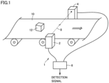
- Fig. 1 is a schematic diagram showing the state where transmission-type photoelectric sensor 1 according to the present embodiment is disposed.
- Fig. 1 shows an example of detecting a workpiece 12 that is conveyed on a conveyor 10.
- photoelectric sensor 1 includes a light emitter 2, a light receiver 4, and a controller 6.
- Light emitter 2 and light receiver 4 excluding controller 6 may also be referred to as a "photoelectric sensor”.
- Light emitter 2 and light receiver 4 are separated from each other and disposed such that light receiver 4 receives a light beam 8 emitted from light emitter 2. In other words, light emitter 2 and light receiver 4 are provided as separate housings.
- the state of light receiver 4 receiving the light beam changes. Then, based on this change, the presence or absence of workpiece 12 can be detected.
- Controller 6 may issue commands for controlling the timing and the state for applying light beam 8 from light emitter 2, as will be described later.
- Fig. 2 is a schematic diagram showing the configuration of transmission-type photoelectric sensor 1 according to the present embodiment.
- light emitter 2 of photoelectric sensor 1 includes a light emitting unit 22 and a power supply circuit 24.
- Power supply circuit 24 receives electric power supplied from an external power supply and supplies required electric power of a prescribed voltage to light emitting unit 22.
- Light emitting unit 22 is for example formed of a light emitting element such as a light emitting diode (LED), a lens and the like, and configured to emit light beam 8 to be applied to a detection target.
- LED light emitting diode
- Light receiver 4 of photoelectric sensor 1 includes a light receiving unit 42, a detection circuit 44, and a signal output circuit 46.
- Light receiving unit 42 is formed of a light receiving element such as a photodiode.
- detection circuit 44 outputs a signal appropriate to the light-beam incident state and/or the light-beam interrupted state.
- signal output circuit 46 outputs a detection signal to controller 6 ( Fig. 1 ) and the like.
- Fig. 3 is a schematic diagram showing an example of the wiring configuration of photoelectric sensor 101 according to the related art of the present invention.
- photoelectric sensor 101 according to the related art of the present invention includes a light emitter 102 and a light receiver 104, each of which supplies electric power and outputs a signal through a connection unit 130.
- electric power is input to connection unit 130 from an external power supply while output signals OUT1 and OUT2 (the first output signal and the second output signal) are output from connection unit 130.
- Light emitting unit 22 of light emitter 102 is substantially the same as light emitting unit 22 of light emitter 2 in photoelectric sensor 1.
- Light receiving unit 42, detection circuit 44 and signal output circuit 46 of light receiver 104 are substantially the same as light receiving unit 42, detection circuit 44 and signal output circuit 46, respectively, of light receiver 4.
- Power supply circuit 124 of light emitter 102 receives electric power supplied from an external power supply, and supplies electric power of a prescribed voltage to light emitting unit 22.
- Each of photoelectric sensor 101 according to the related art of the present invention and photoelectric sensor 1 according to the present embodiment (which will be described later in detail) outputs two signals as detection signals. By using such two signals, any defect that may occur in light receiver 104 and light receiver 4 can be detected. A method of detecting such a defect will be described later in detail.
- a power supply potential VCC supplied to connection unit 130 is connected to one end of power supply circuit 124 of light emitter 102 through power supply line 131, and a ground potential GND supplied to connection unit 130 is connected to the other end of power supply circuit 124 of light emitter 102 through a ground line 132.
- connection unit 130 In the wiring configuration of light receiver 104, power supply potential VCC supplied to connection unit 130 is connected to one end of signal output circuit 46 of light receiver 104 through power supply line 133, and ground potential GND supplied to connection unit 130 is connected to the other end of signal output circuit 46 of light receiver 104 through ground line 134.
- the electric power supplied through power supply line 133 and ground line 134 may be supplied to detection circuit 44.
- a power supply circuit that is not shown is also connected to power supply line 133 and ground line 134.
- a transistor 462 and a transistor 466 are connected in parallel with power supply potential VCC supplied to signal output circuit 46.
- Transistor 462 has one end connected to a first signal line 135.
- the electric potential appearing on first signal line 135 is defined as an output signal OUT1.
- transistor 462 corresponds to the first switching element connected to power supply line 133 (the second power supply line) leading to the outside of light receiver 104 and serving to output the output signal OUT1 (the first output signal).
- transistor 466 has one end connected to second signal line 136.
- the electric potential appearing on second signal line 136 is defined as an output signal OUT2.
- transistor 466 corresponds to the second switching element connected to power supply line 133 (the second power supply line) leading to the outside of light receiver 104 and serving to output the output signal OUT2 (the second output signal).
- photoelectric sensor 1 in which the values inverted from each other are output as two output signals in accordance with the intensity of light. In other words, two signals inverted from each other are output as detection signals.
- Transistor 462 has a gate to which a drive line 442 from detection circuit 44 is connected.
- Transistor 466 has a gate to which a drive line 446 connected to drive line 442 through an inverting circuit 444 is input.
- Detection circuit 44 drives drive line 442 in response to the detection signal from light receiving unit 42.
- Drive line 446 is connected to the output of inverting circuit 444 to which drive line 442 is input. Accordingly, drive line 442 and drive line 446 are driven complementarily to each other.
- drive line 442 is activated while drive line 446 is deactivated.
- drive line 442 is deactivated while drive line 446 is activated. In this way, one drive line is activated while the other drive line is deactivated.
- detection circuit 44 switches transistor 462 (the first switching element) and transistor 466 (the second switching element) so as to be brought into conducting states different from each other.
- detection circuit 44 switches the conducting state of each of transistor 462 (the first switching element) and transistor 466 (the second switching element).
- output signal OUT1 when output signal OUT1 is at Hi (in an active state/at a high potential) in the state where a prescribed amount of received light is detected by light receiving unit 42, output signal OUT2 is at Low (in a non-active state/at a low potential).
- output signal OUT1 when a prescribed amount of received light is not detected by light receiving unit 42, output signal OUT1 is at Low and output signal OUT2 is at Hi.
- output signal OUT1 and output signal OUT2 may be opposite. Specifically, when output signal OUT1 is at Low (in a non-active state/at a low potential) in the state where a prescribed amount of received light is detected by light receiving unit 42, output signal OUT2 is at Hi (in an active state/at a high potential).
- controller 6 (see Fig. 1 ), occurrence or non-occurrence of an abnormality can be detected based on the combination of the value of output signal OUT1 and the value of output signal OUT2.
- Light emitter 102 and light receiver 104 may be connected through a terminal provided in connection unit 130.
- the configuration formed by connecting a plurality of cables may be employed as a cable that connects connection unit 130 and light emitter 102 and/or a cable that connects connection unit 130 and light receiver 104. In such a case, connection is achieved through optional connectors between a cable and connection unit 130, between cables, and between a cable and light emitter 102 or light receiver 104.
- connection unit 130 there is a possibility that disconnection may occur in a conductive wire that connects connection unit 130 and light emitter 102 or light receiver 104.
- disconnection may occur in a conductive wire that connects connection unit 130 and light emitter 102 or light receiver 104.
- the possibility of occurrence of disconnection becomes higher.
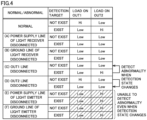
- Fig. 4 is a diagram showing changes in output signals at the time when disconnection occurs in photoelectric sensor 101 according to the related art of the present invention. Fig.
- output signal OUT1 is at Hi and output signal OUT2 is at Low when a detection target does not exist (the light-beam incident state: no detection target exists), whereas output signal OUT1 is at Low and output signal OUT2 is at Hi when a detection target exists (the light-beam interrupted state: a detection target exists). Based on these output signals, it is determined whether a detection target exists or not.
- Transmission-type photoelectric sensor 1 provides a configuration that allows detection of disconnection that may occur in a conductive wire connected to light emitter 102, as described above.
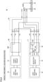
- Fig. 5 is a schematic diagram showing an example of the wiring configuration of photoelectric sensor 1 according to the present embodiment.
- photoelectric sensor 1 according to the present embodiment includes a light emitter 2 and a light receiver 4, each of which supplies electric power and outputs a signal through a connection unit 30.
- Photoelectric sensor 1 outputs two signals that are inverted from each other as detection signals. By using these two signals inverted from each other, a defect that may occur not only in light receiver 4 but also in light emitter 2 can be detected. The method of detecting such a defect will be described later in detail.
- Light emitter 2 includes a signal output circuit 26 in addition to light emitting unit 22 and power supply circuit 24. Signal output circuit 26 serves to output a signal in accordance with the state of light emitter 2.
- power supply potential VCC supplied to connection unit 30 is input into signal output circuit 26 of light emitter 2 through power supply line 31, and is also connected to one end of power supply circuit 24.
- Ground potential GND supplied to connection unit 30 is input into signal output circuit 26 of light emitter 2 through ground line 32 and also connected to the other end of power supply circuit 24.
- power supply circuit 24 of light emitter 2 receives supply of electric power through power supply line 31 (the first power supply line) and ground line 32, each of which leads to the outside of light emitter 2.
- power supply line 31 and ground line 32 extend to connection unit 30.
- a transistor 262 is connected to power supply potential VCC to be supplied to signal output circuit 26.
- Power supply circuit 24 of light emitter 2 includes a monitoring circuit 25 that is also operated with electric power supplied through power supply line 31 (the first power supply line) and ground line 32.
- a drive line 266 is disposed between the gate of transistor 262 and monitoring circuit 25.
- Monitoring circuit 25 controls the conducting state of transistor 262 (the third switching element). In other words, monitoring circuit 25 activates or deactivates drive line 266 in accordance with the state of light emitter 2. More specifically, monitoring circuit 25 maintains drive line 266 in the activated state as long as light emitter 2 is in a sound state or as long as electric power is supplied to power supply circuit 24.
- a secondary power supply line 38 is connected to a power supply line 33 of light receiver 4 in connection unit 30.
- power supply potential VCC supplied to signal output circuit 26 passes through transistor 262 of signal output circuit 26, and thereafter is supplied to signal output circuit 46 through secondary power supply line 38 and power supply line 33.
- light receiver 4 includes transistor 262 (the third switching element) disposed between one end of secondary power supply line 38 (the third power supply line) and power supply line 31 (the first power supply line).
- photoelectric sensor 1 is provided with secondary power supply line 38 (the third power supply line) that has: one end electrically connected to power supply line 31 (the first power supply line) on the inside of light emitter 2; and the other end electrically connected to power supply line 33 (the second power supply line) on the outside of light receiver 4.
- Power supply line 33 (the second power supply line) and ground line 34 extend to connection unit 30.
- occurrence or non-occurrence of an abnormality can be detected based on the combination of the value of output signal OUT1 and the value output signal OUT2.
- An example of such an abnormality to be detected may be disconnection that occurs in a conductive wire connecting connection unit 30 to light emitter 2 or light receiver 4, as described above.
- Fig. 6 is a diagram showing changes in output signals at the time when disconnection occurs in photoelectric sensor 1 according to the present embodiment.
- Fig. 6 shows the output results of output signal OUT1 and output signal OUT2 in the each of state where a detection target does not exist (the light-beam incident state) and the state where a detection target exists (the light-beam interrupted state) with regard to each of the normal state where no disconnection occurs; (A) the case where power supply line 33 of light receiver 4 is disconnected; (B) the case where ground line 34 of light receiver 4 is disconnected; (C) the case where first signal line 35 is disconnected; (D) the case where second signal line 36 is disconnected; (E) the case where power supply line 31 of light emitter 2 is disconnected; (F) the case where ground line 32 of light emitter 2 is disconnected; and (G) the case where secondary power supply line 38 of light emitter 2 is disconnected.
- photoelectric sensor 1 in the normal state where no disconnection occurs, can determine whether a detection target exists or not based on output signal OUT1 and output signal OUT2, as in photoelectric sensor 101 according to the related art as described above.
- photoelectric sensor 1 can detect that an abnormality occurs in each of (A) the case where power supply line 33 of light receiver 4 is disconnected; (B) the case where ground line 34 of light receiver 4 is disconnected; (C) the case where first signal line 35 is disconnected; and (D) the case where second signal line 36 is disconnected, as in photoelectric sensor 101 according to the related art as described above.
- photoelectric sensor 1 can detect that an abnormality occurs in each of: (E) the case where power supply line 31 of light emitter 2 is disconnected; and (F) ground line 32 of light emitter 2 is disconnected, in contrast to photoelectric sensor 101 according to the related art as described above.
- Photoelectric sensor 1 according to the present embodiment is different from photoelectric sensor 101 shown in Fig. 3 in that secondary power supply line 38 is added as a conductive wire that connects connection unit 30 and light emitter 2. Although this secondary power supply line 38 also may be disconnected, such disconnection of secondary power supply line 38 can also be detected.
- photoelectric sensor 1 can reliably detect an abnormality even when disconnection occurs in any of: the conductive wire that connects connection unit 30 and light emitter 2; and the conductive wire that connects connection unit 30 and light receiver 4.
- Monitoring circuit 25 of power supply circuit 24 shown in Fig. 5 may be configured to more precisely monitor the state of light emitter 2. Examples of conceivable situations may be: a situation where the lens surface (a surface onto which a light beam is applied) of light emitting unit 22 of light emitter 2 is stained; and a situation where the amount of light flux from a light emitting element that forms light emitting unit 22 is reduced due to the end of its lifespan. Monitoring circuit 25 may include a function of detecting such an abnormal situation.
- Fig. 7 is a schematic diagram showing an example of the wiring configuration of a photoelectric sensor 1A according to the first modification of the present embodiment.
- photoelectric sensor 1A according to the first modification of the present embodiment includes a light-beam applying state detection sensor 23 that is disposed in close proximity to light emitting unit 22 of light emitter 2A.
- Light-beam applying state detection sensor 23 corresponds to a detector that monitors the state of light beam 8 applied from light emitting unit 22.
- light-beam applying state detection sensor 23 is formed of a photodiode and the like and configured to determine whether or not the intensity or the illuminance of light beam 8 applied from light emitting unit 22 of light emitter 2A is equal to or greater than a prescribed value, and then, output the detection result to a monitoring circuit 25A.
- Monitoring circuit 25A maintains transistor 262 (the third switching element) in the conducting state when light beam 8 is applied in a predetermined state. More specifically, monitoring circuit 25A shifts drive line 266 to a non-active state (Low) when the detection result from light-beam applying state detection sensor 23 shows that the intensity of light beam 8 is less than a prescribed value even though prescribed electric power is supplied from power supply circuit 24 to light emitting unit 22. This brings transistor 262 into a non-conducting state, so that a path through which electric power is supplied to light receiver 4 is interrupted. As a result, irrespective of the presence or absence of a detection target, each of output signal OUT1 and output signal OUT2 is set at Low, which is to be detected as an abnormality.
- a non-active state Low
- Fig. 7 shows an example of monitoring the intensity of light beam 8 applied from light emitting unit 22 of light emitter 2A as a representative example. Without being limited to this example, any state of light emitter 2 may be monitored. Examples of a target to be monitored may be the ambient temperature, the internal temperature, the quality of the external power supply (a voltage value, a voltage change rate, and the like), the capacitance of an electrolytic capacitor mounted in power supply circuit 24, and the like.
- the voltage of a light emitting circuit may be monitored. Breakdown to open of a light emitting element such as an LED causes a decrease in the drive voltage of the light emitting circuit. Thus, while monitoring such a voltage decrease, the output signal from a light emitter may be set at Low.
- Photoelectric sensor 1 employs a configuration in which an abnormality such as disconnection is detected by disposing light emitter 2 and light receiver 4 so as to be involved in a portion of the path until which output signal OUT1 and output signal OUT2 are output.
- the circuit configuration in light emitter 2 may be further simplified. The following is an explanation about an example in which the circuit configuration of light emitter 2 is simplified.
- Fig. 8 is a schematic diagram showing an example of the wiring configuration of a photoelectric sensor 1B according to the second modification of the present embodiment.
- the circuit configuration of a signal output circuit 26B of a light emitter 2B is simplified. More specifically, transistor 262 and the like are not provided and one end of secondary power supply line 38 is electrically connected to power supply line 31. In even such a simple circuit configuration, disconnection occurring in power supply line 31 and the like can be detected.
- connection unit 30 that connects connection unit 30 to light emitter 2 or light receiver 4, but a short circuit that may occur between these conductive wires can also be detected.
- a short circuit between the conductive wire related to power supply potential VCC and the conductive wire related to ground potential GND can be detected based on the level of the amount of supplied current and the like.
- output signal OUT1 or output signal OUT2 usually shows a value in accordance with the current situation. Accordingly, occurrence of an abnormality can be detected based on the values of output signal OUT1 and output signal OUT2.
- signal output circuit 26 of light emitter 2 and signal output circuit 46 of light receiver 4 may be provided with an additional circuit for facilitating detection of a short circuit.
- the number of conductive wires connecting each of light emitters 2, 2A and 2B to connection unit 30 is three, which is smaller by one than four conductive wires that connect light receiver 4 to connection unit 30. It is reasonable and economical that the cable containing a number of conductive wires from connection unit 30 to each of light emitters 2, 2A and 2B is identical in specifications to the cable containing a number of conductive wires from connection unit 30 to light receiver 4. In the above-described example, a path from connection unit 30 to each of light emitters 2, 2A, 2B and light receiver 4 may be connected by a cable including four conductive wires.
- controller 6 and the like may issue a command to control the timing and the state for applying light beam 8 from light emitters 2, 2A and 2B.
- Examples of a conceivable command may be a command to mask light beam 8 applied from each of light emitters 2, 2A and 2B when a command from controller 6 is activated (a light-beam interruption command input). Using such a light-beam interruption command input can prevent erroneous detection of a detection target during a certain operation and the like.
- output signal OUT1 and output signal OUT2 have values that are inverted from each other, but the present invention is not necessarily limited to this configuration.
- output signal OUT1 and output signal OUT2 having the same value may be adopted.
- a signal of a predetermined operating frequency may be output as a single output signal.
- the photoelectric sensor in the present embodiment even disconnection occurring in any of the light emitter and the light receiver can be reliably detected only by adding one conductive wire between the connection unit and the light emitter, as compared with the photoelectric sensor according to the related art.
- occurrence or non-occurrence of an abnormality can be detected in real time based on the combination of the values of the output signals. Accordingly, a complicated logic and the like for detecting an abnormality do not need to be mounted in a controller and the like.
- an abnormality inside the light emitter can also be detected in addition to an abnormality caused by occurrence of disconnection in the conductive wire from the connection unit to the light emitter.
- the light-beam applying state detection sensor as described above, it becomes possible to detect the state where a light beam cannot be appropriately applied, which occurs in the cases where the amount of light flux from a light emitting element is reduced due to the end of its lifespan, or where a lens is stained.
- this abnormal state can be output to the outside.
- the photoelectric sensor according to the present embodiment requires only four terminals, so that ports can be effectively utilized with efficiency.
Landscapes
- Physics & Mathematics (AREA)
- Engineering & Computer Science (AREA)
- General Physics & Mathematics (AREA)
- Electromagnetism (AREA)
- Remote Sensing (AREA)
- Radar, Positioning & Navigation (AREA)
- Computer Networks & Wireless Communication (AREA)
- Automation & Control Theory (AREA)
- Geophysics (AREA)
- General Life Sciences & Earth Sciences (AREA)
- Life Sciences & Earth Sciences (AREA)
- Geophysics And Detection Of Objects (AREA)
- Electronic Switches (AREA)
- Switches Operated By Changes In Physical Conditions (AREA)
Claims (4)
- Photoelektrischer Sensor (1, 1A) mit einem Lichtsender (2) und einem Lichtempfänger (4),wobei der Lichtsender (2) aufweist:eine lichtemittierende Einheit (22), die dazu eingerichtet ist, einen Lichtstrahl zu emittieren, undeine Stromversorgungsschaltung (24), die dazu eingerichtet ist,eine Zufuhr von elektrischem Strom durch eine erste Stromversorgungsleitung (31) zu empfangen, die nach außerhalb des Lichtsenders (2) führt, undder lichtemittierenden Einheit (22) erforderlichen elektrischen Strom zuzuführen,wobei der Lichtempfänger (4) aufweist:ein erstes Schaltelement (462), das mit einer zweiten Stromversorgungsleitung (33) verbunden ist, die nach außerhalb des Lichtempfängers (4) führt, und dazu dient, ein erstes Ausgangssignal (OUT1) über eine erste Signalleitung (35) auszugeben,ein zweites Schaltelement (466), das mit der zweiten Stromversorgungsleitung (33) verbunden ist, und dazu dient, ein zweites Ausgangssignal (OUT2) über eine zweite Signalleitung (36) auszugeben, undeine Detektionsschaltung (44), die dazu eingerichtet ist, einen leitenden Zustand sowohl des ersten Schaltelements (462) als auch des zweiten Schaltelements (466) gemäß einer detektierten Lichtintensität zu schalten, wobei die Detektionsschaltung (44) dazu eingerichtet ist, das erste Schaltelement (462) und das zweite Schaltelement (466) so zu schalten, dass sie gemäß der detektierten Lichtintensität in zueinander entgegengesetzte leitende Zustände gebracht werden,wobei der photoelektrische Sensor ferner eine dritte Stromversorgungsleitung (38) aufweist, so dass ein Ende der dritten Stromversorgungsleitung (38) mittels eines dritten Schaltelements elektrisch mit der ersten Stromversorgungsleitung (31) innerhalb des Lichtsenders (2) verbunden ist und das andere Ende der dritten Stromversorgungsleitung (38) elektrisch mit der zweiten Stromversorgungsleitung (33) außerhalb des Lichtempfängers (3) verbunden ist,wobei der Lichtsender (2) ferner aufweistdas dritte Schaltelement (262), das so angeordnet ist, dass eine Seite des dritten Schaltelements (262) mit dem einen Ende der dritten Stromversorgungsleitung (38) verbunden ist und die andere Seite des dritten Schaltelements (262) mit der ersten Stromversorgungsleitung (31) verbunden ist, undeine Überwachungsschaltung (25), die dazu eingerichtet ist, einen leitenden Zustand des dritten Schaltelements (262) zu steuern, undwobei die Überwachungsschaltung (25) ferner dazu eingerichtet ist, mit elektrischem Strom betrieben zu werden, der durch die erste Stromversorgungsleitung (31) zugeführt wird, und das dritte Schaltelement (262) in einem leitenden Zustand zu halten, solange elektrischer Strom durch die erste Stromversorgungsleitung (31) zugeführt wird.
- Photoelektrischer Sensor nach Anspruch 1, wobeider Lichtsender (2) ferner einen Detektor (44) aufweist, der dazu eingerichtet ist, einen Zustand des Lichtstrahls zu überwachen, der von der lichtemittierenden Einheit (22) angelegt wird, unddie Überwachungsschaltung (25) dazu eingerichtet ist, das dritte Schaltelement (262) nur in dem leitenden Zustand zu halten, solange sowohl Strom durch die erste Stromversorgungsleitung (31) zugeführt wird als auch der Lichtstrahl in einem vorbestimmten Zustand angelegt wird.
- Photoelektrischer Sensor nach Anspruch 1 oder 2, ferner mit einer Verbindungseinheit (30), durch die elektrischer Strom von einer externen Stromversorgung eingegeben wird und durch die das erste Ausgangssignal (OUT1) und das zweite Ausgangssignal (OUT2) ausgegeben werden, wobeisich die erste Stromversorgungsleitung (31) vom Lichtsender (2) zur Verbindungseinheit (30) erstreckt, undsich die zweite Stromversorgungsleitung (33) vom Lichtempfänger (4) zur Verbindungseinheit (30) erstreckt.
- Photoelektrischer Sensor (1, 1A) nach einem der Ansprüche 1 bis 4, wobei der Lichtsender (2) und der Lichtempfänger (4) voneinander getrennt sind und in Kombination den photoelektrischen Sensor (1, 1A) bilden.
Priority Applications (1)
| Application Number | Priority Date | Filing Date | Title |
|---|---|---|---|
| EP24158338.4A EP4346103B1 (de) | 2017-02-10 | 2017-11-16 | Photoelektrischer sensor und lichtprojektor |
Applications Claiming Priority (2)
| Application Number | Priority Date | Filing Date | Title |
|---|---|---|---|
| JP2017023651A JP6812263B2 (ja) | 2017-02-10 | 2017-02-10 | 光電センサおよび投光器 |
| PCT/JP2017/041301 WO2018146893A1 (ja) | 2017-02-10 | 2017-11-16 | 光電センサおよび投光器 |
Related Child Applications (1)
| Application Number | Title | Priority Date | Filing Date |
|---|---|---|---|
| EP24158338.4A Division EP4346103B1 (de) | 2017-02-10 | 2017-11-16 | Photoelektrischer sensor und lichtprojektor |
Publications (3)
| Publication Number | Publication Date |
|---|---|
| EP3582244A1 EP3582244A1 (de) | 2019-12-18 |
| EP3582244A4 EP3582244A4 (de) | 2020-12-23 |
| EP3582244B1 true EP3582244B1 (de) | 2024-02-21 |
Family
ID=63108067
Family Applications (2)
| Application Number | Title | Priority Date | Filing Date |
|---|---|---|---|
| EP17895919.3A Active EP3582244B1 (de) | 2017-02-10 | 2017-11-16 | Photoelektrischer sensor und lichtprojektor |
| EP24158338.4A Active EP4346103B1 (de) | 2017-02-10 | 2017-11-16 | Photoelektrischer sensor und lichtprojektor |
Family Applications After (1)
| Application Number | Title | Priority Date | Filing Date |
|---|---|---|---|
| EP24158338.4A Active EP4346103B1 (de) | 2017-02-10 | 2017-11-16 | Photoelektrischer sensor und lichtprojektor |
Country Status (5)
| Country | Link |
|---|---|
| US (1) | US11385330B2 (de) |
| EP (2) | EP3582244B1 (de) |
| JP (1) | JP6812263B2 (de) |
| CN (2) | CN113406718B (de) |
| WO (1) | WO2018146893A1 (de) |
Families Citing this family (2)
| Publication number | Priority date | Publication date | Assignee | Title |
|---|---|---|---|---|
| JP7668665B2 (ja) * | 2021-03-29 | 2025-04-25 | アズビル株式会社 | センサシステム |
| JP7668666B2 (ja) * | 2021-03-29 | 2025-04-25 | アズビル株式会社 | センサシステム |
Family Cites Families (20)
| Publication number | Priority date | Publication date | Assignee | Title |
|---|---|---|---|---|
| JPH07114819A (ja) | 1993-10-15 | 1995-05-02 | Matsushita Electric Works Ltd | 照灯装置 |
| JPH07302530A (ja) | 1994-05-09 | 1995-11-14 | Omron Corp | 検出スイッチ |
| US5532472A (en) * | 1994-11-15 | 1996-07-02 | Sunx Kabushiki Kaisha | Photoelectric switch monitoring the duration of pulsed light to prevent false signals due to ambient conditions |
| US5532471A (en) | 1994-12-21 | 1996-07-02 | At&T Corp. | Optical transimpedance amplifier with high dynamic range |
| JPH1092279A (ja) | 1996-09-12 | 1998-04-10 | Keyence Corp | 光電スイッチ |
| JP2003298401A (ja) | 2002-03-29 | 2003-10-17 | Sunx Ltd | アンプ分離型光電センサとその投光装置及び受光装置 |
| JP3561914B2 (ja) | 2002-10-31 | 2004-09-08 | オムロン株式会社 | ファイバ型光電センサ |
| JP4445321B2 (ja) * | 2004-04-30 | 2010-04-07 | サンクス株式会社 | 信号入力装置並びに、安全センサ |
| JP4158828B2 (ja) | 2006-10-30 | 2008-10-01 | オムロン株式会社 | 回帰反射型光電センサ、回帰反射型光電センサのセンサ本体および回帰反射部 |
| JP5099334B2 (ja) | 2007-10-12 | 2012-12-19 | オムロン株式会社 | Plcのスレーブ |
| CN101714812A (zh) | 2008-10-08 | 2010-05-26 | 鸿富锦精密工业(深圳)有限公司 | 风扇控制电路 |
| WO2011013511A1 (ja) * | 2009-07-30 | 2011-02-03 | オムロン株式会社 | 安全センサおよび安全センサの異常検出方法 |
| JP5465563B2 (ja) | 2010-03-19 | 2014-04-09 | 株式会社キーエンス | 多光軸光電センサ |
| JP5229310B2 (ja) * | 2010-12-17 | 2013-07-03 | オムロン株式会社 | 多光軸光電センサ |
| JP5673187B2 (ja) * | 2011-02-16 | 2015-02-18 | オムロン株式会社 | 物体検知システム |
| JP5939851B2 (ja) * | 2012-03-22 | 2016-06-22 | 三菱電機株式会社 | 光電センサおよび光電センサの故障検出方法 |
| US9044149B2 (en) * | 2012-06-22 | 2015-06-02 | Fitbit, Inc. | Heart rate data collection |
| TW201515513A (zh) * | 2013-10-01 | 2015-04-16 | Beyond Innovation Tech Co Ltd | 具有均流功能的負載驅動裝置 |
| JP6248672B2 (ja) | 2014-02-10 | 2017-12-20 | 株式会社デンソー | リレー制御装置 |
| CN105005093B (zh) * | 2015-06-23 | 2019-01-11 | 深圳怡化电脑股份有限公司 | 一种对射式光电传感器的检测电路 |
-
2017
- 2017-02-10 JP JP2017023651A patent/JP6812263B2/ja active Active
- 2017-11-16 EP EP17895919.3A patent/EP3582244B1/de active Active
- 2017-11-16 US US16/482,720 patent/US11385330B2/en active Active
- 2017-11-16 CN CN202110685483.3A patent/CN113406718B/zh active Active
- 2017-11-16 WO PCT/JP2017/041301 patent/WO2018146893A1/ja not_active Ceased
- 2017-11-16 EP EP24158338.4A patent/EP4346103B1/de active Active
- 2017-11-16 CN CN201780085390.9A patent/CN110268499B/zh active Active
Also Published As
| Publication number | Publication date |
|---|---|
| US20210286052A1 (en) | 2021-09-16 |
| EP4346103A2 (de) | 2024-04-03 |
| EP4346103A3 (de) | 2024-06-12 |
| CN113406718A (zh) | 2021-09-17 |
| JP2018129277A (ja) | 2018-08-16 |
| CN113406718B (zh) | 2024-08-23 |
| CN110268499B (zh) | 2021-07-09 |
| CN110268499A (zh) | 2019-09-20 |
| JP6812263B2 (ja) | 2021-01-13 |
| EP3582244A1 (de) | 2019-12-18 |
| EP4346103B1 (de) | 2026-02-18 |
| EP3582244A4 (de) | 2020-12-23 |
| WO2018146893A1 (ja) | 2018-08-16 |
| US11385330B2 (en) | 2022-07-12 |
Similar Documents
| Publication | Publication Date | Title |
|---|---|---|
| JP6025219B2 (ja) | 安全回路アセンブリ | |
| JP5778268B2 (ja) | 設備のフェールセーフな接続または接続解除のための安全回路 | |
| JP5728095B2 (ja) | 電気負荷をフェイルセーフに停止させるための安全開閉装置 | |
| US9599748B2 (en) | Multi-optical axis photoelectric sensor | |
| JP2016524252A (ja) | フェイルセーフな入力を有する安全開閉装置 | |
| KR102538989B1 (ko) | Ess에 구비되는 콘텍터의 융착 여부 확인 장치 및 방법 | |
| US9170347B2 (en) | Safety sensor and method for detecting abnormality in safety sensor | |
| EP3582244B1 (de) | Photoelektrischer sensor und lichtprojektor | |
| JP7842790B2 (ja) | 光学表示素子用の光学モニタリングシステム | |
| US6204575B1 (en) | Method of verifying an extension area sensor controlled, master controller of area sensors, and cover to be used when no slave controller is added | |
| US20150054669A1 (en) | Encoder input device | |
| JP5363862B2 (ja) | センサコントローラ、光電センサシステムおよび光電センサ | |
| CN106922069A (zh) | 一种防电源故障灯箱 | |
| EP4431430A1 (de) | Sicherheitssteuerungssystem, sicherheitssteuerungsverfahren, sicherheitsschalter und rolltreppensystem | |
| US10200032B2 (en) | Optoelectronic safety device | |
| JP2009033633A (ja) | 信号出力回路、検出スイッチ及び多光軸光電スイッチ | |
| KR20050053275A (ko) | 통합형 알람 데이터 수집 장치 및 방법 | |
| JPH08249994A (ja) | リレー | |
| KR20060044189A (ko) | 반도체 제조 설비에 사용되는 포토 센서 장치 |
Legal Events
| Date | Code | Title | Description |
|---|---|---|---|
| STAA | Information on the status of an ep patent application or granted ep patent |
Free format text: STATUS: THE INTERNATIONAL PUBLICATION HAS BEEN MADE |
|
| PUAI | Public reference made under article 153(3) epc to a published international application that has entered the european phase |
Free format text: ORIGINAL CODE: 0009012 |
|
| STAA | Information on the status of an ep patent application or granted ep patent |
Free format text: STATUS: REQUEST FOR EXAMINATION WAS MADE |
|
| 17P | Request for examination filed |
Effective date: 20190731 |
|
| AK | Designated contracting states |
Kind code of ref document: A1 Designated state(s): AL AT BE BG CH CY CZ DE DK EE ES FI FR GB GR HR HU IE IS IT LI LT LU LV MC MK MT NL NO PL PT RO RS SE SI SK SM TR |
|
| AX | Request for extension of the european patent |
Extension state: BA ME |
|
| DAV | Request for validation of the european patent (deleted) | ||
| DAX | Request for extension of the european patent (deleted) | ||
| A4 | Supplementary search report drawn up and despatched |
Effective date: 20201123 |
|
| RIC1 | Information provided on ipc code assigned before grant |
Ipc: H03K 17/78 20060101ALI20201117BHEP Ipc: H03K 17/94 20060101ALI20201117BHEP Ipc: H01H 35/00 20060101AFI20201117BHEP |
|
| STAA | Information on the status of an ep patent application or granted ep patent |
Free format text: STATUS: EXAMINATION IS IN PROGRESS |
|
| 17Q | First examination report despatched |
Effective date: 20220527 |
|
| GRAP | Despatch of communication of intention to grant a patent |
Free format text: ORIGINAL CODE: EPIDOSNIGR1 |
|
| STAA | Information on the status of an ep patent application or granted ep patent |
Free format text: STATUS: GRANT OF PATENT IS INTENDED |
|
| INTG | Intention to grant announced |
Effective date: 20230913 |
|
| GRAS | Grant fee paid |
Free format text: ORIGINAL CODE: EPIDOSNIGR3 |
|
| GRAA | (expected) grant |
Free format text: ORIGINAL CODE: 0009210 |
|
| STAA | Information on the status of an ep patent application or granted ep patent |
Free format text: STATUS: THE PATENT HAS BEEN GRANTED |
|
| AK | Designated contracting states |
Kind code of ref document: B1 Designated state(s): AL AT BE BG CH CY CZ DE DK EE ES FI FR GB GR HR HU IE IS IT LI LT LU LV MC MK MT NL NO PL PT RO RS SE SI SK SM TR |
|
| REG | Reference to a national code |
Ref country code: GB Ref legal event code: FG4D |
|
| REG | Reference to a national code |
Ref country code: CH Ref legal event code: EP |
|
| REG | Reference to a national code |
Ref country code: DE Ref legal event code: R096 Ref document number: 602017079441 Country of ref document: DE |
|
| REG | Reference to a national code |
Ref country code: IE Ref legal event code: FG4D |
|
| REG | Reference to a national code |
Ref country code: LT Ref legal event code: MG9D |
|
| REG | Reference to a national code |
Ref country code: NL Ref legal event code: MP Effective date: 20240221 |
|
| PG25 | Lapsed in a contracting state [announced via postgrant information from national office to epo] |
Ref country code: IS Free format text: LAPSE BECAUSE OF FAILURE TO SUBMIT A TRANSLATION OF THE DESCRIPTION OR TO PAY THE FEE WITHIN THE PRESCRIBED TIME-LIMIT Effective date: 20240621 |
|
| PG25 | Lapsed in a contracting state [announced via postgrant information from national office to epo] |
Ref country code: LT Free format text: LAPSE BECAUSE OF FAILURE TO SUBMIT A TRANSLATION OF THE DESCRIPTION OR TO PAY THE FEE WITHIN THE PRESCRIBED TIME-LIMIT Effective date: 20240221 |
|
| PG25 | Lapsed in a contracting state [announced via postgrant information from national office to epo] |
Ref country code: GR Free format text: LAPSE BECAUSE OF FAILURE TO SUBMIT A TRANSLATION OF THE DESCRIPTION OR TO PAY THE FEE WITHIN THE PRESCRIBED TIME-LIMIT Effective date: 20240522 |
|
| REG | Reference to a national code |
Ref country code: AT Ref legal event code: MK05 Ref document number: 1659851 Country of ref document: AT Kind code of ref document: T Effective date: 20240221 |
|
| PG25 | Lapsed in a contracting state [announced via postgrant information from national office to epo] |
Ref country code: NL Free format text: LAPSE BECAUSE OF FAILURE TO SUBMIT A TRANSLATION OF THE DESCRIPTION OR TO PAY THE FEE WITHIN THE PRESCRIBED TIME-LIMIT Effective date: 20240221 Ref country code: HR Free format text: LAPSE BECAUSE OF FAILURE TO SUBMIT A TRANSLATION OF THE DESCRIPTION OR TO PAY THE FEE WITHIN THE PRESCRIBED TIME-LIMIT Effective date: 20240221 Ref country code: RS Free format text: LAPSE BECAUSE OF FAILURE TO SUBMIT A TRANSLATION OF THE DESCRIPTION OR TO PAY THE FEE WITHIN THE PRESCRIBED TIME-LIMIT Effective date: 20240521 |
|
| PG25 | Lapsed in a contracting state [announced via postgrant information from national office to epo] |
Ref country code: ES Free format text: LAPSE BECAUSE OF FAILURE TO SUBMIT A TRANSLATION OF THE DESCRIPTION OR TO PAY THE FEE WITHIN THE PRESCRIBED TIME-LIMIT Effective date: 20240221 |
|
| PG25 | Lapsed in a contracting state [announced via postgrant information from national office to epo] |
Ref country code: AT Free format text: LAPSE BECAUSE OF FAILURE TO SUBMIT A TRANSLATION OF THE DESCRIPTION OR TO PAY THE FEE WITHIN THE PRESCRIBED TIME-LIMIT Effective date: 20240221 |
|
| PG25 | Lapsed in a contracting state [announced via postgrant information from national office to epo] |
Ref country code: RS Free format text: LAPSE BECAUSE OF FAILURE TO SUBMIT A TRANSLATION OF THE DESCRIPTION OR TO PAY THE FEE WITHIN THE PRESCRIBED TIME-LIMIT Effective date: 20240521 Ref country code: NO Free format text: LAPSE BECAUSE OF FAILURE TO SUBMIT A TRANSLATION OF THE DESCRIPTION OR TO PAY THE FEE WITHIN THE PRESCRIBED TIME-LIMIT Effective date: 20240521 Ref country code: NL Free format text: LAPSE BECAUSE OF FAILURE TO SUBMIT A TRANSLATION OF THE DESCRIPTION OR TO PAY THE FEE WITHIN THE PRESCRIBED TIME-LIMIT Effective date: 20240221 Ref country code: LT Free format text: LAPSE BECAUSE OF FAILURE TO SUBMIT A TRANSLATION OF THE DESCRIPTION OR TO PAY THE FEE WITHIN THE PRESCRIBED TIME-LIMIT Effective date: 20240221 Ref country code: IS Free format text: LAPSE BECAUSE OF FAILURE TO SUBMIT A TRANSLATION OF THE DESCRIPTION OR TO PAY THE FEE WITHIN THE PRESCRIBED TIME-LIMIT Effective date: 20240621 Ref country code: HR Free format text: LAPSE BECAUSE OF FAILURE TO SUBMIT A TRANSLATION OF THE DESCRIPTION OR TO PAY THE FEE WITHIN THE PRESCRIBED TIME-LIMIT Effective date: 20240221 Ref country code: GR Free format text: LAPSE BECAUSE OF FAILURE TO SUBMIT A TRANSLATION OF THE DESCRIPTION OR TO PAY THE FEE WITHIN THE PRESCRIBED TIME-LIMIT Effective date: 20240522 Ref country code: FI Free format text: LAPSE BECAUSE OF FAILURE TO SUBMIT A TRANSLATION OF THE DESCRIPTION OR TO PAY THE FEE WITHIN THE PRESCRIBED TIME-LIMIT Effective date: 20240221 Ref country code: ES Free format text: LAPSE BECAUSE OF FAILURE TO SUBMIT A TRANSLATION OF THE DESCRIPTION OR TO PAY THE FEE WITHIN THE PRESCRIBED TIME-LIMIT Effective date: 20240221 Ref country code: BG Free format text: LAPSE BECAUSE OF FAILURE TO SUBMIT A TRANSLATION OF THE DESCRIPTION OR TO PAY THE FEE WITHIN THE PRESCRIBED TIME-LIMIT Effective date: 20240221 Ref country code: AT Free format text: LAPSE BECAUSE OF FAILURE TO SUBMIT A TRANSLATION OF THE DESCRIPTION OR TO PAY THE FEE WITHIN THE PRESCRIBED TIME-LIMIT Effective date: 20240221 |
|
| PG25 | Lapsed in a contracting state [announced via postgrant information from national office to epo] |
Ref country code: PL Free format text: LAPSE BECAUSE OF FAILURE TO SUBMIT A TRANSLATION OF THE DESCRIPTION OR TO PAY THE FEE WITHIN THE PRESCRIBED TIME-LIMIT Effective date: 20240221 Ref country code: PT Free format text: LAPSE BECAUSE OF FAILURE TO SUBMIT A TRANSLATION OF THE DESCRIPTION OR TO PAY THE FEE WITHIN THE PRESCRIBED TIME-LIMIT Effective date: 20240621 |
|
| PG25 | Lapsed in a contracting state [announced via postgrant information from national office to epo] |
Ref country code: SE Free format text: LAPSE BECAUSE OF FAILURE TO SUBMIT A TRANSLATION OF THE DESCRIPTION OR TO PAY THE FEE WITHIN THE PRESCRIBED TIME-LIMIT Effective date: 20240221 Ref country code: PT Free format text: LAPSE BECAUSE OF FAILURE TO SUBMIT A TRANSLATION OF THE DESCRIPTION OR TO PAY THE FEE WITHIN THE PRESCRIBED TIME-LIMIT Effective date: 20240621 Ref country code: PL Free format text: LAPSE BECAUSE OF FAILURE TO SUBMIT A TRANSLATION OF THE DESCRIPTION OR TO PAY THE FEE WITHIN THE PRESCRIBED TIME-LIMIT Effective date: 20240221 Ref country code: LV Free format text: LAPSE BECAUSE OF FAILURE TO SUBMIT A TRANSLATION OF THE DESCRIPTION OR TO PAY THE FEE WITHIN THE PRESCRIBED TIME-LIMIT Effective date: 20240221 |
|
| PG25 | Lapsed in a contracting state [announced via postgrant information from national office to epo] |
Ref country code: DK Free format text: LAPSE BECAUSE OF FAILURE TO SUBMIT A TRANSLATION OF THE DESCRIPTION OR TO PAY THE FEE WITHIN THE PRESCRIBED TIME-LIMIT Effective date: 20240221 |
|
| PG25 | Lapsed in a contracting state [announced via postgrant information from national office to epo] |
Ref country code: SM Free format text: LAPSE BECAUSE OF FAILURE TO SUBMIT A TRANSLATION OF THE DESCRIPTION OR TO PAY THE FEE WITHIN THE PRESCRIBED TIME-LIMIT Effective date: 20240221 |
|
| PG25 | Lapsed in a contracting state [announced via postgrant information from national office to epo] |
Ref country code: CZ Free format text: LAPSE BECAUSE OF FAILURE TO SUBMIT A TRANSLATION OF THE DESCRIPTION OR TO PAY THE FEE WITHIN THE PRESCRIBED TIME-LIMIT Effective date: 20240221 Ref country code: EE Free format text: LAPSE BECAUSE OF FAILURE TO SUBMIT A TRANSLATION OF THE DESCRIPTION OR TO PAY THE FEE WITHIN THE PRESCRIBED TIME-LIMIT Effective date: 20240221 |
|
| PG25 | Lapsed in a contracting state [announced via postgrant information from national office to epo] |
Ref country code: SK Free format text: LAPSE BECAUSE OF FAILURE TO SUBMIT A TRANSLATION OF THE DESCRIPTION OR TO PAY THE FEE WITHIN THE PRESCRIBED TIME-LIMIT Effective date: 20240221 |
|
| PG25 | Lapsed in a contracting state [announced via postgrant information from national office to epo] |
Ref country code: SM Free format text: LAPSE BECAUSE OF FAILURE TO SUBMIT A TRANSLATION OF THE DESCRIPTION OR TO PAY THE FEE WITHIN THE PRESCRIBED TIME-LIMIT Effective date: 20240221 Ref country code: SK Free format text: LAPSE BECAUSE OF FAILURE TO SUBMIT A TRANSLATION OF THE DESCRIPTION OR TO PAY THE FEE WITHIN THE PRESCRIBED TIME-LIMIT Effective date: 20240221 Ref country code: RO Free format text: LAPSE BECAUSE OF FAILURE TO SUBMIT A TRANSLATION OF THE DESCRIPTION OR TO PAY THE FEE WITHIN THE PRESCRIBED TIME-LIMIT Effective date: 20240221 Ref country code: EE Free format text: LAPSE BECAUSE OF FAILURE TO SUBMIT A TRANSLATION OF THE DESCRIPTION OR TO PAY THE FEE WITHIN THE PRESCRIBED TIME-LIMIT Effective date: 20240221 Ref country code: DK Free format text: LAPSE BECAUSE OF FAILURE TO SUBMIT A TRANSLATION OF THE DESCRIPTION OR TO PAY THE FEE WITHIN THE PRESCRIBED TIME-LIMIT Effective date: 20240221 Ref country code: CZ Free format text: LAPSE BECAUSE OF FAILURE TO SUBMIT A TRANSLATION OF THE DESCRIPTION OR TO PAY THE FEE WITHIN THE PRESCRIBED TIME-LIMIT Effective date: 20240221 |
|
| REG | Reference to a national code |
Ref country code: DE Ref legal event code: R097 Ref document number: 602017079441 Country of ref document: DE |
|
| PG25 | Lapsed in a contracting state [announced via postgrant information from national office to epo] |
Ref country code: IT Free format text: LAPSE BECAUSE OF FAILURE TO SUBMIT A TRANSLATION OF THE DESCRIPTION OR TO PAY THE FEE WITHIN THE PRESCRIBED TIME-LIMIT Effective date: 20240221 |
|
| PLBE | No opposition filed within time limit |
Free format text: ORIGINAL CODE: 0009261 |
|
| STAA | Information on the status of an ep patent application or granted ep patent |
Free format text: STATUS: NO OPPOSITION FILED WITHIN TIME LIMIT |
|
| PG25 | Lapsed in a contracting state [announced via postgrant information from national office to epo] |
Ref country code: IT Free format text: LAPSE BECAUSE OF FAILURE TO SUBMIT A TRANSLATION OF THE DESCRIPTION OR TO PAY THE FEE WITHIN THE PRESCRIBED TIME-LIMIT Effective date: 20240221 |
|
| 26N | No opposition filed |
Effective date: 20241122 |
|
| PG25 | Lapsed in a contracting state [announced via postgrant information from national office to epo] |
Ref country code: SI Free format text: LAPSE BECAUSE OF FAILURE TO SUBMIT A TRANSLATION OF THE DESCRIPTION OR TO PAY THE FEE WITHIN THE PRESCRIBED TIME-LIMIT Effective date: 20240221 |
|
| REG | Reference to a national code |
Ref country code: CH Ref legal event code: PL |
|
| PG25 | Lapsed in a contracting state [announced via postgrant information from national office to epo] |
Ref country code: MC Free format text: LAPSE BECAUSE OF FAILURE TO SUBMIT A TRANSLATION OF THE DESCRIPTION OR TO PAY THE FEE WITHIN THE PRESCRIBED TIME-LIMIT Effective date: 20240221 |
|
| PG25 | Lapsed in a contracting state [announced via postgrant information from national office to epo] |
Ref country code: LU Free format text: LAPSE BECAUSE OF NON-PAYMENT OF DUE FEES Effective date: 20241116 |
|
| REG | Reference to a national code |
Ref country code: CH Ref legal event code: PL |
|
| GBPC | Gb: european patent ceased through non-payment of renewal fee |
Effective date: 20241116 |
|
| PG25 | Lapsed in a contracting state [announced via postgrant information from national office to epo] |
Ref country code: CH Free format text: LAPSE BECAUSE OF NON-PAYMENT OF DUE FEES Effective date: 20241130 |
|
| REG | Reference to a national code |
Ref country code: BE Ref legal event code: MM Effective date: 20241130 |
|
| PG25 | Lapsed in a contracting state [announced via postgrant information from national office to epo] |
Ref country code: GB Free format text: LAPSE BECAUSE OF NON-PAYMENT OF DUE FEES Effective date: 20241116 Ref country code: BE Free format text: LAPSE BECAUSE OF NON-PAYMENT OF DUE FEES Effective date: 20241130 |
|
| PG25 | Lapsed in a contracting state [announced via postgrant information from national office to epo] |
Ref country code: FR Free format text: LAPSE BECAUSE OF NON-PAYMENT OF DUE FEES Effective date: 20241130 |
|
| PG25 | Lapsed in a contracting state [announced via postgrant information from national office to epo] |
Ref country code: IE Free format text: LAPSE BECAUSE OF NON-PAYMENT OF DUE FEES Effective date: 20241116 |
|
| PGFP | Annual fee paid to national office [announced via postgrant information from national office to epo] |
Ref country code: DE Payment date: 20250930 Year of fee payment: 9 |
|
| PG25 | Lapsed in a contracting state [announced via postgrant information from national office to epo] |
Ref country code: HU Free format text: LAPSE BECAUSE OF FAILURE TO SUBMIT A TRANSLATION OF THE DESCRIPTION OR TO PAY THE FEE WITHIN THE PRESCRIBED TIME-LIMIT; INVALID AB INITIO Effective date: 20171116 |
|
| PG25 | Lapsed in a contracting state [announced via postgrant information from national office to epo] |
Ref country code: CY Free format text: LAPSE BECAUSE OF FAILURE TO SUBMIT A TRANSLATION OF THE DESCRIPTION OR TO PAY THE FEE WITHIN THE PRESCRIBED TIME-LIMIT; INVALID AB INITIO Effective date: 20171116 |