EP3754731A1 - Procédé d'enlèvement local de fils semi-conducteurs - Google Patents
Procédé d'enlèvement local de fils semi-conducteurs Download PDFInfo
- Publication number
- EP3754731A1 EP3754731A1 EP19315044.8A EP19315044A EP3754731A1 EP 3754731 A1 EP3754731 A1 EP 3754731A1 EP 19315044 A EP19315044 A EP 19315044A EP 3754731 A1 EP3754731 A1 EP 3754731A1
- Authority
- EP
- European Patent Office
- Prior art keywords
- layer
- composite layer
- semiconductor
- previous
- semiconductor wires
- Prior art date
- Legal status (The legal status is an assumption and is not a legal conclusion. Google has not performed a legal analysis and makes no representation as to the accuracy of the status listed.)
- Withdrawn
Links
- 238000000034 method Methods 0.000 title claims abstract description 49
- 239000004065 semiconductor Substances 0.000 title claims abstract description 43
- 239000002131 composite material Substances 0.000 claims abstract description 52
- 239000000463 material Substances 0.000 claims abstract description 40
- 238000005530 etching Methods 0.000 claims abstract description 33
- 230000000873 masking effect Effects 0.000 claims abstract description 15
- 230000006911 nucleation Effects 0.000 claims abstract description 15
- 238000010899 nucleation Methods 0.000 claims abstract description 15
- 238000005538 encapsulation Methods 0.000 claims abstract description 13
- 239000000758 substrate Substances 0.000 claims abstract description 12
- VYPSYNLAJGMNEJ-UHFFFAOYSA-N Silicium dioxide Chemical compound O=[Si]=O VYPSYNLAJGMNEJ-UHFFFAOYSA-N 0.000 claims description 18
- 238000004519 manufacturing process Methods 0.000 claims description 17
- 229910052681 coesite Inorganic materials 0.000 claims description 9
- 229910052906 cristobalite Inorganic materials 0.000 claims description 9
- 239000000377 silicon dioxide Substances 0.000 claims description 9
- 235000012239 silicon dioxide Nutrition 0.000 claims description 9
- 229910052682 stishovite Inorganic materials 0.000 claims description 9
- 229910052905 tridymite Inorganic materials 0.000 claims description 9
- XKRFYHLGVUSROY-UHFFFAOYSA-N Argon Chemical compound [Ar] XKRFYHLGVUSROY-UHFFFAOYSA-N 0.000 claims description 6
- 238000004518 low pressure chemical vapour deposition Methods 0.000 claims description 6
- 238000000623 plasma-assisted chemical vapour deposition Methods 0.000 claims description 6
- KZBUYRJDOAKODT-UHFFFAOYSA-N Chlorine Chemical compound ClCl KZBUYRJDOAKODT-UHFFFAOYSA-N 0.000 claims description 5
- 229920003209 poly(hydridosilsesquioxane) Polymers 0.000 claims description 5
- 238000004528 spin coating Methods 0.000 claims description 5
- 229910004541 SiN Inorganic materials 0.000 claims description 4
- 229910052814 silicon oxide Inorganic materials 0.000 claims description 4
- 229910052786 argon Inorganic materials 0.000 claims description 3
- 238000005229 chemical vapour deposition Methods 0.000 claims description 3
- 239000000460 chlorine Substances 0.000 claims description 3
- 229910052801 chlorine Inorganic materials 0.000 claims description 3
- 238000000059 patterning Methods 0.000 claims description 3
- 238000000151 deposition Methods 0.000 claims description 2
- 239000010410 layer Substances 0.000 description 117
- 229910002601 GaN Inorganic materials 0.000 description 23
- JMASRVWKEDWRBT-UHFFFAOYSA-N Gallium nitride Chemical compound [Ga]#N JMASRVWKEDWRBT-UHFFFAOYSA-N 0.000 description 15
- 230000003746 surface roughness Effects 0.000 description 6
- 238000003491 array Methods 0.000 description 5
- 210000002381 plasma Anatomy 0.000 description 5
- 238000001312 dry etching Methods 0.000 description 4
- 238000002248 hydride vapour-phase epitaxy Methods 0.000 description 4
- 238000002488 metal-organic chemical vapour deposition Methods 0.000 description 4
- 238000004377 microelectronic Methods 0.000 description 4
- 238000001039 wet etching Methods 0.000 description 4
- -1 hafnium nitride Chemical class 0.000 description 3
- 238000009616 inductively coupled plasma Methods 0.000 description 3
- 229910015844 BCl3 Inorganic materials 0.000 description 2
- KRHYYFGTRYWZRS-UHFFFAOYSA-N Fluorane Chemical compound F KRHYYFGTRYWZRS-UHFFFAOYSA-N 0.000 description 2
- UMIVXZPTRXBADB-UHFFFAOYSA-N benzocyclobutene Chemical compound C1=CC=C2CCC2=C1 UMIVXZPTRXBADB-UHFFFAOYSA-N 0.000 description 2
- 239000002800 charge carrier Substances 0.000 description 2
- 239000011258 core-shell material Substances 0.000 description 2
- 239000003989 dielectric material Substances 0.000 description 2
- 239000002019 doping agent Substances 0.000 description 2
- 238000005516 engineering process Methods 0.000 description 2
- 229910052735 hafnium Inorganic materials 0.000 description 2
- 229910052749 magnesium Inorganic materials 0.000 description 2
- 239000011777 magnesium Substances 0.000 description 2
- 238000001451 molecular beam epitaxy Methods 0.000 description 2
- 230000005693 optoelectronics Effects 0.000 description 2
- 229920002120 photoresistant polymer Polymers 0.000 description 2
- 238000001020 plasma etching Methods 0.000 description 2
- 229920003229 poly(methyl methacrylate) Polymers 0.000 description 2
- 239000004926 polymethyl methacrylate Substances 0.000 description 2
- 230000001681 protective effect Effects 0.000 description 2
- 239000011241 protective layer Substances 0.000 description 2
- FAQYAMRNWDIXMY-UHFFFAOYSA-N trichloroborane Chemical compound ClB(Cl)Cl FAQYAMRNWDIXMY-UHFFFAOYSA-N 0.000 description 2
- 229910052721 tungsten Inorganic materials 0.000 description 2
- 239000010937 tungsten Substances 0.000 description 2
- 229910017083 AlN Inorganic materials 0.000 description 1
- 229910052582 BN Inorganic materials 0.000 description 1
- ZOXJGFHDIHLPTG-UHFFFAOYSA-N Boron Chemical compound [B] ZOXJGFHDIHLPTG-UHFFFAOYSA-N 0.000 description 1
- PZNSFCLAULLKQX-UHFFFAOYSA-N Boron nitride Chemical compound N#B PZNSFCLAULLKQX-UHFFFAOYSA-N 0.000 description 1
- 239000004593 Epoxy Substances 0.000 description 1
- 229910004542 HfN Inorganic materials 0.000 description 1
- FYYHWMGAXLPEAU-UHFFFAOYSA-N Magnesium Chemical compound [Mg] FYYHWMGAXLPEAU-UHFFFAOYSA-N 0.000 description 1
- RTAQQCXQSZGOHL-UHFFFAOYSA-N Titanium Chemical compound [Ti] RTAQQCXQSZGOHL-UHFFFAOYSA-N 0.000 description 1
- NRTOMJZYCJJWKI-UHFFFAOYSA-N Titanium nitride Chemical compound [Ti]#N NRTOMJZYCJJWKI-UHFFFAOYSA-N 0.000 description 1
- 238000005275 alloying Methods 0.000 description 1
- 238000004458 analytical method Methods 0.000 description 1
- 238000000137 annealing Methods 0.000 description 1
- CFJRGWXELQQLSA-UHFFFAOYSA-N azanylidyneniobium Chemical compound [Nb]#N CFJRGWXELQQLSA-UHFFFAOYSA-N 0.000 description 1
- 230000004888 barrier function Effects 0.000 description 1
- 230000000903 blocking effect Effects 0.000 description 1
- 229910052796 boron Inorganic materials 0.000 description 1
- 239000011248 coating agent Substances 0.000 description 1
- 238000000576 coating method Methods 0.000 description 1
- 239000013078 crystal Substances 0.000 description 1
- 230000003247 decreasing effect Effects 0.000 description 1
- 238000000605 extraction Methods 0.000 description 1
- 239000011521 glass Substances 0.000 description 1
- VBJZVLUMGGDVMO-UHFFFAOYSA-N hafnium atom Chemical compound [Hf] VBJZVLUMGGDVMO-UHFFFAOYSA-N 0.000 description 1
- CJNBYAVZURUTKZ-UHFFFAOYSA-N hafnium(IV) oxide Inorganic materials O=[Hf]=O CJNBYAVZURUTKZ-UHFFFAOYSA-N 0.000 description 1
- 150000004820 halides Chemical class 0.000 description 1
- 239000012535 impurity Substances 0.000 description 1
- 238000001459 lithography Methods 0.000 description 1
- 239000002070 nanowire Substances 0.000 description 1
- 229910052758 niobium Inorganic materials 0.000 description 1
- 239000010955 niobium Substances 0.000 description 1
- GUCVJGMIXFAOAE-UHFFFAOYSA-N niobium atom Chemical compound [Nb] GUCVJGMIXFAOAE-UHFFFAOYSA-N 0.000 description 1
- 230000003287 optical effect Effects 0.000 description 1
- 230000003071 parasitic effect Effects 0.000 description 1
- 238000005268 plasma chemical vapour deposition Methods 0.000 description 1
- 238000005498 polishing Methods 0.000 description 1
- 239000011347 resin Substances 0.000 description 1
- 229920005989 resin Polymers 0.000 description 1
- 229910052594 sapphire Inorganic materials 0.000 description 1
- 239000010980 sapphire Substances 0.000 description 1
- HYXGAEYDKFCVMU-UHFFFAOYSA-N scandium(III) oxide Inorganic materials O=[Sc]O[Sc]=O HYXGAEYDKFCVMU-UHFFFAOYSA-N 0.000 description 1
- 238000004626 scanning electron microscopy Methods 0.000 description 1
- 229910052710 silicon Inorganic materials 0.000 description 1
- 239000010703 silicon Substances 0.000 description 1
- 239000000126 substance Substances 0.000 description 1
- 229910052715 tantalum Inorganic materials 0.000 description 1
- GUVRBAGPIYLISA-UHFFFAOYSA-N tantalum atom Chemical compound [Ta] GUVRBAGPIYLISA-UHFFFAOYSA-N 0.000 description 1
- MZLGASXMSKOWSE-UHFFFAOYSA-N tantalum nitride Chemical compound [Ta]#N MZLGASXMSKOWSE-UHFFFAOYSA-N 0.000 description 1
- 239000010936 titanium Substances 0.000 description 1
- 229910052719 titanium Inorganic materials 0.000 description 1
- 238000004627 transmission electron microscopy Methods 0.000 description 1
- 238000009966 trimming Methods 0.000 description 1
- WFKWXMTUELFFGS-UHFFFAOYSA-N tungsten Chemical compound [W] WFKWXMTUELFFGS-UHFFFAOYSA-N 0.000 description 1
- 238000000927 vapour-phase epitaxy Methods 0.000 description 1
- 238000007704 wet chemistry method Methods 0.000 description 1
Images


Classifications
-
- H—ELECTRICITY
- H10—SEMICONDUCTOR DEVICES; ELECTRIC SOLID-STATE DEVICES NOT OTHERWISE PROVIDED FOR
- H10H—INORGANIC LIGHT-EMITTING SEMICONDUCTOR DEVICES HAVING POTENTIAL BARRIERS
- H10H20/00—Individual inorganic light-emitting semiconductor devices having potential barriers, e.g. light-emitting diodes [LED]
- H10H20/80—Constructional details
- H10H20/81—Bodies
- H10H20/817—Bodies characterised by the crystal structures or orientations, e.g. polycrystalline, amorphous or porous
- H10H20/818—Bodies characterised by the crystal structures or orientations, e.g. polycrystalline, amorphous or porous within the light-emitting regions
-
- H—ELECTRICITY
- H10—SEMICONDUCTOR DEVICES; ELECTRIC SOLID-STATE DEVICES NOT OTHERWISE PROVIDED FOR
- H10H—INORGANIC LIGHT-EMITTING SEMICONDUCTOR DEVICES HAVING POTENTIAL BARRIERS
- H10H20/00—Individual inorganic light-emitting semiconductor devices having potential barriers, e.g. light-emitting diodes [LED]
- H10H20/01—Manufacture or treatment
- H10H20/011—Manufacture or treatment of bodies, e.g. forming semiconductor layers
- H10H20/013—Manufacture or treatment of bodies, e.g. forming semiconductor layers having light-emitting regions comprising only Group III-V materials
- H10H20/0137—Manufacture or treatment of bodies, e.g. forming semiconductor layers having light-emitting regions comprising only Group III-V materials the light-emitting regions comprising nitride materials
-
- H—ELECTRICITY
- H10—SEMICONDUCTOR DEVICES; ELECTRIC SOLID-STATE DEVICES NOT OTHERWISE PROVIDED FOR
- H10H—INORGANIC LIGHT-EMITTING SEMICONDUCTOR DEVICES HAVING POTENTIAL BARRIERS
- H10H20/00—Individual inorganic light-emitting semiconductor devices having potential barriers, e.g. light-emitting diodes [LED]
- H10H20/01—Manufacture or treatment
-
- H—ELECTRICITY
- H10—SEMICONDUCTOR DEVICES; ELECTRIC SOLID-STATE DEVICES NOT OTHERWISE PROVIDED FOR
- H10H—INORGANIC LIGHT-EMITTING SEMICONDUCTOR DEVICES HAVING POTENTIAL BARRIERS
- H10H20/00—Individual inorganic light-emitting semiconductor devices having potential barriers, e.g. light-emitting diodes [LED]
- H10H20/80—Constructional details
- H10H20/81—Bodies
- H10H20/811—Bodies having quantum effect structures or superlattices, e.g. tunnel junctions
- H10H20/812—Bodies having quantum effect structures or superlattices, e.g. tunnel junctions within the light-emitting regions, e.g. having quantum confinement structures
-
- H—ELECTRICITY
- H10—SEMICONDUCTOR DEVICES; ELECTRIC SOLID-STATE DEVICES NOT OTHERWISE PROVIDED FOR
- H10H—INORGANIC LIGHT-EMITTING SEMICONDUCTOR DEVICES HAVING POTENTIAL BARRIERS
- H10H20/00—Individual inorganic light-emitting semiconductor devices having potential barriers, e.g. light-emitting diodes [LED]
- H10H20/80—Constructional details
- H10H20/81—Bodies
- H10H20/819—Bodies characterised by their shape, e.g. curved or truncated substrates
- H10H20/821—Bodies characterised by their shape, e.g. curved or truncated substrates of the light-emitting regions, e.g. non-planar junctions
-
- H—ELECTRICITY
- H10—SEMICONDUCTOR DEVICES; ELECTRIC SOLID-STATE DEVICES NOT OTHERWISE PROVIDED FOR
- H10H—INORGANIC LIGHT-EMITTING SEMICONDUCTOR DEVICES HAVING POTENTIAL BARRIERS
- H10H20/00—Individual inorganic light-emitting semiconductor devices having potential barriers, e.g. light-emitting diodes [LED]
- H10H20/01—Manufacture or treatment
- H10H20/011—Manufacture or treatment of bodies, e.g. forming semiconductor layers
- H10H20/013—Manufacture or treatment of bodies, e.g. forming semiconductor layers having light-emitting regions comprising only Group III-V materials
- H10H20/0133—Manufacture or treatment of bodies, e.g. forming semiconductor layers having light-emitting regions comprising only Group III-V materials with a substrate not being Group III-V materials
- H10H20/01335—Manufacture or treatment of bodies, e.g. forming semiconductor layers having light-emitting regions comprising only Group III-V materials with a substrate not being Group III-V materials the light-emitting regions comprising nitride materials
-
- H—ELECTRICITY
- H10—SEMICONDUCTOR DEVICES; ELECTRIC SOLID-STATE DEVICES NOT OTHERWISE PROVIDED FOR
- H10H—INORGANIC LIGHT-EMITTING SEMICONDUCTOR DEVICES HAVING POTENTIAL BARRIERS
- H10H20/00—Individual inorganic light-emitting semiconductor devices having potential barriers, e.g. light-emitting diodes [LED]
- H10H20/01—Manufacture or treatment
- H10H20/032—Manufacture or treatment of electrodes
-
- H—ELECTRICITY
- H10—SEMICONDUCTOR DEVICES; ELECTRIC SOLID-STATE DEVICES NOT OTHERWISE PROVIDED FOR
- H10H—INORGANIC LIGHT-EMITTING SEMICONDUCTOR DEVICES HAVING POTENTIAL BARRIERS
- H10H20/00—Individual inorganic light-emitting semiconductor devices having potential barriers, e.g. light-emitting diodes [LED]
- H10H20/01—Manufacture or treatment
- H10H20/036—Manufacture or treatment of packages
- H10H20/0362—Manufacture or treatment of packages of encapsulations
Definitions
- the invention concerns the field of semiconductor technologies. It may relate more particularly to the manufacture of components based on small semiconductor wires having typically a diameter ranging from few tens nanometers to some micrometers.
- the invention can be worthily implemented in the manufacturing of wires- or nanowires-based light emitting diode (W-LED or NW-LED).
- SW semiconductor wires
- such 3D arrays may improve the overall efficiency of optoelectronics devices such as LED, which require good crystal quality for light emission, as well as good optical properties for light extraction.
- a plurality of 3D arrays of SW has to be integrated on a wafer.
- a first solution consists in growing locally the SW arrays on each chip or LED of the wafer, by masking areas where SW are unwanted.
- a second solution consists in growing SW all over the wafer, then removing SW from areas where SW are unwanted. Such a solution is called Wiresea growth concept.
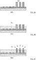
- EP 2936571 B1 discloses methods for locally removing SW from a Wiresea growth, as illustrated in figures 1A-1E .
- the Wiresea growth can typically be achieved using a stack 10 comprising a substrate 11, a two-dimensional nucleation layer 12 and a growth masking layer 13, also referred as SAG layer for "Selective Area Growth” layer.
- SW 21 are grown from the nucleation layer 12 through apertures in the SAG layer 13, forming a single SW array 20 regularly distributed on the stack 10 all over the wafer ( figure 1A ).
- a protective photoresist layer 30a is first deposited on the single SW array 20 ( figure 1B ).
- a patterning of the protective photoresist layer 30a is then performed by conventional lithography, to leave areas free of protective layer 30a ( figure 1C ).
- SW 21 are removed from these areas free of protective layer 30a using either a wet etching process, a dry etching process, or a mechanical action to break the SW.
- the present invention is intended to overcome at least partially some of the aforementioned drawbacks.
- an object of the present invention is a method for local removal of semiconductor wires which allows the effective removal of SW while maintaining the integrity of the underlying layer.
- Another object of the present invention is a method for local removal of semiconductor wires which reduces the roughness of areas where SW are removed.
- the invention provides a method for local removal of semiconductor wires comprising the following steps :
- This method is advantageously designed to achieve a single etching step of the exposed regions of the composite layer with a selectivity S semicon :S encaps around 1:1.
- the SW are etched at about the same etching rate as the encapsulation layer in the exposed regions.
- the top surface of the underlying growth masking layer is thus always protected during the etching step. It prevents any damages of the underlying layer.
- the stop of the etching step can be controlled precisely, so as to obtain a thin residual composite layer.
- the SW are effectively removed in the exposed regions, while the surface roughness of the exposed regions after etching is drastically decreased compared to prior art methods.
- the effective removal of the SW is thus not depending on the height of the SW to be removed.
- the SW to be removed often have height variations and an overetch step is then required in prior art process.
- Such an overetch step contributes to partial etching of the underlying layer.
- forming a composite layer prior to a single etching step of said composite layer prevents from an overetch of the SW, while ensuring effective removal of the SW.
- Further removal of the encapsulating material may be performed, so as to free the SW in the regions protected by the hard mask. In the exposed regions, removing the encapsulating material in the residual composite layer may result in regularly distributed small SW residues of controlled height.
- SW residues are suitable for further manufacturing steps such as forming a dielectric collar at the base of the SW, unlike the residues obtained randomly by other prior art methods.
- the method according to the invention is therefore simpler than known methods for local removal of SW. It is also more efficient to remove SW while protecting underlying layers.
- Another object of the present invention is a method for manufacturing of semiconductor wires-based light emitting diode (SW-LED) which comprises the method claimed above.
- the overall SW-LED manufacturing method is then cost effective.
- the thickness of the encapsulating layer is greater than or equal to the height of a highest semiconductor wire of the semiconductor wires.
- the composite layer is bulk.
- the stack of layers comprises a nucleation layer in between the substrate and the growth masking layer, said semiconductor wires being at least partially grown from the nucleation layer through the growth masking layer.
- the semiconductor-based material is a GaN-based material.
- the encapsulating material is chosen among SiO2, SiN, SiON, or a flowable oxide.
- the anisotropic etching is performed using a plasma comprising chlorinated species, preferably an argon/chlorine-based plasma.
- the semiconductor wires have an average height between 1 ⁇ m and 15 ⁇ m and an average diameter between 0.1 ⁇ m and 2 ⁇ m.
- the encapsulation layer is formed by spin coating.
- the encapsulation layer is deposited by a deposition technique among plasma-enhanced chemical vapor deposition (PECVD), sub-atmospheric chemical vapor deposition (SACVD), low pressure chemical vapor deposition (LPCVD).
- PECVD plasma-enhanced chemical vapor deposition
- SACVD sub-atmospheric chemical vapor deposition
- LPCVD low pressure chemical vapor deposition
- the composite layer is planarized before patterning the hard mask.
- the hard mask and the encapsulating material are removed after stopping the anisotropic etching of the composite layer, so as to leave regions without semiconductor wires in place of the residual composite layer, and regions with semiconductor wires in place of the composite layer.
- the local SW removal method is in particular dedicated to the manufacture of SW-based optoelectronic devices, in particular LEDs.
- a LED typically includes p- and n-doped regions in relation with an active region where the light is emitted.
- the relative arrangement of a third layer between a first layer and a second layer does not necessarily mean that the layers are in direct contact with each other, but means that the third layer is either in direct contact with the first and second layers or separated from each other by at least one other layer or at least one other element.
- a p-doping includes all doping by positive charge carriers regardless of the concentration of dopants.
- a p-doping can be defined as a p, p+ or p++ doping.
- an n-doping includes all doping by negative charge carriers regardless of the concentration of dopants.
- an n-doping can be defined as an n, n+ or n++ doping.
- a device, a substrate, a layer, a SW, "based" on a material M means a device, a substrate, a layer, a SW comprising this material M only or this material M and possibly other materials, for example alloying elements, impurities or doping elements.
- a gallium nitride (GaN) SW may include gallium nitride (GaN or i-GaN) and/or doped gallium nitride (p-GaN, n-GaN) and/or gallium-indium nitride (InGaN) and/or gallium-aluminium nitride (AIGaN).
- depth, height and thickness are taken perpendicularly to a basal plane of the substrate.
- thickness for a layer, height for a SW, and depth for an etching for example.
- a direction substantially normal to a plane means a direction with an angle of 90 ⁇ 10° to the plane.
- SEM scanning electron microscopy
- TEM transmission electron microscopy
- a cross-sectional observation at a contact pad may determine whether there are SW residues having about the same height at the base of said contact pad, and whether these SW residues originate from SW previously grown through a SAG layer.
- Another characteristic result of the method according to the invention is a preserved SAG layer surface.
- SW 21 are preferably grown on a planar stack 10 of layers 12, 13 which lie on a substrate 11.
- the substrate 11 may be made of silicon, GaN or sapphire.
- Each layer 12, 13 of the stack 10 extend in a basal plane and the stack 10 is formed in a direction normal to the basal plane ( Figure 2A ).
- the stack 10 may include a two-dimensional (2D) nucleation layer 12 overlaid by a growth masking layer hereafter referred as Selective Area Growth (SAG) layer 13.
- 2D two-dimensional
- SAG Selective Area Growth
- Both 2D nucleation layer 12 and SAG layer 13 are preferably directly in contact to each other.
- the 2D nucleation layer 12 may be made of (Al)(In)(Ga)N, or of tantalum, of tantalum nitride, of niobium, of niobium nitride, of titanium, of titanium nitride, of hafnium, of hafnium nitride, of boron, of boron nitride, of magnesium, of magnesium nitride, of tungsten, of tungsten nitride, or of a combination thereof.
- the 2D nucleation layer 12 may have a thickness in the range 5 nm to 50 nm, typically 25 nm.
- the SAG layer 13 may be made of SiN, SiO2, SiON, HfO2, HfN, Sc2O3, ScN, Mg2O3 or other dielectric materials.
- the SAG layer 13 may have a thickness in the range 20 nm to 200 nm, typically 100 nm.
- Holes or apertures are regularly distributed, for example in a pitch of 5 ⁇ m, but can be any pitch sizes between 100 nm to 100 ⁇ m throughout the SAG layer 13 so as to expose the underlying 2D nucleation layer 12.
- These holes have a diameter ranging from some tens of nanometers to some micrometers, for example about 0.5 ⁇ m.
- These holes are designed to assist a local growth of SW 21 from the nucleation layer 12.
- SW 21 can be grown by different growth techniques depending on the desired internal structure of the SW 21.
- the internal structure may be a longitudinal structure or a radial structure.
- SW 21 having the longitudinal structure can be grown by preferably by Molecular Beam Epitaxy (MBE) or by metal organic chemical vapour deposition (MOCVD) or remote plasma chemical vapour deposition (RP-CVD) or HVPE (Halide Vapor Phase Epitaxy or Hydride Vapour Phase Epitaxy).
- MBE Molecular Beam Epitaxy
- MOCVD metal organic chemical vapour deposition
- RP-CVD remote plasma chemical vapour deposition
- HVPE Hydrode Vapor Phase Epitaxy or Hydride Vapour Phase Epitaxy
- such a longitudinal structure may include p-GaN and n-GaN regions arranged according to the direction normal to the basal plane, with InGaN quantum wells in between.
- SW 21 having the radial structure can be grown by Metal-Organic Chemical Vapour Deposition (MOCVD), or by Metal-Organic Vapour Phase Epitaxy (MOVPE), or by Hydride Vapour Phase Epitaxy (HVPE), or by Molecular Beam Epitaxy (MBE).
- MOCVD Metal-Organic Chemical Vapour Deposition
- MOVPE Metal-Organic Vapour Phase Epitaxy
- HVPE Hydride Vapour Phase Epitaxy
- MBE Molecular Beam Epitaxy
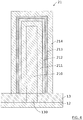
- such a radial structure may include p-GaN, InGaN and n-GaN regions concentrically arranged around an axis normal to the basal plane.
- Figure 4 shows a particular arrangement for such a radial structure.
- SW 21 can include the following sequence of regions or layers, from the inside to the outside of the SW in a radial direction:
- the core 210 of the SW 21 is first grown, for instance by MOCVD, through the holes 130 of the SAG layer 13. Then, layers 211, 212, 213, 214 may be successively grown on one another so as to form a radial structure, preferably as illustrated in figure 4 .
- SW 21 are illustrated in the following with a simple core-shell structure, regardless of the effective number of layers in the radial structure. It has also to be understood that this representation may also correspond to a longitudinal structure, if compatible.
- the single SW array 20 is first encapsulated 200 with an encapsulating material, as illustrated in figure 2B .
- the encapsulating material may be made of SiO2, SiON, SiN, BCB (Benzocyclobutene), poly methyl methacrylate (PMMA), or any form of epoxy, resin or dielectric materials.
- the encapsulating material may also be deposited by sub-atmospheric chemical vapor deposition (SACVD) or low pressure chemical vapor deposition (LPCVD).
- SACVD sub-atmospheric chemical vapor deposition
- LPCVD low pressure chemical vapor deposition
- the encapsulation layer 30b may be formed by spin-coating, for instance from a Flowable Oxide (FOx) or a spin-on glass, followed by annealing. These techniques are well known.
- FOx Flowable Oxide
- annealing annealing
- the thickness of the encapsulation layer 30b is preferably greater than or equal to the height of the semiconductor wires 21. In the case where SW 21 have different height to each other, the thickness of the encapsulation layer 30b is preferably greater than or equal to the highest SW 21.
- a composite layer 20b comprising both encapsulating material and semiconductor material is thus obtained.
- the composite layer 20b is preferably bulk, with no or few porosity within.
- the top surface of the composite layer 20b may be planarized, for instance by Chemical Mechanical Polishing (CMP), in order to get a flat top surface of the composite layer 20b.
- CMP Chemical Mechanical Polishing
- a low surface roughness preferably a peak-to-valley roughness lower than 100 nm, advantageously prevents over-etching during the subsequent etching of the composite layer 20b.
- a hard mask 40 is patterned 300 on the composite layer 20b, so as to protect regions of the composite layer 20b where SW 21 have to be kept and so as to expose regions of the composite layer 20b where SW 21 have to be removed ( figure 2C ).
- the regions of the composite layer 20b where SW 21 have to be removed may typically correspond to bonding pad regions and/or to chip trimming regions of LED.
- the regions of the composite layer 20b where SW 21 have to be kept may typically correspond to active regions of LED.
- a single etching step of the exposed regions of the composite layer 20b is then performed 400.
- Such a single etching step is preferably anisotropic and has a selectivity S semicon :S encaps between semiconductor-based material and encapsulating material such as 0.9:1 ⁇ S semicon :S encaps ⁇ 1.1:1.
- the selectivity S semicon :S encaps is preferably about 1:1 (one by one).
- the single etching step preferably consists in a dry etching performed by plasma, for instance by Reactive-Ion Etching (RIE).
- RIE Reactive-Ion Etching
- a Capacitively Coupled Plasma (CCP) reactor or an Inductively Coupled Plasma (ICP) reactor may be used.
- GaN-based SW 21 encapsulated in SiO2 a selectivity GaN:SiO2 about 1:1 may be obtained using an argon/chlorine-based plasma.
- a selectivity GaN:SiO2 about 1:1 may also be obtained using low pressure Cl2/BCl3 inductively coupled plasmas, as described in the document " S. Zhuo et al., Dry etching characteristics of GaN using Cl2/BCl3 inductively coupled plasmas, Applied Surface Science, 905-910 (2010 )".
- the anisotropic etching of the composite layer 20b is preferably performed so as to leave a thin residual composite layer 20c having a thickness h lower than 500 nm, and preferably lower than 200 nm ( figure 2D ).
- This thin residual composite layer 20c prevents over-etching.
- the underlying SAG layer 13 is thus protected.
- the encapsulating material can then be removed 500, for instance by wet etching, in order to free the SW 21 in the protected regions of the composite layer 20b, as illustrated in figure 2E .
- SiO2 or FOx encapsulating material this can be achieved using typically a wet chemistry solution based on hydrofluoric acid HF.
- a good selectivity etchant against the SAG layer is necessary, otherwise areas where SW have been etched will need to be patterned or masked to prevent parasitic SAG etching.
- SW residues 22 coming from the residual composite layer 20c may persist after such a wet etching. These SW residues 22 are substantially composed of the same layers as the SW 21 at their base.
- SW residues 22 all have about the same height h with h ⁇ 500 nm, and preferably h ⁇ 200 nm. Their diameters are close to the diameters of the SW 21 at their base.
- SW residues 22 it is important to have such a controlled height h in a reproducible way. Subsequent manufacturing steps can further be adjusted in accordance with the SW residues 22. The reproducibility of the overall manufacturing process is improved.
- figures 3A to 3E describe further steps typically involved in manufacturing SW-based LED.
- a conformal dielectric layer 50 may be deposited 501 ( figure 3A ).
- a masking layer 51 is then deposited 502, for instance by spin-coating, in order to protect a lower part of the SW 21 while exposing an upper part of the SW 21 ( figure 3B ).
- the thickness of the masking layer 51 is chosen in such a way that the upper part of the SW 21 is at least 500 nm high.
- An isotropic etching is then performed 503 in order to remove the exposed part of the dielectric layer 50 surrounding the upper part of the SW 21 ( figure 3C ).
- the masking layer 51 is then removed 504 ( figure 3D ).
- a dielectric collar 50a surrounding the lower part of the SW 21 is thus obtained, as well as a dielectric layer 50b covering the SW residues 22.
- Transparent Conductive Oxide (TCO) layer 52 and metallic pad contact 53 may then be deposited 505, so as to form a SW-based LED ( figure 3E ).
- the TCO and pad contact are thus isolated from the SW residues 22 and from the substrate 11, while connecting the exposed upper part of the SW 21.
Landscapes
- Led Devices (AREA)
Priority Applications (4)
| Application Number | Priority Date | Filing Date | Title |
|---|---|---|---|
| EP19315044.8A EP3754731A1 (fr) | 2019-06-21 | 2019-06-21 | Procédé d'enlèvement local de fils semi-conducteurs |
| US17/621,058 US20220336694A1 (en) | 2019-06-21 | 2020-06-19 | Method for local removal of semiconductor wires |
| PCT/EP2020/067078 WO2020254563A1 (fr) | 2019-06-21 | 2020-06-19 | Procédé d'élimination locale de fils semi-conducteurs |
| EP20732954.1A EP3987579A1 (fr) | 2019-06-21 | 2020-06-19 | Procédé d'élimination locale de fils semi-conducteurs |
Applications Claiming Priority (1)
| Application Number | Priority Date | Filing Date | Title |
|---|---|---|---|
| EP19315044.8A EP3754731A1 (fr) | 2019-06-21 | 2019-06-21 | Procédé d'enlèvement local de fils semi-conducteurs |
Publications (1)
| Publication Number | Publication Date |
|---|---|
| EP3754731A1 true EP3754731A1 (fr) | 2020-12-23 |
Family
ID=67482912
Family Applications (2)
| Application Number | Title | Priority Date | Filing Date |
|---|---|---|---|
| EP19315044.8A Withdrawn EP3754731A1 (fr) | 2019-06-21 | 2019-06-21 | Procédé d'enlèvement local de fils semi-conducteurs |
| EP20732954.1A Pending EP3987579A1 (fr) | 2019-06-21 | 2020-06-19 | Procédé d'élimination locale de fils semi-conducteurs |
Family Applications After (1)
| Application Number | Title | Priority Date | Filing Date |
|---|---|---|---|
| EP20732954.1A Pending EP3987579A1 (fr) | 2019-06-21 | 2020-06-19 | Procédé d'élimination locale de fils semi-conducteurs |
Country Status (3)
| Country | Link |
|---|---|
| US (1) | US20220336694A1 (fr) |
| EP (2) | EP3754731A1 (fr) |
| WO (1) | WO2020254563A1 (fr) |
Citations (4)
| Publication number | Priority date | Publication date | Assignee | Title |
|---|---|---|---|---|
| US20140370625A1 (en) * | 2013-06-18 | 2014-12-18 | Glo Ab | Stopping An Etch In A Planar Layer After Etching A 3D Structure |
| EP2936571A1 (fr) | 2012-12-21 | 2015-10-28 | Aledia | Processus de production de régions adjacentes comprenant des fils électriques de diode électroluminescente et dispositif obtenu à l'aide du processus |
| US20160064609A1 (en) * | 2014-08-29 | 2016-03-03 | Samsung Electronics Co., Ltd. | Nanostructure semiconductor light emitting device |
| US20180198047A1 (en) * | 2017-01-09 | 2018-07-12 | Glo Ab | Light emitting diodes with integrated reflector for a direct view display and method of making thereof |
Family Cites Families (8)
| Publication number | Priority date | Publication date | Assignee | Title |
|---|---|---|---|---|
| FR2951875B1 (fr) * | 2009-10-23 | 2012-05-18 | Commissariat Energie Atomique | Procede de fabrication d?un ecran a tres haute resolution utilisant une couche conductrice anisotropique et emissive |
| KR20150103661A (ko) * | 2012-10-26 | 2015-09-11 | 글로 에이비 | 나노와이어 led 구조 및 이를 제조하는 방법 |
| US9368672B2 (en) * | 2013-06-18 | 2016-06-14 | Glo Ab | Removal of 3D semiconductor structures by dry etching |
| US9571061B2 (en) * | 2014-06-06 | 2017-02-14 | Akoustis, Inc. | Integrated circuit configured with two or more single crystal acoustic resonator devices |
| WO2017111827A1 (fr) * | 2015-12-26 | 2017-06-29 | Intel Corporation | Pixel de del à nanofils |
| US10186630B2 (en) * | 2016-08-02 | 2019-01-22 | QMAT, Inc. | Seed wafer for GaN thickening using gas- or liquid-phase epitaxy |
| CN110709989B (zh) * | 2017-03-30 | 2023-12-01 | 维耶尔公司 | 垂直固态装置 |
| US12224304B2 (en) * | 2020-04-09 | 2025-02-11 | Raysolve Optoelectronics (Suzhou) Company Limited | Light emitting diode structure with individual fuctionable LED units and method for manufacturing the same |
-
2019
- 2019-06-21 EP EP19315044.8A patent/EP3754731A1/fr not_active Withdrawn
-
2020
- 2020-06-19 US US17/621,058 patent/US20220336694A1/en active Pending
- 2020-06-19 EP EP20732954.1A patent/EP3987579A1/fr active Pending
- 2020-06-19 WO PCT/EP2020/067078 patent/WO2020254563A1/fr not_active Ceased
Patent Citations (5)
| Publication number | Priority date | Publication date | Assignee | Title |
|---|---|---|---|---|
| EP2936571A1 (fr) | 2012-12-21 | 2015-10-28 | Aledia | Processus de production de régions adjacentes comprenant des fils électriques de diode électroluminescente et dispositif obtenu à l'aide du processus |
| US20150333216A1 (en) * | 2012-12-21 | 2015-11-19 | Aledia | Process for producing adjacent chips comprising led wires and device obtained by the process |
| US20140370625A1 (en) * | 2013-06-18 | 2014-12-18 | Glo Ab | Stopping An Etch In A Planar Layer After Etching A 3D Structure |
| US20160064609A1 (en) * | 2014-08-29 | 2016-03-03 | Samsung Electronics Co., Ltd. | Nanostructure semiconductor light emitting device |
| US20180198047A1 (en) * | 2017-01-09 | 2018-07-12 | Glo Ab | Light emitting diodes with integrated reflector for a direct view display and method of making thereof |
Non-Patent Citations (1)
| Title |
|---|
| S. ZHUO ET AL.: "Dry etching characteristics of GaN using CI2/BCI3 inductively coupled plasmas", APPLIED SURFACE SCIENCE, 2010, pages 905 - 910 |
Also Published As
| Publication number | Publication date |
|---|---|
| WO2020254563A1 (fr) | 2020-12-24 |
| US20220336694A1 (en) | 2022-10-20 |
| EP3987579A1 (fr) | 2022-04-27 |
Similar Documents
| Publication | Publication Date | Title |
|---|---|---|
| US9356191B2 (en) | Epitaxial layer wafer having void for separating growth substrate therefrom and semiconductor device fabricated using the same | |
| CN110291645B (zh) | 用于垂直型功率器件的方法和系统 | |
| JP7418583B2 (ja) | モノリシック発光ダイオード前駆体を形成する方法 | |
| US12300580B2 (en) | Semiconductor device and method | |
| EP2736068A2 (fr) | Procédé de recyclage de substrat et substrat recyclé | |
| EP3241246B1 (fr) | Procédé de fabrication de nanofils ou de microfils semiconducteurs à pieds isolés | |
| US20130175671A1 (en) | Methods for processing a semiconductor wafer, a semiconductor wafer and a semiconductor device | |
| EP2043157A1 (fr) | Diode à barrière schottky et procédé de fabrication de celle-ci | |
| US8357557B2 (en) | Semiconductor light-emitting device and process for production thereof | |
| WO2010108331A1 (fr) | Procédé de production de structures minces semi-conductrices | |
| EP3754731A1 (fr) | Procédé d'enlèvement local de fils semi-conducteurs | |
| US20090250748A1 (en) | Semiconductor device and method of fabricating the same | |
| US20240372319A1 (en) | Method of manufacturing a semiconductor device and semiconductor device | |
| US12490568B2 (en) | Method of forming a dielectric collar for semiconductor wires | |
| US6806204B1 (en) | Semiconductor etch speed modification | |
| US20210104645A1 (en) | Optoelectronic semiconductor component having a contact structure, and method for producing a contact structure for an optoelectronic semiconductor component | |
| US20240030381A1 (en) | Method for Producing a Semiconductor Body and Semicondcutor Arrangement | |
| US20150014824A1 (en) | Method for fabricating a semiconductor device | |
| US20230317772A1 (en) | Selective etching of silicon layers in a semiconductor device | |
| US20260114249A1 (en) | HEMT (High Electron Mobility Transistor) And Method Therefor | |
| US12159873B2 (en) | Semiconductor structure and manufacturing method thereof | |
| JP7806265B2 (ja) | 光電子デバイスを処理する方法及び光電子デバイス | |
| US20250048784A1 (en) | Method of processing an optoelectronic device and optoelectronic device | |
| US6707114B1 (en) | Semiconductor wafer arrangement of a semiconductor wafer | |
| WO2024049625A1 (fr) | Procédés de formation de dispositifs à semi-conducteur avec des structures d'isolation |
Legal Events
| Date | Code | Title | Description |
|---|---|---|---|
| STAA | Information on the status of an ep patent application or granted ep patent |
Free format text: STATUS: UNKNOWN |
|
| PUAI | Public reference made under article 153(3) epc to a published international application that has entered the european phase |
Free format text: ORIGINAL CODE: 0009012 |
|
| STAA | Information on the status of an ep patent application or granted ep patent |
Free format text: STATUS: THE APPLICATION HAS BEEN PUBLISHED |
|
| AK | Designated contracting states |
Kind code of ref document: A1 Designated state(s): AL AT BE BG CH CY CZ DE DK EE ES FI FR GB GR HR HU IE IS IT LI LT LU LV MC MK MT NL NO PL PT RO RS SE SI SK SM TR |
|
| AX | Request for extension of the european patent |
Extension state: BA ME |
|
| STAA | Information on the status of an ep patent application or granted ep patent |
Free format text: STATUS: THE APPLICATION IS DEEMED TO BE WITHDRAWN |
|
| 18D | Application deemed to be withdrawn |
Effective date: 20210624 |