EP3834227B1 - Ic-gehäuse - Google Patents
Ic-gehäuse Download PDFInfo
- Publication number
- EP3834227B1 EP3834227B1 EP18938731.9A EP18938731A EP3834227B1 EP 3834227 B1 EP3834227 B1 EP 3834227B1 EP 18938731 A EP18938731 A EP 18938731A EP 3834227 B1 EP3834227 B1 EP 3834227B1
- Authority
- EP
- European Patent Office
- Prior art keywords
- chips
- package
- marking plate
- plastic structure
- major surface
- Prior art date
- Legal status (The legal status is an assumption and is not a legal conclusion. Google has not performed a legal analysis and makes no representation as to the accuracy of the status listed.)
- Active
Links
Images



Classifications
-
- H—ELECTRICITY
- H10—SEMICONDUCTOR DEVICES; ELECTRIC SOLID-STATE DEVICES NOT OTHERWISE PROVIDED FOR
- H10W—GENERIC PACKAGES, INTERCONNECTIONS, CONNECTORS OR OTHER CONSTRUCTIONAL DETAILS OF DEVICES COVERED BY CLASS H10
- H10W40/00—Arrangements for thermal protection or thermal control
- H10W40/20—Arrangements for cooling
- H10W40/22—Arrangements for cooling characterised by their shape, e.g. having conical or cylindrical projections
-
- H—ELECTRICITY
- H10—SEMICONDUCTOR DEVICES; ELECTRIC SOLID-STATE DEVICES NOT OTHERWISE PROVIDED FOR
- H10W—GENERIC PACKAGES, INTERCONNECTIONS, CONNECTORS OR OTHER CONSTRUCTIONAL DETAILS OF DEVICES COVERED BY CLASS H10
- H10W40/00—Arrangements for thermal protection or thermal control
- H10W40/70—Fillings or auxiliary members in containers or in encapsulations for thermal protection or control
- H10W40/77—Auxiliary members characterised by their shape
- H10W40/778—Auxiliary members characterised by their shape in encapsulations
-
- H—ELECTRICITY
- H10—SEMICONDUCTOR DEVICES; ELECTRIC SOLID-STATE DEVICES NOT OTHERWISE PROVIDED FOR
- H10W—GENERIC PACKAGES, INTERCONNECTIONS, CONNECTORS OR OTHER CONSTRUCTIONAL DETAILS OF DEVICES COVERED BY CLASS H10
- H10W42/00—Arrangements for protection of devices
- H10W42/121—Arrangements for protection of devices protecting against mechanical damage
-
- H—ELECTRICITY
- H10—SEMICONDUCTOR DEVICES; ELECTRIC SOLID-STATE DEVICES NOT OTHERWISE PROVIDED FOR
- H10W—GENERIC PACKAGES, INTERCONNECTIONS, CONNECTORS OR OTHER CONSTRUCTIONAL DETAILS OF DEVICES COVERED BY CLASS H10
- H10W46/00—Marks applied to devices, e.g. for alignment or identification
-
- H—ELECTRICITY
- H10—SEMICONDUCTOR DEVICES; ELECTRIC SOLID-STATE DEVICES NOT OTHERWISE PROVIDED FOR
- H10W—GENERIC PACKAGES, INTERCONNECTIONS, CONNECTORS OR OTHER CONSTRUCTIONAL DETAILS OF DEVICES COVERED BY CLASS H10
- H10W72/00—Interconnections or connectors in packages
- H10W72/30—Die-attach connectors
-
- H—ELECTRICITY
- H10—SEMICONDUCTOR DEVICES; ELECTRIC SOLID-STATE DEVICES NOT OTHERWISE PROVIDED FOR
- H10W—GENERIC PACKAGES, INTERCONNECTIONS, CONNECTORS OR OTHER CONSTRUCTIONAL DETAILS OF DEVICES COVERED BY CLASS H10
- H10W72/00—Interconnections or connectors in packages
- H10W72/50—Bond wires
-
- H—ELECTRICITY
- H10—SEMICONDUCTOR DEVICES; ELECTRIC SOLID-STATE DEVICES NOT OTHERWISE PROVIDED FOR
- H10W—GENERIC PACKAGES, INTERCONNECTIONS, CONNECTORS OR OTHER CONSTRUCTIONAL DETAILS OF DEVICES COVERED BY CLASS H10
- H10W72/00—Interconnections or connectors in packages
- H10W72/851—Dispositions of multiple connectors or interconnections
-
- H—ELECTRICITY
- H10—SEMICONDUCTOR DEVICES; ELECTRIC SOLID-STATE DEVICES NOT OTHERWISE PROVIDED FOR
- H10W—GENERIC PACKAGES, INTERCONNECTIONS, CONNECTORS OR OTHER CONSTRUCTIONAL DETAILS OF DEVICES COVERED BY CLASS H10
- H10W74/00—Encapsulations, e.g. protective coatings
- H10W74/01—Manufacture or treatment
-
- H—ELECTRICITY
- H10—SEMICONDUCTOR DEVICES; ELECTRIC SOLID-STATE DEVICES NOT OTHERWISE PROVIDED FOR
- H10W—GENERIC PACKAGES, INTERCONNECTIONS, CONNECTORS OR OTHER CONSTRUCTIONAL DETAILS OF DEVICES COVERED BY CLASS H10
- H10W74/00—Encapsulations, e.g. protective coatings
- H10W74/01—Manufacture or treatment
- H10W74/019—Manufacture or treatment using temporary auxiliary substrates
-
- H—ELECTRICITY
- H10—SEMICONDUCTOR DEVICES; ELECTRIC SOLID-STATE DEVICES NOT OTHERWISE PROVIDED FOR
- H10W—GENERIC PACKAGES, INTERCONNECTIONS, CONNECTORS OR OTHER CONSTRUCTIONAL DETAILS OF DEVICES COVERED BY CLASS H10
- H10W74/00—Encapsulations, e.g. protective coatings
- H10W74/10—Encapsulations, e.g. protective coatings characterised by their shape or disposition
- H10W74/111—Encapsulations, e.g. protective coatings characterised by their shape or disposition the semiconductor body being completely enclosed
-
- H—ELECTRICITY
- H10—SEMICONDUCTOR DEVICES; ELECTRIC SOLID-STATE DEVICES NOT OTHERWISE PROVIDED FOR
- H10W—GENERIC PACKAGES, INTERCONNECTIONS, CONNECTORS OR OTHER CONSTRUCTIONAL DETAILS OF DEVICES COVERED BY CLASS H10
- H10W74/00—Encapsulations, e.g. protective coatings
- H10W74/10—Encapsulations, e.g. protective coatings characterised by their shape or disposition
- H10W74/111—Encapsulations, e.g. protective coatings characterised by their shape or disposition the semiconductor body being completely enclosed
- H10W74/114—Encapsulations, e.g. protective coatings characterised by their shape or disposition the semiconductor body being completely enclosed by a substrate and the encapsulations
- H10W74/117—Encapsulations, e.g. protective coatings characterised by their shape or disposition the semiconductor body being completely enclosed by a substrate and the encapsulations the substrate having spherical bumps for external connection
-
- H—ELECTRICITY
- H10—SEMICONDUCTOR DEVICES; ELECTRIC SOLID-STATE DEVICES NOT OTHERWISE PROVIDED FOR
- H10W—GENERIC PACKAGES, INTERCONNECTIONS, CONNECTORS OR OTHER CONSTRUCTIONAL DETAILS OF DEVICES COVERED BY CLASS H10
- H10W76/00—Containers; Fillings or auxiliary members therefor; Seals
- H10W76/40—Fillings or auxiliary members in containers, e.g. centering rings
-
- H—ELECTRICITY
- H10—SEMICONDUCTOR DEVICES; ELECTRIC SOLID-STATE DEVICES NOT OTHERWISE PROVIDED FOR
- H10W—GENERIC PACKAGES, INTERCONNECTIONS, CONNECTORS OR OTHER CONSTRUCTIONAL DETAILS OF DEVICES COVERED BY CLASS H10
- H10W90/00—Package configurations
-
- H—ELECTRICITY
- H10—SEMICONDUCTOR DEVICES; ELECTRIC SOLID-STATE DEVICES NOT OTHERWISE PROVIDED FOR
- H10W—GENERIC PACKAGES, INTERCONNECTIONS, CONNECTORS OR OTHER CONSTRUCTIONAL DETAILS OF DEVICES COVERED BY CLASS H10
- H10W99/00—Subject matter not provided for in other groups of this subclass
-
- H—ELECTRICITY
- H10—SEMICONDUCTOR DEVICES; ELECTRIC SOLID-STATE DEVICES NOT OTHERWISE PROVIDED FOR
- H10W—GENERIC PACKAGES, INTERCONNECTIONS, CONNECTORS OR OTHER CONSTRUCTIONAL DETAILS OF DEVICES COVERED BY CLASS H10
- H10W46/00—Marks applied to devices, e.g. for alignment or identification
- H10W46/401—Marks applied to devices, e.g. for alignment or identification for identification or tracking
-
- H—ELECTRICITY
- H10—SEMICONDUCTOR DEVICES; ELECTRIC SOLID-STATE DEVICES NOT OTHERWISE PROVIDED FOR
- H10W—GENERIC PACKAGES, INTERCONNECTIONS, CONNECTORS OR OTHER CONSTRUCTIONAL DETAILS OF DEVICES COVERED BY CLASS H10
- H10W46/00—Marks applied to devices, e.g. for alignment or identification
- H10W46/601—Marks applied to devices, e.g. for alignment or identification for use after dicing
- H10W46/607—Located on parts of packages, e.g. on encapsulations or on package substrates
-
- H—ELECTRICITY
- H10—SEMICONDUCTOR DEVICES; ELECTRIC SOLID-STATE DEVICES NOT OTHERWISE PROVIDED FOR
- H10W—GENERIC PACKAGES, INTERCONNECTIONS, CONNECTORS OR OTHER CONSTRUCTIONAL DETAILS OF DEVICES COVERED BY CLASS H10
- H10W72/00—Interconnections or connectors in packages
- H10W72/071—Connecting or disconnecting
- H10W72/073—Connecting or disconnecting of die-attach connectors
-
- H—ELECTRICITY
- H10—SEMICONDUCTOR DEVICES; ELECTRIC SOLID-STATE DEVICES NOT OTHERWISE PROVIDED FOR
- H10W—GENERIC PACKAGES, INTERCONNECTIONS, CONNECTORS OR OTHER CONSTRUCTIONAL DETAILS OF DEVICES COVERED BY CLASS H10
- H10W72/00—Interconnections or connectors in packages
- H10W72/071—Connecting or disconnecting
- H10W72/075—Connecting or disconnecting of bond wires
-
- H—ELECTRICITY
- H10—SEMICONDUCTOR DEVICES; ELECTRIC SOLID-STATE DEVICES NOT OTHERWISE PROVIDED FOR
- H10W—GENERIC PACKAGES, INTERCONNECTIONS, CONNECTORS OR OTHER CONSTRUCTIONAL DETAILS OF DEVICES COVERED BY CLASS H10
- H10W72/00—Interconnections or connectors in packages
- H10W72/851—Dispositions of multiple connectors or interconnections
- H10W72/853—On the same surface
- H10W72/865—Die-attach connectors and bond wires
-
- H—ELECTRICITY
- H10—SEMICONDUCTOR DEVICES; ELECTRIC SOLID-STATE DEVICES NOT OTHERWISE PROVIDED FOR
- H10W—GENERIC PACKAGES, INTERCONNECTIONS, CONNECTORS OR OTHER CONSTRUCTIONAL DETAILS OF DEVICES COVERED BY CLASS H10
- H10W72/00—Interconnections or connectors in packages
- H10W72/851—Dispositions of multiple connectors or interconnections
- H10W72/874—On different surfaces
- H10W72/884—Die-attach connectors and bond wires
-
- H—ELECTRICITY
- H10—SEMICONDUCTOR DEVICES; ELECTRIC SOLID-STATE DEVICES NOT OTHERWISE PROVIDED FOR
- H10W—GENERIC PACKAGES, INTERCONNECTIONS, CONNECTORS OR OTHER CONSTRUCTIONAL DETAILS OF DEVICES COVERED BY CLASS H10
- H10W90/00—Package configurations
- H10W90/20—Configurations of stacked chips
- H10W90/24—Configurations of stacked chips at least one of the stacked chips being laterally offset from a neighbouring stacked chip, e.g. chip stacks having a staircase shape
-
- H—ELECTRICITY
- H10—SEMICONDUCTOR DEVICES; ELECTRIC SOLID-STATE DEVICES NOT OTHERWISE PROVIDED FOR
- H10W—GENERIC PACKAGES, INTERCONNECTIONS, CONNECTORS OR OTHER CONSTRUCTIONAL DETAILS OF DEVICES COVERED BY CLASS H10
- H10W90/00—Package configurations
- H10W90/701—Package configurations characterised by the relative positions of pads or connectors relative to package parts
- H10W90/731—Package configurations characterised by the relative positions of pads or connectors relative to package parts of die-attach connectors
- H10W90/732—Package configurations characterised by the relative positions of pads or connectors relative to package parts of die-attach connectors between stacked chips
-
- H—ELECTRICITY
- H10—SEMICONDUCTOR DEVICES; ELECTRIC SOLID-STATE DEVICES NOT OTHERWISE PROVIDED FOR
- H10W—GENERIC PACKAGES, INTERCONNECTIONS, CONNECTORS OR OTHER CONSTRUCTIONAL DETAILS OF DEVICES COVERED BY CLASS H10
- H10W90/00—Package configurations
- H10W90/701—Package configurations characterised by the relative positions of pads or connectors relative to package parts
- H10W90/731—Package configurations characterised by the relative positions of pads or connectors relative to package parts of die-attach connectors
- H10W90/734—Package configurations characterised by the relative positions of pads or connectors relative to package parts of die-attach connectors between a chip and a stacked insulating package substrate, interposer or RDL
-
- H—ELECTRICITY
- H10—SEMICONDUCTOR DEVICES; ELECTRIC SOLID-STATE DEVICES NOT OTHERWISE PROVIDED FOR
- H10W—GENERIC PACKAGES, INTERCONNECTIONS, CONNECTORS OR OTHER CONSTRUCTIONAL DETAILS OF DEVICES COVERED BY CLASS H10
- H10W90/00—Package configurations
- H10W90/701—Package configurations characterised by the relative positions of pads or connectors relative to package parts
- H10W90/731—Package configurations characterised by the relative positions of pads or connectors relative to package parts of die-attach connectors
- H10W90/736—Package configurations characterised by the relative positions of pads or connectors relative to package parts of die-attach connectors between a chip and a stacked lead frame, conducting package substrate or heat sink
-
- H—ELECTRICITY
- H10—SEMICONDUCTOR DEVICES; ELECTRIC SOLID-STATE DEVICES NOT OTHERWISE PROVIDED FOR
- H10W—GENERIC PACKAGES, INTERCONNECTIONS, CONNECTORS OR OTHER CONSTRUCTIONAL DETAILS OF DEVICES COVERED BY CLASS H10
- H10W90/00—Package configurations
- H10W90/701—Package configurations characterised by the relative positions of pads or connectors relative to package parts
- H10W90/751—Package configurations characterised by the relative positions of pads or connectors relative to package parts of bond wires
- H10W90/754—Package configurations characterised by the relative positions of pads or connectors relative to package parts of bond wires between a chip and a stacked insulating package substrate, interposer or RDL
-
- H—ELECTRICITY
- H10—SEMICONDUCTOR DEVICES; ELECTRIC SOLID-STATE DEVICES NOT OTHERWISE PROVIDED FOR
- H10W—GENERIC PACKAGES, INTERCONNECTIONS, CONNECTORS OR OTHER CONSTRUCTIONAL DETAILS OF DEVICES COVERED BY CLASS H10
- H10W90/00—Package configurations
- H10W90/701—Package configurations characterised by the relative positions of pads or connectors relative to package parts
- H10W90/751—Package configurations characterised by the relative positions of pads or connectors relative to package parts of bond wires
- H10W90/756—Package configurations characterised by the relative positions of pads or connectors relative to package parts of bond wires between a chip and a stacked lead frame, conducting package substrate or heat sink
Definitions
- integrated circuit (IC) packaging is a step in the semiconductor device fabrication that encapsulates one or more semiconductor dies (also referred to as IC chips) of integrated circuits in a supporting case that prevents physical damage, corrosion and the like.
- the supporting case with the encapsulated semiconductor die(s) is referred to as an IC package.
- the IC package can be laser-marked for identification and traceability.
- An integrated circuit (IC) package comprising a package substrate, one or more IC chips that are interconnected with the package substrate, a metal or metal alloy plate, the plate having a first major surface and a second major surface, while the marking plate being stacked on the one or more IC chips with the first major surface facing the one or more IC chips is in general disclosed in US 2016/005682 A1 and in US 2006/113663 A1 .
- An integrated circuit (IC) package as described above further comprising a plastic structure configured to encapsulate the one or more IC chips and the plate is described in US 2014/015148 A1 .
- US 2016/005696 A1 discloses a silicon marking plate, i.e.
- US 2006/231944 A1 discloses a marking plate in an IC package, the marking plate having a stair structure, but is silent on the marking plate having an equal coefficient of thermal expansion as the one or more IC chips.
- US 2009/001561 A1 discloses laser marking on the surface of a heat sink exposed at the package surface.
- the marking plate is formed of at least one of a ceramic material, a metal material, a metal alloy material In an embodiment, the marking plate is formed of a semiconductor material.
- the IC package includes a plurality of bond wires that are configured to interconnect the one or more IC chips to the package substrate.
- the plastic structure is configured to encapsulate the plurality of bond wires.
- the IC package is one of a ball grid array (BGA) package, a quad-flat package (QFP), a quad flat non-lead (QFN) package, a land grid array (LGA) package, and a pin grid array (PGA).
- BGA ball grid array
- QFP quad-flat package
- QFN quad flat non-lead
- LGA land grid array
- PGA pin grid array
- neighboring IC chips are staggered and multiple IC chips in the IC package are stacked in a zig-zag pattern.
- the marking plate has a better anti-laser penetration property than the plastic structure.
- the marking plate has a higher rigidity than the plastic structure.
- the marking plate has a better thermal conductivity than the plastic structure.
- first and second features are formed in direct contact
- additional features may be formed between the first and second features, such that the first and second features may not be in direct contact
- present disclosure may repeat reference numerals and/or letters in the various examples. This repetition is for the purpose of simplicity and clarity and does not in itself dictate a relationship between the various embodiments and/or configurations discussed.
- spatially relative terms such as “beneath,” “below,” “lower,” “above,” “upper” and the like, may be used herein for ease of description to describe one element or feature's relationship to another element(s) or feature(s) as illustrated in the figures.
- the spatially relative terms are intended to encompass different orientations of the device in use or operation in addition to the orientation depicted in the figures.
- the apparatus may be otherwise oriented (rotated 90 degrees or at other orientations) and the spatially relative descriptors used herein may likewise be interpreted accordingly.
- aspects of the disclosure provide an integrated circuit(IC) package with a marking plate embedded in a plastic structure.
- the marking plate has a higher rigidity than the molding material of the plastic structure, and has a better anti-laser penetration property than the molding material. Because of the higher rigidity, the IC package distortion due to high temperature processing, such as a soldering process, can be reduced. Further, because of the better anti-laser penetration property, a relatively thinner marking plate is allowed. Thus, the IC package can have a relatively small thickness or can encapsulate more IC chips without increasing the package thickness.
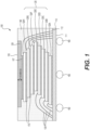
- Fig. 1 shows a cross-sectional view of an integrated circuit (IC) package 100 in accordance with some embodiments.
- the IC package 100 includes a package substrate 110, a plurality of IC chips 120 (e.g., including IC chips 120A-120H in Fig. 1 ) and a marking plate 150.
- the IC chips 120 are stacked on the package substrate 110 and are encapsulated in a plastic structure 140.
- the marking plate 150 is stacked on the IC chips 120 and is embedded in the plastic structure 140.
- a surface 155 of the marking plate 150 is a portion of the outer surface of the IC package 100 and the surface 155 can be laser-marked for identification and traceability.
- the package substrate 110 is made, for example, of suitable insulating material (also referred to as dielectric material), such as an epoxy based laminate substrate, a resin-based Bismaleimide-Triazine (BT) substrate, and the like.
- the package substrate 110 is relatively rigid to provide mechanical support to the IC chips 120.
- the package substrate 110 has a first surface 111 and a second surface 112.
- the IC chips 120 are disposed on a surface, such as the second surface 112 of the package substrate 110.
- the package substrate 110 also provides electrical support for the IC chips 120.
- the package substrate 110 includes multiple layers of metal traces, such as copper wires, and the like with the insulating material in between. The metal traces on the different layers can be connected by vias. Further, contact structures are formed on both the first surface 111 and the second surface 112 to electrically interface the IC chips 120 in the IC package 100 to components out of the IC package 100.
- the IC chips 120 can be any suitable chips.
- the IC chips 120 include various circuits for providing storage, computing and/or processing functionalities.
- the package substrate 110 provides interconnects from the inputs/outputs of the IC chips 120 to the contact structures that are formed on the first surface 111 and the second surface 112 of the IC package 100.
- the IC chips 120 includes input/output (I/O) pads (not shown) that are electrically connected to internal circuits that are formed on the IC chips 120.
- Bond wires 130 e.g. aluminum wires, copper wires, silver wires, gold wires and the like
- neighboring IC chips in the IC chips 120 are staggered to provide bonding space to allow the bond wires 130 to be bonded on the I/O pads, and avoid shorting circuit. Further, the IC chips 120 are stacked in a zig-zag pattern to provide space for bond wires 130.
- the package substrate 110 also includes suitable contact structures 160 on the first surface 111.
- the IC package 100 is a ball grid array (BGA) package, and each of the contact structures 160 includes a solder pad and a solder ball that is deposited on the solder pad. It is noted that, in some examples, the solder balls are not formed on the package substrate 110.
- the IC package is a quad-flat package (QFP).
- the IC package 100 is a quad flat non-lead (QFN) package.
- the IC package 100 is a land grid array (LGA) package, and each of the contact structures includes a solder pad.
- the IC package 100 is a pin grid array (PGA) package, and each of the contact structures 160 includes a pin.
- the package substrate 110, the plastic structure 140 and the marking plate 150 form the outer portion of the IC package 100 that encapsulates the IC chips 120 inside.
- the marking plate 150 is stacked on the IC chips 120.
- the second surface 112 of the package substrate 110, the IC chips 120 and the bond wires 130 are encapsulated by the plastic structure 140.
- the marking plate 150 is embedded in the plastic structure 140 with the surface 155 exposed for laser-marking.
- the plastic structure 140 is formed of any suitable material, such as silica fillers, resin, and the like.
- the plastic structure 140 includes epoxy molding compound (EMC).
- EMC epoxy molding compound
- the plastic structure 140 and IC chips 120 have different coefficient thermal expansions (CTE) (also referred to as CTE mismatch), and have different thermal conductivity.
- CTE coefficient thermal expansions
- the marking plate 150 is formed of a material that has a higher rigidity than the plastic structure 140.
- the IC package 100 includes the marking plate 150, the IC chips 120 and the package substrate 110 from the upper surface (e.g., the surface 155 of the marking plate 150) to the bottom surface (e.g., the first surface 111 of the package substrate 110).
- the marking plate 150, the IC chips and the package substrate 110 have relatively high rigidity than the plastic structure 140.
- the upper portion of a related IC package is also made of EMC, and is used for laser-marking. Compared to the conventional example, the IC package 100 has lower volume percentage of EMC, and thus has higher package rigidity than the conventional example.
- the marking plate 150 has about the same CTE (e.g., matching CTE) as the IC chips 120.
- the IC package 110 has a reduced warpage during thermal processing.
- CTE mismatch can cause package warpage during thermal processing after molding.
- the IC packages can be mounted on a printed circuit board (PCB) using a surface mount process.
- the surface mount process includes a solder reflow step that raises a processing temperature, for example, above 200°C. When the processing temperature returns to for example room temperature, the IC package 100 has reduced warpage compared to the conventional example due to the matching CTE from the upper surface to the bottom surface.
- the marking plate 150 has a better anti-laser penetration property than the plastic structure 140 to prevent laser penetration.
- a laser penetration depth in the marking plate 150 is shorter than a laser penetration depth in the plastic structure 140.
- the IC package 100 has a reduced thickness or can include more IC chips 120.
- the top portion of the plastic package above the IC chips needs to be relatively thick, such as about 150 ⁇ m.
- the marking plate 150 has a better anti-laser penetration property than the plastic structure 140, and a thickness of 30 ⁇ m is enough to prevent laser damage to the circuits on the IC chips 120 and the bond wires 130.
- the marking plate 150 has a better thermal conductivity than the plastic structure 140.
- the marking plate 150 can transfer heat generated by the IC chips during operation to the outer surface of the IC package 100 faster than the plastic structure 140.
- the fast heat transfer can provide proper thermal environment for the IC chips 120, reduce chip temperature during operation, and allow the IC chips 120 to perform properly during operation.
- the marking plate 150 is formed of silicon, such as pure silicon, and is then referred to as a mirror die (due to shining surface 155) in an example.
- the marking plate 150 has about the same CTE (e.g., matching CTE) as the IC chips 120, and has a higher rigidity and better anti-laser penetration property than the plastic structure 140.
- the marking plate 150 is formed of ceramic material. In another example, the marking plate 150 is formed of metal alloy.
- the marking plate 150 is suitably processed such that the bottom surface of the marking plate 150 that faces the IC chips 120 is electrically non-conductive to avoid shorting to the bond wires 130.
- the marking plate 150 is configured to have a stair shape at the cross-sectional view.
- the surface 157 of the marking plate 150 that faces the IC chip 120H is smaller than the surface 155 of the marking plate 150.
- the smaller surface 157 provides more space for wire-bonding on the IC chip 120H.
- the larger surface 155 allows more area for laser markings.
- IC chips 120 are shown with the same chip size in Fig. 1 , the IC chips 120 can have different chip sizes in other examples.
- intermediate layers 170 such as adhesive films, polymer films, spacer films, and the like can be used between the IC chips 120 and the marking plate 150.
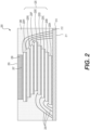
- Fig. 2 shows a cross-sectional view of another IC package 200 in accordance with some examples, not being part of the invention.
- the IC package 200 includes a package substrate 210, a plurality of IC chips 220 and a marking plate 250.
- the IC chips 220 are stacked on the package substrate 210 and are encapsulated in a plastic structure 240.
- the marking plate 250 is stacked on the IC chips 220 and is embedded in the plastic structure 240.
- a surface 255 of the marking plate 250 is a portion of the outer surface of the IC package 200 and the surface 255 can be laser-marked for identification and traceability.
- the IC package 200 utilizes certain components that are identical, equivalent or similar to those used in the IC package 100.
- the IC chips 220 are equivalent or similar to the IC chips 120.
- the bond wires 230 are equivalent or similar to the bond wires 130.
- the plastic structure 240 is equivalent or similar to the plastic structure 140.
- the package substrate 210 is equivalent or similar to the package substrate 110. The description of these components has been provided above and will be omitted here for clarity purposes.
- the marking plate 250 is configured to have a rectangular cuboid shape, and have a rectangular shape in the cross-sectional view, thus the surface 257 that faces the IC chip 220H is of the same surface area as the surface 255 that is a portion of the outer surface of the IC package 200.
- the IC package 200 can be a LGA package without soldering balls.
- the package substrate 210 includes flat contact structures on the first surface 211.
- Fig. 3 shows a flow chart outlining a process 300 for fabrication according some embodiments of the disclosure.
- the process 300 is used to fabricate the IC package 100.
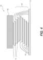
- Figs. 4-6 show various cross sectional views of the IC package 100 at intermediate stages during the process 300 in accordance with some embodiments. It is noted that suitable modifications can be made on the Figs. 4-6 for other IC package, such as the IC package 200.
- IC chips are stacked on a package substrate.
- the plurality of IC chips 120 are stacked on the package substrate 110.
- the IC chips 120 are stacked in a staggered manner to provide more space for wire bonding.
- neighboring IC chips in the IC chips 120 area staggered to provide space for wire bonding.
- the IC chips 120 can be stacked in a zig-zag pattern.
- bond wires 130 are bonded to interconnect the IC chips 120 to the package substrate 110.
- adhesive films 170 are used between the neighboring IC chips 120.
- an initial marking plate is stacked on the IC chips.
- an initial marking plate 450 is stacked on the IC chips 120. It is noted that the initial marking plate 450 is thicker than the marking plate 150 in the IC package 100.
- an adhesive film 170 is used between the initial marking plate 450 and the top of IC chips 120.
- the initial marking plate and the IC chips are encapsulated in an initial plastic structure.
- plastic material such as EMC and the like is molded to form the initial plastic structure 540 that encapsulates the IC chips 120 and the initial marking plate 450.
- the initial plastic structure is grinded. As shown in Fig. 5 , the initial plastic structure 540 is grinded to expose the initial marking plate 450, and further grinded to form the plastic structure 140 and the marking plate 150. Fig. 6 shows the IC package after the grinding process.
- the IC package is laser marked on the marking plate.
- laser marking can be performed on the marking plate 150 for identification and traceability.
- solder balls such as the solder balls 160 are attached to the package substrate 110.
- the IC packaging is performed in the form of a matrix array of packages. The matrix array of packages can be diced to form individual IC packages. The individual IC packages can then be tested and sorted. Then, the process proceeds to S399 and terminates.
Landscapes
- Structures Or Materials For Encapsulating Or Coating Semiconductor Devices Or Solid State Devices (AREA)
- Engineering & Computer Science (AREA)
- Manufacturing & Machinery (AREA)
- Laser Beam Processing (AREA)
Claims (11)
- Gehäuse für integrierte Schaltungen, IC-Gehäuse,(100), umfassend:ein Gehäusesubstrat (110);einen oder mehrere IC-Chips (120), die mit dem Gehäusesubstrat (110) verbunden sind;eine Markierungsplatte (150), die für eine Lasermarkierung geeignet ist oder lasermarkiert ist, mit einer ersten Hauptfläche und einer zweiten Hauptfläche, wobei die Markierungsplatte (150) mit der dem einen oder den mehreren IC-Chips zugewandten Hauptfläche auf dem einen oder den mehreren IC-Chips (120) gestapelt ist und wobei die Markierungsplatte eine Treppenstruktur aufweist;eine Kunststoffstruktur (140), die ausgebildet ist zum Einkapseln des einen oder der mehreren IC-Chips (120) und der Markierungsplatte (150), wobei die zweite Hauptfläche der Markierungsplatte (150) ein Teil einer Außenfläche des IC-Gehäuses (120) ist, wobeieine Lasereindringtiefe in die Markierungsplatte kürzer ist als eine Lasereindringtiefe in die Kunststoffstruktur (140) und wobeidie erste Hauptfläche der Markierungsplatte kleiner ist als die zweite Hauptfläche der Markierungsplatte,dadurch gekennzeichnet, dass die Markierungsplatte (150) einen gleichen Wärmeausdehnungskoeffizienten, CTE, wie der eine oder die mehreren IC-Chips (120) aufweist.
- IC-Gehäuse (100) nach Anspruch 1, wobei die Markierungsplatte (150) aus einem Halbleitermaterial gebildet ist.
- IC-Gehäuse (100) nach Anspruch 1, wobei eine Mehrzahl von Bonddrähten (130) ausgebildet ist zum Verbinden des einen oder der mehreren IC-Chips (120) mit dem Gehäusesubstrat (110); und die Kunststoffstruktur (140) ausgebildet ist zum Einkapseln der mehreren Bonddrähte (130).
- IC-Gehäuse (100) nach Anspruch 1, wobei das IC-Gehäuse eines der folgenden Gehäuse ist: ein Ball Grid Array, BGA, Package, ein Quad Flat Package, QFP, ein Quad Flat No Leads, QFN, Package, ein Land Grid Array, LGA, Package und ein Pin Grid Array, PGA, Package.
- IC-Gehäuse (100) nach Anspruch 1, wobei die benachbarten IC-Chips in dem einen oder den mehreren IC-Chips gestaffelt sind, um Raum für die Bonddrähte zu schaffen.
- IC-Gehäuse (100) nach Anspruch 1, wobei die Markierungsplatte (150) eine höhere Festigkeit aufweist als die Kunststoffstruktur (140).
- Verfahren zur Herstellung eines Gehäuses für integrierte Schaltungen, IC-Gehäuse, (100), umfassend:Stapeln eines oder mehrerer IC-Chips (120) auf einem Gehäusesubstrat (110);Bilden einer Markierungsplatte (150) auf dem einen oder den mehreren IC-Chips (120), wobei eine erste Hauptfläche dem einen oder den mehreren IC-Chips (120) zugewandt ist und wobei die Markierungsplatte (150) eine Treppenstruktur aufweist; undBilden einer Kunststoffstruktur (140), die den einen oder die mehreren IC-Chips (120) und die Markierungsplatte (150) einkapselt, wobei eine zweite Hauptfläche der Markierungsplatte (150) ein Teil einer Außenfläche des IC-Gehäuses (100) ist; undLasermarkieren auf der zweiten Hauptfläche der Markierungsplatte (150), wobeieine Lasereindringtiefe in die Markierungsplatte kürzer ist als eine Lasereindringtiefe in die Kunststoffstruktur (140) und wobeidas Bilden der Markierungsplatte (150) auf dem einen oder den mehreren IC-Chips (120) ferner umfasst:
Ausbilden der Markierungsplatte (150) mit der ersten Hauptfläche, die kleiner ist als die zweite Hauptfläche, dadurch gekennzeichnet, dass die Markierungsplatte (150) einen gleichen Wärmeausdehnungskoeffizienten, CTE, wie der eine oder die mehreren IC-Chips (120) aufweist. - Verfahren nach Anspruch 7, wobei das Bilden der Markierungsplatte (150) und der Kunststoffstruktur (140) ferner umfasst:Einkapseln einer Ausgangsmarkierungsplatte (450) und des einen oder der mehreren IC-Chips (120) in einer Ausgangskunststoffstruktur (540); undSchleifen der Ausgangskunststoffstruktur (540) und der Ausgangsmarkierungsplatte (450) zur Freilegung der zweiten Hauptfläche der Markierungsplatte (150).
- Verfahren nach Anspruch 7, ferner umfassend:Bereitstellen von Bonddrähten zur Verbindung des einen oder der mehreren IC-Chips (120) mit dem Gehäusesubstrat (110); wobeidas Bilden der k(110) das Einkapseln der gebondeten Drähte (130) umfasst.
- Verfahren nach Anspruch 7, wobei das Stapeln des einen oder der mehreren IC-Chips (120) auf dem Gehäusesubstrat (110) ferner umfasst:
Staffeln von benachbarten IC-Chips (120) in dem einen oder den mehreren IC-Chips, um Raum für die Bonddrähte (130) zu schaffen. - Verfahren nach Anspruch 7, wobei:
die Markierungsplatte (150) eine höhere Festigkeit aufweist als die Kunststoffstruktur (140).
Applications Claiming Priority (1)
| Application Number | Priority Date | Filing Date | Title |
|---|---|---|---|
| PCT/CN2018/112567 WO2020087253A1 (en) | 2018-10-30 | 2018-10-30 | Ic package |
Publications (3)
| Publication Number | Publication Date |
|---|---|
| EP3834227A1 EP3834227A1 (de) | 2021-06-16 |
| EP3834227A4 EP3834227A4 (de) | 2022-03-30 |
| EP3834227B1 true EP3834227B1 (de) | 2024-09-04 |
Family
ID=65872658
Family Applications (1)
| Application Number | Title | Priority Date | Filing Date |
|---|---|---|---|
| EP18938731.9A Active EP3834227B1 (de) | 2018-10-30 | 2018-10-30 | Ic-gehäuse |
Country Status (7)
| Country | Link |
|---|---|
| US (2) | US20200135656A1 (de) |
| EP (1) | EP3834227B1 (de) |
| JP (1) | JP7303294B2 (de) |
| KR (1) | KR20210033010A (de) |
| CN (1) | CN109564905A (de) |
| TW (1) | TWI754785B (de) |
| WO (1) | WO2020087253A1 (de) |
Families Citing this family (9)
| Publication number | Priority date | Publication date | Assignee | Title |
|---|---|---|---|---|
| KR102767617B1 (ko) * | 2019-08-12 | 2025-02-17 | 에스케이하이닉스 주식회사 | 적층 반도체 칩을 포함하는 반도체 패키지 |
| KR102904560B1 (ko) * | 2020-08-19 | 2025-12-26 | 에스케이하이닉스 주식회사 | 수직 인터커넥터를 포함하는 반도체 패키지 |
| KR102903837B1 (ko) | 2020-11-23 | 2025-12-24 | 삼성전자주식회사 | 반도체 패키지 |
| JP2023031660A (ja) * | 2021-08-25 | 2023-03-09 | キオクシア株式会社 | 半導体装置及び電子機器 |
| KR20230059877A (ko) | 2021-10-25 | 2023-05-04 | 삼성전자주식회사 | 반도체 패키지 및 그 제조 방법 |
| US20250006574A1 (en) * | 2021-11-05 | 2025-01-02 | Resonac Corporation | Reinforced semiconductor chip production method, semiconductor chip with film, semiconductor chip reinforcement method, reinforcement film and semiconductor device |
| CN114361115B (zh) * | 2021-12-31 | 2022-08-23 | 中山市木林森微电子有限公司 | 一种多芯片埋入式封装模块结构 |
| EP4270476A1 (de) * | 2022-04-29 | 2023-11-01 | Infineon Technologies Austria AG | Halbleitergehäuse und verfahren zum markieren eines halbleitergehäuses |
| KR20240102542A (ko) * | 2022-12-26 | 2024-07-03 | 삼성전자주식회사 | 보강 구조물을 포함하는 반도체 패키지 |
Citations (3)
| Publication number | Priority date | Publication date | Assignee | Title |
|---|---|---|---|---|
| JP3904934B2 (ja) * | 2002-01-29 | 2007-04-11 | 京セラ株式会社 | 半導体装置 |
| US20090001561A1 (en) * | 2006-12-21 | 2009-01-01 | Kok Hua Chua | High Thermal Performance Packaging for Circuit Dies |
| US20160005696A1 (en) * | 2013-02-21 | 2016-01-07 | Atsushi Tomohiro | Semiconductor device and method for manufacturing same |
Family Cites Families (40)
| Publication number | Priority date | Publication date | Assignee | Title |
|---|---|---|---|---|
| US4788627A (en) * | 1986-06-06 | 1988-11-29 | Tektronix, Inc. | Heat sink device using composite metal alloy |
| JPH0563113A (ja) * | 1991-09-04 | 1993-03-12 | Sony Corp | 樹脂封止型半導体装置 |
| US5461257A (en) * | 1994-03-31 | 1995-10-24 | Sgs-Thomson Microelectronics, Inc. | Integrated circuit package with flat-topped heat sink |
| US6238954B1 (en) * | 1999-09-28 | 2001-05-29 | Intel Corporation | COF packaged semiconductor |
| TW452956B (en) * | 2000-01-04 | 2001-09-01 | Siliconware Precision Industries Co Ltd | Heat dissipation structure of BGA semiconductor package |
| US6559525B2 (en) * | 2000-01-13 | 2003-05-06 | Siliconware Precision Industries Co., Ltd. | Semiconductor package having heat sink at the outer surface |
| JP2001217340A (ja) * | 2000-02-01 | 2001-08-10 | Nec Corp | 半導体装置及びその製造方法 |
| US6906414B2 (en) * | 2000-12-22 | 2005-06-14 | Broadcom Corporation | Ball grid array package with patterned stiffener layer |
| TW563212B (en) * | 2002-10-24 | 2003-11-21 | Advanced Semiconductor Eng | Semiconductor package and manufacturing method thereof |
| JP2005117009A (ja) * | 2003-09-17 | 2005-04-28 | Denso Corp | 半導体装置およびその製造方法 |
| TWI235473B (en) * | 2004-04-22 | 2005-07-01 | Advanced Semiconductor Eng | Ball grid array package structure, heat slug structure, and laser mark rework method |
| DE102004025911B4 (de) * | 2004-05-27 | 2008-07-31 | Infineon Technologies Ag | Kontaktbehaftete Chipkarte, Verfahren zur Herstellung einer solchen |
| US7361986B2 (en) * | 2004-12-01 | 2008-04-22 | Taiwan Semiconductor Manufacturing Company, Ltd. | Heat stud for stacked chip package |
| TW200636954A (en) * | 2005-04-15 | 2006-10-16 | Siliconware Precision Industries Co Ltd | Thermally enhanced semiconductor package and fabrication method thereof |
| JP4726640B2 (ja) * | 2006-01-20 | 2011-07-20 | ルネサスエレクトロニクス株式会社 | 半導体装置 |
| US20080157342A1 (en) * | 2007-01-03 | 2008-07-03 | Advanced Chip Engineering Technology Inc. | Package with a marking structure and method of the same |
| JP2009141147A (ja) * | 2007-12-06 | 2009-06-25 | Nec Electronics Corp | 半導体装置の製造方法 |
| JP4995764B2 (ja) | 2008-04-25 | 2012-08-08 | 力成科技股▲分▼有限公司 | リード支持型半導体パッケージ |
| CN101926001A (zh) * | 2008-10-15 | 2010-12-22 | 德州仪器公司 | 具有标记层的半导体封装 |
| TWM357702U (en) * | 2009-01-15 | 2009-05-21 | Domintech Co Ltd | Chip package with colored pattern |
| JP5115594B2 (ja) | 2010-06-23 | 2013-01-09 | 株式会社デンソー | 半導体モジュール |
| CN102004940B (zh) * | 2010-11-30 | 2013-01-09 | 天水华天科技股份有限公司 | 一种高密度sim卡封装件的生产方法 |
| JP5740995B2 (ja) | 2011-01-17 | 2015-07-01 | 富士通株式会社 | 半導体装置及びその製造方法 |
| JP2013211407A (ja) * | 2012-03-30 | 2013-10-10 | J Devices:Kk | 半導体モジュール |
| JP5959097B2 (ja) * | 2012-07-03 | 2016-08-02 | ルネサスエレクトロニクス株式会社 | 半導体装置 |
| KR20140009732A (ko) | 2012-07-12 | 2014-01-23 | 삼성전자주식회사 | 반도체 패키지 및 그의 제조 방법 |
| JP5918664B2 (ja) | 2012-09-10 | 2016-05-18 | 株式会社東芝 | 積層型半導体装置の製造方法 |
| US9159643B2 (en) | 2012-09-14 | 2015-10-13 | Freescale Semiconductor, Inc. | Matrix lid heatspreader for flip chip package |
| JP5779227B2 (ja) * | 2013-03-22 | 2015-09-16 | 株式会社東芝 | 半導体装置の製造方法 |
| WO2014181766A1 (ja) * | 2013-05-07 | 2014-11-13 | ピーエスフォー ルクスコ エスエイアールエル | 半導体装置及び半導体装置の製造方法 |
| US9508653B2 (en) * | 2013-09-18 | 2016-11-29 | Taiwan Semiconductor Manufacturing Company, Ltd. | Die-tracing in integrated circuit manufacturing and packaging |
| US9318450B1 (en) * | 2014-11-24 | 2016-04-19 | Raytheon Company | Patterned conductive epoxy heat-sink attachment in a monolithic microwave integrated circuit (MMIC) |
| KR102506703B1 (ko) * | 2014-12-16 | 2023-03-03 | 데카 테크놀로지 유에스에이 인코포레이티드 | 반도체 패키지를 마킹하는 방법 |
| US9412722B1 (en) * | 2015-02-12 | 2016-08-09 | Dawning Leading Technology Inc. | Multichip stacking package structure and method for manufacturing the same |
| US9779940B2 (en) * | 2015-07-01 | 2017-10-03 | Zhuahai Advanced Chip Carriers & Electronic Substrate Solutions Technologies Co. Ltd. | Chip package |
| JP6524003B2 (ja) | 2016-03-17 | 2019-06-05 | 東芝メモリ株式会社 | 半導体装置 |
| TWI567897B (zh) * | 2016-06-02 | 2017-01-21 | 力成科技股份有限公司 | 薄型扇出式多晶片堆疊封裝構造與製造方法 |
| US10418341B2 (en) * | 2016-08-31 | 2019-09-17 | STATS ChipPAC Pte. Ltd. | Semiconductor device and method of forming SIP with electrical component terminals extending out from encapsulant |
| WO2018168391A1 (ja) | 2017-03-13 | 2018-09-20 | 三菱電機株式会社 | マイクロ波デバイス及び空中線 |
| JP2018160521A (ja) * | 2017-03-22 | 2018-10-11 | 東芝メモリ株式会社 | 半導体装置 |
-
2018
- 2018-10-30 EP EP18938731.9A patent/EP3834227B1/de active Active
- 2018-10-30 WO PCT/CN2018/112567 patent/WO2020087253A1/en not_active Ceased
- 2018-10-30 JP JP2021523013A patent/JP7303294B2/ja active Active
- 2018-10-30 KR KR1020217004384A patent/KR20210033010A/ko not_active Ceased
- 2018-10-30 CN CN201880002334.9A patent/CN109564905A/zh active Pending
- 2018-12-06 TW TW107143793A patent/TWI754785B/zh active
-
2019
- 2019-03-27 US US16/365,744 patent/US20200135656A1/en not_active Abandoned
-
2021
- 2021-09-24 US US17/448,821 patent/US20220013471A1/en not_active Abandoned
Patent Citations (3)
| Publication number | Priority date | Publication date | Assignee | Title |
|---|---|---|---|---|
| JP3904934B2 (ja) * | 2002-01-29 | 2007-04-11 | 京セラ株式会社 | 半導体装置 |
| US20090001561A1 (en) * | 2006-12-21 | 2009-01-01 | Kok Hua Chua | High Thermal Performance Packaging for Circuit Dies |
| US20160005696A1 (en) * | 2013-02-21 | 2016-01-07 | Atsushi Tomohiro | Semiconductor device and method for manufacturing same |
Also Published As
| Publication number | Publication date |
|---|---|
| JP7303294B2 (ja) | 2023-07-04 |
| CN109564905A (zh) | 2019-04-02 |
| TW202017134A (zh) | 2020-05-01 |
| KR20210033010A (ko) | 2021-03-25 |
| EP3834227A1 (de) | 2021-06-16 |
| JP2022505927A (ja) | 2022-01-14 |
| US20200135656A1 (en) | 2020-04-30 |
| EP3834227A4 (de) | 2022-03-30 |
| US20220013471A1 (en) | 2022-01-13 |
| WO2020087253A1 (en) | 2020-05-07 |
| TWI754785B (zh) | 2022-02-11 |
Similar Documents
| Publication | Publication Date | Title |
|---|---|---|
| EP3834227B1 (de) | Ic-gehäuse | |
| US8183687B2 (en) | Interposer for die stacking in semiconductor packages and the method of making the same | |
| US10566320B2 (en) | Method for fabricating electronic package | |
| US7170158B2 (en) | Double-sided circuit board and multi-chip package including such a circuit board and method for manufacture | |
| US7618849B2 (en) | Integrated circuit package with etched leadframe for package-on-package interconnects | |
| US6781242B1 (en) | Thin ball grid array package | |
| US6323066B2 (en) | Heat-dissipating structure for integrated circuit package | |
| CN106471619B (zh) | 包括由印刷电路板制成的承载结构的电子组件 | |
| CN103915405B (zh) | 半导体器件和制造半导体器件的方法 | |
| US20180358304A1 (en) | Semiconductor Package Structure and Method of Making the Same | |
| US6903449B2 (en) | Semiconductor component having chip on board leadframe | |
| US20070187818A1 (en) | Package on package design a combination of laminate and tape substrate | |
| JP7414822B2 (ja) | 集積回路パッケージング構造及びその製造方法 | |
| TWI237363B (en) | Semiconductor package | |
| US20070052082A1 (en) | Multi-chip package structure | |
| CN108140630A (zh) | 具有垂直连接器的集成电路芯片 | |
| JP2004260051A (ja) | 半導体装置の製造方法および半導体装置 | |
| KR102233649B1 (ko) | 적층형 반도체 패키지 및 적층형 반도체 패키지의 제조방법 | |
| US7160798B2 (en) | Method of making reinforced semiconductor package | |
| KR100444175B1 (ko) | 볼그리드 어레이 적층칩 패키지 | |
| KR20100065787A (ko) | 기판, 상기 기판을 사용하는 반도체 패키지 및 상기 기판의제조방법 | |
| KR20040048451A (ko) | 반도체 패키지 제조 방법 | |
| KR20000002999A (ko) | 반도체 칩 패키지와 그 제조 방법 | |
| JPWO1999048145A1 (ja) | 半導体装置及びその製造方法並びに半導体装置の実装構造 |
Legal Events
| Date | Code | Title | Description |
|---|---|---|---|
| STAA | Information on the status of an ep patent application or granted ep patent |
Free format text: STATUS: THE INTERNATIONAL PUBLICATION HAS BEEN MADE |
|
| PUAI | Public reference made under article 153(3) epc to a published international application that has entered the european phase |
Free format text: ORIGINAL CODE: 0009012 |
|
| STAA | Information on the status of an ep patent application or granted ep patent |
Free format text: STATUS: REQUEST FOR EXAMINATION WAS MADE |
|
| 17P | Request for examination filed |
Effective date: 20210312 |
|
| AK | Designated contracting states |
Kind code of ref document: A1 Designated state(s): AL AT BE BG CH CY CZ DE DK EE ES FI FR GB GR HR HU IE IS IT LI LT LU LV MC MK MT NL NO PL PT RO RS SE SI SK SM TR |
|
| DAV | Request for validation of the european patent (deleted) | ||
| DAX | Request for extension of the european patent (deleted) | ||
| A4 | Supplementary search report drawn up and despatched |
Effective date: 20220228 |
|
| RIC1 | Information provided on ipc code assigned before grant |
Ipc: H01L 21/60 20060101ALI20220222BHEP Ipc: H01L 23/49 20060101ALI20220222BHEP Ipc: H01L 23/48 20060101ALI20220222BHEP Ipc: H01L 23/488 20060101ALI20220222BHEP Ipc: H01L 21/98 20060101ALI20220222BHEP Ipc: H01L 25/065 20060101ALI20220222BHEP Ipc: H01L 23/544 20060101ALI20220222BHEP Ipc: H01L 23/433 20060101ALI20220222BHEP Ipc: H01L 23/16 20060101ALI20220222BHEP Ipc: H01L 21/56 20060101ALI20220222BHEP Ipc: H01L 23/31 20060101AFI20220222BHEP |
|
| STAA | Information on the status of an ep patent application or granted ep patent |
Free format text: STATUS: EXAMINATION IS IN PROGRESS |
|
| 17Q | First examination report despatched |
Effective date: 20230206 |
|
| GRAP | Despatch of communication of intention to grant a patent |
Free format text: ORIGINAL CODE: EPIDOSNIGR1 |
|
| STAA | Information on the status of an ep patent application or granted ep patent |
Free format text: STATUS: GRANT OF PATENT IS INTENDED |
|
| INTG | Intention to grant announced |
Effective date: 20240531 |
|
| GRAS | Grant fee paid |
Free format text: ORIGINAL CODE: EPIDOSNIGR3 |
|
| GRAA | (expected) grant |
Free format text: ORIGINAL CODE: 0009210 |
|
| STAA | Information on the status of an ep patent application or granted ep patent |
Free format text: STATUS: THE PATENT HAS BEEN GRANTED |
|
| AK | Designated contracting states |
Kind code of ref document: B1 Designated state(s): AL AT BE BG CH CY CZ DE DK EE ES FI FR GB GR HR HU IE IS IT LI LT LU LV MC MK MT NL NO PL PT RO RS SE SI SK SM TR |
|
| RAP3 | Party data changed (applicant data changed or rights of an application transferred) |
Owner name: YANGTZE MEMORY TECHNOLOGIES CO., LTD. |
|
| REG | Reference to a national code |
Ref country code: GB Ref legal event code: FG4D |
|
| RIN1 | Information on inventor provided before grant (corrected) |
Inventor name: CHEN, PENG Inventor name: ZHOU, HOUDE |
|
| REG | Reference to a national code |
Ref country code: CH Ref legal event code: EP |
|
| REG | Reference to a national code |
Ref country code: IE Ref legal event code: FG4D |
|
| REG | Reference to a national code |
Ref country code: DE Ref legal event code: R096 Ref document number: 602018074140 Country of ref document: DE |
|
| P01 | Opt-out of the competence of the unified patent court (upc) registered |
Free format text: CASE NUMBER: APP_61765/2024 Effective date: 20241119 |
|
| REG | Reference to a national code |
Ref country code: LT Ref legal event code: MG9D |
|
| REG | Reference to a national code |
Ref country code: NL Ref legal event code: MP Effective date: 20240904 |
|
| PG25 | Lapsed in a contracting state [announced via postgrant information from national office to epo] |
Ref country code: NO Free format text: LAPSE BECAUSE OF FAILURE TO SUBMIT A TRANSLATION OF THE DESCRIPTION OR TO PAY THE FEE WITHIN THE PRESCRIBED TIME-LIMIT Effective date: 20241204 |
|
| PG25 | Lapsed in a contracting state [announced via postgrant information from national office to epo] |
Ref country code: PL Free format text: LAPSE BECAUSE OF FAILURE TO SUBMIT A TRANSLATION OF THE DESCRIPTION OR TO PAY THE FEE WITHIN THE PRESCRIBED TIME-LIMIT Effective date: 20240904 Ref country code: GR Free format text: LAPSE BECAUSE OF FAILURE TO SUBMIT A TRANSLATION OF THE DESCRIPTION OR TO PAY THE FEE WITHIN THE PRESCRIBED TIME-LIMIT Effective date: 20241205 Ref country code: FI Free format text: LAPSE BECAUSE OF FAILURE TO SUBMIT A TRANSLATION OF THE DESCRIPTION OR TO PAY THE FEE WITHIN THE PRESCRIBED TIME-LIMIT Effective date: 20240904 |
|
| PG25 | Lapsed in a contracting state [announced via postgrant information from national office to epo] |
Ref country code: BG Free format text: LAPSE BECAUSE OF FAILURE TO SUBMIT A TRANSLATION OF THE DESCRIPTION OR TO PAY THE FEE WITHIN THE PRESCRIBED TIME-LIMIT Effective date: 20240904 |
|
| PG25 | Lapsed in a contracting state [announced via postgrant information from national office to epo] |
Ref country code: LV Free format text: LAPSE BECAUSE OF FAILURE TO SUBMIT A TRANSLATION OF THE DESCRIPTION OR TO PAY THE FEE WITHIN THE PRESCRIBED TIME-LIMIT Effective date: 20240904 |
|
| PG25 | Lapsed in a contracting state [announced via postgrant information from national office to epo] |
Ref country code: HR Free format text: LAPSE BECAUSE OF FAILURE TO SUBMIT A TRANSLATION OF THE DESCRIPTION OR TO PAY THE FEE WITHIN THE PRESCRIBED TIME-LIMIT Effective date: 20240904 |
|
| PG25 | Lapsed in a contracting state [announced via postgrant information from national office to epo] |
Ref country code: ES Free format text: LAPSE BECAUSE OF FAILURE TO SUBMIT A TRANSLATION OF THE DESCRIPTION OR TO PAY THE FEE WITHIN THE PRESCRIBED TIME-LIMIT Effective date: 20240904 Ref country code: RS Free format text: LAPSE BECAUSE OF FAILURE TO SUBMIT A TRANSLATION OF THE DESCRIPTION OR TO PAY THE FEE WITHIN THE PRESCRIBED TIME-LIMIT Effective date: 20241204 |
|
| PG25 | Lapsed in a contracting state [announced via postgrant information from national office to epo] |
Ref country code: RS Free format text: LAPSE BECAUSE OF FAILURE TO SUBMIT A TRANSLATION OF THE DESCRIPTION OR TO PAY THE FEE WITHIN THE PRESCRIBED TIME-LIMIT Effective date: 20241204 Ref country code: PL Free format text: LAPSE BECAUSE OF FAILURE TO SUBMIT A TRANSLATION OF THE DESCRIPTION OR TO PAY THE FEE WITHIN THE PRESCRIBED TIME-LIMIT Effective date: 20240904 Ref country code: NO Free format text: LAPSE BECAUSE OF FAILURE TO SUBMIT A TRANSLATION OF THE DESCRIPTION OR TO PAY THE FEE WITHIN THE PRESCRIBED TIME-LIMIT Effective date: 20241204 Ref country code: LV Free format text: LAPSE BECAUSE OF FAILURE TO SUBMIT A TRANSLATION OF THE DESCRIPTION OR TO PAY THE FEE WITHIN THE PRESCRIBED TIME-LIMIT Effective date: 20240904 Ref country code: HR Free format text: LAPSE BECAUSE OF FAILURE TO SUBMIT A TRANSLATION OF THE DESCRIPTION OR TO PAY THE FEE WITHIN THE PRESCRIBED TIME-LIMIT Effective date: 20240904 Ref country code: GR Free format text: LAPSE BECAUSE OF FAILURE TO SUBMIT A TRANSLATION OF THE DESCRIPTION OR TO PAY THE FEE WITHIN THE PRESCRIBED TIME-LIMIT Effective date: 20241205 Ref country code: FI Free format text: LAPSE BECAUSE OF FAILURE TO SUBMIT A TRANSLATION OF THE DESCRIPTION OR TO PAY THE FEE WITHIN THE PRESCRIBED TIME-LIMIT Effective date: 20240904 Ref country code: ES Free format text: LAPSE BECAUSE OF FAILURE TO SUBMIT A TRANSLATION OF THE DESCRIPTION OR TO PAY THE FEE WITHIN THE PRESCRIBED TIME-LIMIT Effective date: 20240904 Ref country code: BG Free format text: LAPSE BECAUSE OF FAILURE TO SUBMIT A TRANSLATION OF THE DESCRIPTION OR TO PAY THE FEE WITHIN THE PRESCRIBED TIME-LIMIT Effective date: 20240904 |
|
| REG | Reference to a national code |
Ref country code: AT Ref legal event code: MK05 Ref document number: 1721345 Country of ref document: AT Kind code of ref document: T Effective date: 20240904 |
|
| PG25 | Lapsed in a contracting state [announced via postgrant information from national office to epo] |
Ref country code: NL Free format text: LAPSE BECAUSE OF FAILURE TO SUBMIT A TRANSLATION OF THE DESCRIPTION OR TO PAY THE FEE WITHIN THE PRESCRIBED TIME-LIMIT Effective date: 20240904 |
|
| PG25 | Lapsed in a contracting state [announced via postgrant information from national office to epo] |
Ref country code: IS Free format text: LAPSE BECAUSE OF FAILURE TO SUBMIT A TRANSLATION OF THE DESCRIPTION OR TO PAY THE FEE WITHIN THE PRESCRIBED TIME-LIMIT Effective date: 20250104 Ref country code: PT Free format text: LAPSE BECAUSE OF FAILURE TO SUBMIT A TRANSLATION OF THE DESCRIPTION OR TO PAY THE FEE WITHIN THE PRESCRIBED TIME-LIMIT Effective date: 20250106 |
|
| PG25 | Lapsed in a contracting state [announced via postgrant information from national office to epo] |
Ref country code: RO Free format text: LAPSE BECAUSE OF FAILURE TO SUBMIT A TRANSLATION OF THE DESCRIPTION OR TO PAY THE FEE WITHIN THE PRESCRIBED TIME-LIMIT Effective date: 20240904 Ref country code: SM Free format text: LAPSE BECAUSE OF FAILURE TO SUBMIT A TRANSLATION OF THE DESCRIPTION OR TO PAY THE FEE WITHIN THE PRESCRIBED TIME-LIMIT Effective date: 20240904 |
|
| PG25 | Lapsed in a contracting state [announced via postgrant information from national office to epo] |
Ref country code: EE Free format text: LAPSE BECAUSE OF FAILURE TO SUBMIT A TRANSLATION OF THE DESCRIPTION OR TO PAY THE FEE WITHIN THE PRESCRIBED TIME-LIMIT Effective date: 20240904 Ref country code: AT Free format text: LAPSE BECAUSE OF FAILURE TO SUBMIT A TRANSLATION OF THE DESCRIPTION OR TO PAY THE FEE WITHIN THE PRESCRIBED TIME-LIMIT Effective date: 20240904 |
|
| PG25 | Lapsed in a contracting state [announced via postgrant information from national office to epo] |
Ref country code: CZ Free format text: LAPSE BECAUSE OF FAILURE TO SUBMIT A TRANSLATION OF THE DESCRIPTION OR TO PAY THE FEE WITHIN THE PRESCRIBED TIME-LIMIT Effective date: 20240904 |
|
| PG25 | Lapsed in a contracting state [announced via postgrant information from national office to epo] |
Ref country code: IT Free format text: LAPSE BECAUSE OF FAILURE TO SUBMIT A TRANSLATION OF THE DESCRIPTION OR TO PAY THE FEE WITHIN THE PRESCRIBED TIME-LIMIT Effective date: 20240904 Ref country code: SK Free format text: LAPSE BECAUSE OF FAILURE TO SUBMIT A TRANSLATION OF THE DESCRIPTION OR TO PAY THE FEE WITHIN THE PRESCRIBED TIME-LIMIT Effective date: 20240904 |
|
| REG | Reference to a national code |
Ref country code: CH Ref legal event code: PL |
|
| REG | Reference to a national code |
Ref country code: DE Ref legal event code: R097 Ref document number: 602018074140 Country of ref document: DE |
|
| PG25 | Lapsed in a contracting state [announced via postgrant information from national office to epo] |
Ref country code: MC Free format text: LAPSE BECAUSE OF FAILURE TO SUBMIT A TRANSLATION OF THE DESCRIPTION OR TO PAY THE FEE WITHIN THE PRESCRIBED TIME-LIMIT Effective date: 20240904 |
|
| PG25 | Lapsed in a contracting state [announced via postgrant information from national office to epo] |
Ref country code: DK Free format text: LAPSE BECAUSE OF FAILURE TO SUBMIT A TRANSLATION OF THE DESCRIPTION OR TO PAY THE FEE WITHIN THE PRESCRIBED TIME-LIMIT Effective date: 20240904 |
|
| PLBE | No opposition filed within time limit |
Free format text: ORIGINAL CODE: 0009261 |
|
| STAA | Information on the status of an ep patent application or granted ep patent |
Free format text: STATUS: NO OPPOSITION FILED WITHIN TIME LIMIT |
|
| PG25 | Lapsed in a contracting state [announced via postgrant information from national office to epo] |
Ref country code: BE Free format text: LAPSE BECAUSE OF NON-PAYMENT OF DUE FEES Effective date: 20241031 Ref country code: LU Free format text: LAPSE BECAUSE OF NON-PAYMENT OF DUE FEES Effective date: 20241030 |
|
| PG25 | Lapsed in a contracting state [announced via postgrant information from national office to epo] |
Ref country code: CH Free format text: LAPSE BECAUSE OF NON-PAYMENT OF DUE FEES Effective date: 20241031 |
|
| REG | Reference to a national code |
Ref country code: BE Ref legal event code: MM Effective date: 20241031 |
|
| 26N | No opposition filed |
Effective date: 20250605 |
|
| PG25 | Lapsed in a contracting state [announced via postgrant information from national office to epo] |
Ref country code: SE Free format text: LAPSE BECAUSE OF FAILURE TO SUBMIT A TRANSLATION OF THE DESCRIPTION OR TO PAY THE FEE WITHIN THE PRESCRIBED TIME-LIMIT Effective date: 20240904 |
|
| PGFP | Annual fee paid to national office [announced via postgrant information from national office to epo] |
Ref country code: FR Payment date: 20250916 Year of fee payment: 8 |
|
| PG25 | Lapsed in a contracting state [announced via postgrant information from national office to epo] |
Ref country code: IE Free format text: LAPSE BECAUSE OF NON-PAYMENT OF DUE FEES Effective date: 20241030 |
|
| REG | Reference to a national code |
Ref country code: DE Ref legal event code: R079 Ref document number: 602018074140 Country of ref document: DE Free format text: PREVIOUS MAIN CLASS: H01L0023310000 Ipc: H10W0074100000 |
|
| PGFP | Annual fee paid to national office [announced via postgrant information from national office to epo] |
Ref country code: DE Payment date: 20251020 Year of fee payment: 8 |
|
| PGFP | Annual fee paid to national office [announced via postgrant information from national office to epo] |
Ref country code: GB Payment date: 20251010 Year of fee payment: 8 |
|
| PG25 | Lapsed in a contracting state [announced via postgrant information from national office to epo] |
Ref country code: HU Free format text: LAPSE BECAUSE OF FAILURE TO SUBMIT A TRANSLATION OF THE DESCRIPTION OR TO PAY THE FEE WITHIN THE PRESCRIBED TIME-LIMIT; INVALID AB INITIO Effective date: 20181030 |
|
| PG25 | Lapsed in a contracting state [announced via postgrant information from national office to epo] |
Ref country code: CY Free format text: LAPSE BECAUSE OF FAILURE TO SUBMIT A TRANSLATION OF THE DESCRIPTION OR TO PAY THE FEE WITHIN THE PRESCRIBED TIME-LIMIT; INVALID AB INITIO Effective date: 20181030 |