EP3955376B1 - Dispositif d'accouplement d'un guide d'ondes pour un capteur radar - Google Patents
Dispositif d'accouplement d'un guide d'ondes pour un capteur radar Download PDFInfo
- Publication number
- EP3955376B1 EP3955376B1 EP20190652.6A EP20190652A EP3955376B1 EP 3955376 B1 EP3955376 B1 EP 3955376B1 EP 20190652 A EP20190652 A EP 20190652A EP 3955376 B1 EP3955376 B1 EP 3955376B1
- Authority
- EP
- European Patent Office
- Prior art keywords
- waveguide
- excitation
- coupling device
- wave
- excitation element
- Prior art date
- Legal status (The legal status is an assumption and is not a legal conclusion. Google has not performed a legal analysis and makes no representation as to the accuracy of the status listed.)
- Active
Links
Images


Classifications
-
- H—ELECTRICITY
- H01—ELECTRIC ELEMENTS
- H01P—WAVEGUIDES; RESONATORS, LINES, OR OTHER DEVICES OF THE WAVEGUIDE TYPE
- H01P5/00—Coupling devices of the waveguide type
-
- H—ELECTRICITY
- H01—ELECTRIC ELEMENTS
- H01P—WAVEGUIDES; RESONATORS, LINES, OR OTHER DEVICES OF THE WAVEGUIDE TYPE
- H01P5/00—Coupling devices of the waveguide type
- H01P5/08—Coupling devices of the waveguide type for linking dissimilar lines or devices
- H01P5/082—Transitions between hollow waveguides of different shape, e.g. between a rectangular and a circular waveguide
-
- G—PHYSICS
- G01—MEASURING; TESTING
- G01S—RADIO DIRECTION-FINDING; RADIO NAVIGATION; DETERMINING DISTANCE OR VELOCITY BY USE OF RADIO WAVES; LOCATING OR PRESENCE-DETECTING BY USE OF THE REFLECTION OR RERADIATION OF RADIO WAVES; ANALOGOUS ARRANGEMENTS USING OTHER WAVES
- G01S7/00—Details of systems according to groups G01S13/00, G01S15/00, G01S17/00
- G01S7/02—Details of systems according to groups G01S13/00, G01S15/00, G01S17/00 of systems according to group G01S13/00
- G01S7/03—Details of HF subsystems specially adapted therefor, e.g. common to transmitter and receiver
- G01S7/032—Constructional details for solid-state radar subsystems
-
- H—ELECTRICITY
- H01—ELECTRIC ELEMENTS
- H01Q—ANTENNAS, i.e. RADIO AERIALS
- H01Q1/00—Details of, or arrangements associated with, antennas
- H01Q1/12—Supports; Mounting means
- H01Q1/22—Supports; Mounting means by structural association with other equipment or articles
- H01Q1/225—Supports; Mounting means by structural association with other equipment or articles used in level-measurement devices, e.g. for level gauge measurement
-
- H—ELECTRICITY
- H01—ELECTRIC ELEMENTS
- H01Q—ANTENNAS, i.e. RADIO AERIALS
- H01Q13/00—Waveguide horns or mouths; Slot antennas; Leaky-waveguide antennas; Equivalent structures causing radiation along the transmission path of a guided wave
-
- H—ELECTRICITY
- H01—ELECTRIC ELEMENTS
- H01Q—ANTENNAS, i.e. RADIO AERIALS
- H01Q5/00—Arrangements for simultaneous operation of antennas on two or more different wavebands, e.g. dual-band or multi-band arrangements
- H01Q5/50—Feeding or matching arrangements for broad-band or multi-band operation
- H01Q5/55—Feeding or matching arrangements for broad-band or multi-band operation for horn or waveguide antennas
-
- H—ELECTRICITY
- H01—ELECTRIC ELEMENTS
- H01Q—ANTENNAS, i.e. RADIO AERIALS
- H01Q13/00—Waveguide horns or mouths; Slot antennas; Leaky-waveguide antennas; Equivalent structures causing radiation along the transmission path of a guided wave
- H01Q13/06—Waveguide mouths
Definitions
- the invention relates generally to the field of radar technology and/or radar measurement technology.
- the invention relates to a waveguide coupling device for a radar sensor, a radar sensor with such a waveguide coupling device, a level measuring device with such a waveguide coupling device, the use of such a waveguide coupling device and a method for generating a radar signal with such a waveguide coupling device.
- Radar measuring devices or radar sensors can be used in automation technology in industrial environments, among other things. For example, they can be designed in the form of radar level measuring devices to determine the level of a medium. Such radar level measuring devices (hereinafter also referred to as level measuring devices) often have an antenna, such as a horn antenna, which can be fed with a radar signal via a waveguide and via which the radar signal can be emitted and a part of the radar signal reflected on a surface can be received.
- an antenna such as a horn antenna
- a radar signal or an electromagnetic wave underlying the radar signal can be generated by a radar module with a radar signal source and coupled into the waveguide, for example via a substrate-integrated waveguide, from which the radar signal can be emitted.
- the waveguide can be fed from the substrate-integrated waveguide into the waveguide, for example, via a patch antenna with a resonance pot or via a lambda/4 plate with a resonance pot.
- Such waveguide couplings (or However, waveguide coupling devices can be costly to manufacture, for example because the resonance pot is usually incorporated into a circuit board.
- US 2016/024495 A1 discloses a connector device comprising: a waveguide cable; a substrate having a waveguide structure; and a coupling portion configured to electromagnetically couple an end portion of the waveguide cable to the waveguide structure.
- a communication system comprising: a transmitter configured to transmit radio frequency signals; a receiver configured to receive radio frequency signals; a waveguide cable configured to transmit radio frequency signals between the transmitter and the receiver; and a connector device configured to connect the transmitter and/or the receiver to the waveguide cable.
- CN 110 739 513 A discloses a Ka frequency band waveguide coaxial converter.
- the Ka frequency band waveguide coaxial converter includes a waveguide base, an upper waveguide cover, and a K-type connector.
- the upper waveguide cover is fixed on the upper surface of the waveguide base by standard M1.6 hexagon socket screws.
- the K-type connector is fixed and fixed on the upper surface of the upper waveguide cover by standard M2.5 screws.
- the upper surface of the waveguide base and the lower surface of the upper waveguide cover are each provided with a stepped transition structure. The two stepped transition structures are not completely the same, and after the waveguide base and the upper waveguide cover are assembled, an asymmetric double ridge waveguide to rectangular waveguide transition structure is formed in a waveguide.
- the wave-type converter consists of a narrow, strip-shaped conductor applied to one side of a strip of dielectric material and a large-area ground conductor applied to the other side, in which the strip line projects into the interior of a waveguide section and its ground conductor is conductively connected to a wall of the waveguide.
- the wave-type converter is characterized in that the strip line, which projects into the waveguide parallel to the axis, is aligned in such a way that the coated surfaces of the dielectric strip run parallel to the electric field in the waveguide section and that the strip line end acts as a Slotted line is designed in which the ground conductor is provided with the slot and the slot and/or the strip-shaped conductor is/are curved in such a way that the slot and the strip-shaped conductor overlap at an approximately right angle.
- Embodiments of the present invention can advantageously provide an improved waveguide coupling device for a radar sensor as well as a corresponding radar sensor and a corresponding level measuring device.
- the following description equally relates to the waveguide coupling device, the radar sensor, the use of the waveguide coupling device and/or the radar sensor, the method for generating a radar signal with the waveguide coupling device and the level measuring device with the radar sensor and/or the waveguide coupling device.
- features, elements and/or functions which are described below with reference to the waveguide coupling device equally apply to the radar sensor, the use of the waveguide coupling device, the method for generating a radar signal with the waveguide coupling device and the level measuring device, and vice versa.
- a first aspect of the present disclosure relates to a waveguide coupling device for a radar sensor.
- the waveguide coupling device has a waveguide for radiating and/or emitting a radar signal and a high-frequency substrate.
- the high-frequency substrate has at a first end at least one input conductor for feeding at least one excitation wave into the high-frequency substrate, at a second end opposite the first end a radiation region for coupling the excitation wave out of the high-frequency substrate, and a waveguide coupled to the input conductor and the radiation region.
- the waveguide further comprises at least one first excitation element and one second excitation element, which are each arranged at the excitation end in an internal volume of the waveguide.
- the first excitation element has a first length measured in the longitudinal direction of the waveguide and the second excitation element has a second length measured in the longitudinal direction of the waveguide, which differs from the first length of the first excitation element, so that at least one first resonance wave with a first resonance frequency and one second resonance wave with a second resonance frequency can be excited via, based on and/or by the excitation wave on the first excitation element and the second excitation element, which can be at least partially superimposed, can be superimposed, can superimpose, can be interferable, can be interfered with and/or can interfere in the waveguide to form the radar signal.
- the excitation wave can generally be an electromagnetic wave, such as a microwave, which can be provided by a radar module, for example.
- the high-frequency substrate can be designed to transmit and/or guide the excitation wave along a direction of travel of the excitation wave and to couple it at least partially into the waveguide and, if necessary, to couple the received signal from the waveguide into the substrate in the case of reception.
- the first end of the high-frequency substrate can be located opposite the second end and/or upstream of the second end of the high-frequency substrate in the direction of travel of the excitation wave.
- the high-frequency substrate can be designed, for example, in the form of a circuit board, a printed circuit board (PCB) and/or a printed circuit board.
- the input conductor which is located at the first end of the high-frequency substrate, can be a line, a microstrip line and/or a strip line.
- the excitation wave can be fed into the high-frequency substrate via the input conductor, for example from a source, such as a microwave source, a radar module, a radar signal source or the like, and can be guided towards the radiation area via the waveguide, or alternatively via a stripline, coplanar line, microstrip or the like.
- the waveguide can, for example, be a substrate-integrated waveguide (SIW).
- SIW substrate-integrated waveguide
- the waveguide can be viewed as a filled waveguide.
- it can have a flat top and a flat bottom, for example in the form of copper layers and/or conductive layers between which there is substrate material and which can be electrically connected to one another by means of through-holes or vias, which form the "side walls" of the "waveguide".
- any other type of waveguide can be used.
- the radiation region can be a section of the high-frequency substrate via which at least part of the excitation wave can be coupled into the excitation end of the waveguide.
- a radar signal reflected on a surface can also be received with the waveguide coupling device. All preceding and subsequent disclosures regarding the radiating or transmitting of the radar signal therefore apply analogously to the reception of a radar signal with the waveguide coupling device.
- the waveguide can basically have any geometry and/or cross-sectional geometry.
- the waveguide can be designed as a round waveguide, elliptical waveguide, oval waveguide or rectangular waveguide.
- the excitation end of the waveguide can designate an end of the waveguide facing the radiation area of the high-frequency substrate, which can be opposite a radiation end of the waveguide in the radiation direction of the radar signal and/or in the longitudinal direction of the waveguide.
- the longitudinal direction of the waveguide can run essentially parallel to a radiation direction and/or a propagation direction (or running direction) of the radar signal inside the waveguide.
- the radar signal can be coupled into and emitted via the waveguide, for example, into an antenna, such as a radar sensor and/or a level measuring device.
- the waveguide can be made of metal and/or an electrically conductive material, for example.
- an "excitation element” can refer to a geometric structure that is designed such that one or more resonance waves are formed and/or generated in the inner volume of the waveguide.
- a resonance wave can be generated by, on and/or in one of the excitation elements.
- a resonance wave can be generated between two excitation elements and/or between one of the excitation elements and another structure of the waveguide.
- Each resonance wave can have a electromagnetic wave that was generated by one or more (or based on one or more) excitation elements and which has a defined resonance frequency. The resonance frequencies of different resonance waves can differ from one another.
- the lengths of the excitation elements can generally designate a dimension of the respective excitation element, which can be measured parallel to the longitudinal direction of the waveguide and/or parallel to the direction of emission of the radar signal.
- the length of each excitation element can be measured, for example, from a lower edge of the respective excitation element to an upper edge of the respective excitation element opposite the lower edge in the longitudinal direction of the waveguide.
- the lower edges of several excitation elements can be arranged at different or identical distances from an end face of the waveguide at the excitation end. In particular, it can be provided that the lower edges of at least some of the excitation elements are flush with the end face of the waveguide at the excitation end. However, it is also conceivable that at least some of the excitation elements are offset relative to one another in the longitudinal direction.
- the lengths of the excitation elements can be selected such that the upper edges of different excitation elements are spaced apart from the front face of the waveguide at the excitation end by different distances from one another.
- the lengths of the excitation elements can be selected and coordinated with one another such that at least two resonance waves with two different resonance frequencies can be generated or excited in the waveguide.
- the first length of the first excitation element and the second length of the second excitation element can be selected and/or coordinated with one another in relation to one another such that the first resonance wave can be generated with the first resonance frequency and the second resonance wave with the second resonance frequency.
- the first and second resonance waves can, for example, interfere in the waveguide and at least partially form the radar signal.
- each of the excitation elements can have any geometry, shape, size, cross-sectional geometry or the like.
- one or more of the excitation elements can be plate-shaped, pin-shaped, fin-like and/or cuboid-shaped, at least in a partial area.
- other geometries are also conceivable.
- different excitation elements can have similar or identical geometries and/or cross-sectional geometries.
- different excitation elements can have different geometries and/or cross-sectional geometries compared to one another.
- the waveguide coupling device can advantageously enable a broadband feed of an excitation wave into the waveguide and/or the generation of a broadband radar signal.
- a resonance pot which is often used for waveguide couplings and is often incorporated into a circuit board substrate, can be dispensed with for feeding the excitation wave into the waveguide. This can reduce manufacturing costs on the one hand and installation space on the other. In particular, the tolerances in the manufacture of the resonance pot no longer affect the radar signal, or at least have a smaller effect.
- the first excitation element and the second excitation element of the waveguide coupling device each protrude at least partially from a wall and/or inner surface of the waveguide into the inner volume of the waveguide.
- the excitation elements can be arranged adjacent to and/or adjacent to the wall of the waveguide.
- the first and second excitation elements can, for example, be in touching contact with the wall and/or inner surface of the waveguide.
- the first excitation element and the second excitation element protrude from the wall and/or inner surface of the waveguide on two opposite sides and/or on two different sides of the waveguide of the waveguide, for example in the direction of a center of the waveguide.
- the first and second excitation elements, as well as optionally one or more further excitation elements can protrude from the wall and/or inner surface of the waveguide at different positions, areas and/or sides of the waveguide along an inner circumference of the waveguide.
- the first length of the first excitation element and the second length of the second excitation element are coordinated with one another in such a way that the second resonance wave can be generated with a time delay to the first resonance wave such that the first resonance wave and the second resonance wave can be superimposed, for example at least partially in phase and/or constructively interfered with.
- the excitation wave can, for example, enter the waveguide from the radiation area, wherein firstly at least one or both excitation elements can generate the first resonance wave.
- the second resonance wave can also be generated with a time delay by at least one or both excitation elements, which can interfere with or add up to the first resonance wave advancing in the waveguide. This can enable the provision of a broadband radar signal.
- the first resonance wave is created at the second excitation element and/or by the second excitation element.
- the second resonance wave is created between the first and the second excitation element.
- the second resonance wave can be formed, for example, between the upper edges of the first and second excitation elements.
- the waveguide of the waveguide coupling device is formed in one piece with the first and second excitation elements.
- the waveguide can be manufactured together with the excitation elements, for example, in a casting process and/or die-casting process, or 3D printing in metal or plastic with subsequent metallization. This can in particular increase the mechanical stability of the waveguide and enable precise formation of the excitation elements. Alternatively, however, at least some of the excitation elements can be welded to the waveguide, glued or otherwise connected to the waveguide.
- the waveguide coupling device further comprises a third excitation element, which is arranged at the excitation end in the inner volume of the waveguide.
- the third excitation element has a third length measured in the longitudinal direction of the waveguide, which differs from the first length of the first excitation element and the second length of the second excitation element.
- the third length is measured such that a third resonance wave with a third resonance frequency, which differs from the first and second resonance frequencies, can be excited via the excitation wave between the first excitation element and the third excitation element.
- one or more further excitation elements can also be provided. All of the above and following disclosures relating to one of the excitation elements apply equally to any other excitation element, unless explicitly described otherwise.
- the third resonance wave can advantageously further increase the broadband capability.
- the first resonance wave, the second resonance wave and the third resonance wave can be superimposed on the radar signal.
- the three resonance waves can interfere, in particular at least partially interfere in the correct phase.
- the third length of the third excitation element can be selected and/or coordinated with the first and second lengths such that the third resonance wave is generated with a time delay to the first and second resonance waves and can be added to them inside the waveguide as the wave(s) progress.
- a broadband radar signal can be generated based on the first, second and third resonance waves, which can contain, among other things, the first, second and third resonance frequencies. Signals of the same frequency can be amplified when superimposed, whereas signals of different frequencies can cause a certain frequency offset and thus a certain broadband nature of the radar signal when superimposed.
- the third excitation element is designed as a wall projection.
- the third excitation element can also be referred to as a wall or as an edge of the wall projection. This can in particular enable a compact design of the waveguide and increase mechanical stability.
- the second excitation element projects from the wall projection formed by the third excitation element into the inner volume.
- the second and third excitation elements can be formed in one piece.
- the first length is greater than the second length and the third length is greater than the first length.
- Other relative length ratios of the lengths of the excitation elements are also conceivable and can be used.
- the lengths and/or length ratios can be selected depending on the desired frequency band of the radar signal and/or depending on the desired resonance frequencies.
- other parameters such as the geometries, shapes, sizes, alignment to each other and/or the relative arrangement of the excitation elements to each other can be selected and/or coordinated depending on the desired frequency band.
- the high-frequency substrate has a rectangular cross-section at least in a partial area. This can enable a compact design of the substrate-integrated waveguide and efficient conduction of the excitation wave(s).
- the waveguide of the waveguide coupling device is a round waveguide.
- the waveguide can thus have a round cross-section and/or a round cross-sectional geometry.
- other geometries are conceivable.
- the substrate-integrated waveguide can have a rectangular cross-section and the waveguide can be designed as a round waveguide.
- the inventive design of the waveguide coupling device with radiation area and the at least two excitation elements advantageously makes it possible to create a transition for the excitation wave from such a rectangular substrate-integrated waveguide into the round waveguide without the need for an additional module for converting from rectangular to round waveguide.
- the high-frequency substrate has an upper copper layer and a lower copper layer, which are at least partially connected by vias.
- the upper copper layer and the lower copper layer can also be referred to as the top and bottom.
- the substrate-integrated waveguide can be formed between the two copper layers.
- the vias can connect the two copper layers to one another in an electrically conductive manner.
- the vias can form and/or define a boundary of the substrate-integrated waveguide.
- the radiating region of the high frequency substrate is delimited by vias.
- the vias that delimit the radiating region can be considered as "side walls" of the radiating region and are often also called vias.
- the radar sensor can be of any type. It can be a level radar sensor, a distance sensor, a limit level sensor, a motion radar sensor, a weather radar sensor or a ground radar sensor.
- the radar sensor can for example, have one or more antennas, such as a horn antenna.
- the radar sensor can also generally be a field device for recording one or more measured variables.
- radar sensors generate a transmission signal or radar signal that covers a certain frequency range.
- the transmission frequency can be increased over a certain frequency range during a measurement cycle, which is also referred to as frequency modulated continuous wave radar.
- a broadband radar signal via the waveguide coupling device, such a frequency shift can be implemented or made possible.
- a further aspect of the present disclosure relates to a level measuring device with a radar sensor and/or a waveguide coupling device, as described above and below.
- the level measuring device can be designed to detect a level of a medium, for example a medium in a container.
- Another aspect of the present disclosure relates to the use of a waveguide coupling device in a radar sensor and/or a level measuring device, as described above and below.
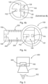
- Figure 1 shows a waveguide coupling device 100 according to an embodiment.
- the waveguide coupling device 100 comprises a high-frequency substrate 200 with an input conductor 106 which is connected to a first end of the high-frequency substrate 200 is arranged. It can be provided that the input conductor is not raised above the substrate.
- One or more excitation waves can be fed into the high-frequency substrate 200 via the input conductor, for example from a radar module. This first end is located in the direction of propagation of the excitation wave, in the direction of travel of the excitation wave and/or the longitudinal direction of the high-frequency substrate 200 opposite a second end of the high-frequency substrate 200, at which a radiation region 108 of the high-frequency substrate 200 is arranged.
- the input conductor 106 and the radiation region 108 are in turn coupled by a substrate-integrated waveguide 110, through which the excitation wave can run from the input conductor 106 to the radiation region 108.
- the waveguide coupling device 100 further comprises a waveguide 102, which is arranged with an excitation end 132 at, on and/or above the radiation region 108 of the high-frequency substrate 200.
- the excitation wave can be coupled at least partially into an internal volume 120 of the waveguide 102 via the radiation region 108.
- At least one first excitation element 112 and one second excitation element 114 are arranged in the area of the excitation end 132 of the waveguide 102.
- Each excitation element 112, 114 has a length 116, 118 measured in the longitudinal direction 134 of the waveguide 102.
- the lengths 116, 118 of the excitation elements 112, 114 are each measured from a lower edge of the corresponding excitation element 112, 114 to its upper edge.
- the lower edges of the excitation elements 112, 114 are flush with the end face of the waveguide 102 at the excitation end 132.
- the excitation elements 112, 114 could also be arranged offset from one another in the longitudinal direction 134.
- the excitation wave can generate at least two resonance waves of different resonance frequencies based on the excitation elements 112, 114.
- a first resonance wave can be formed on one of the excitation elements 112, 114 and a second resonance wave can be formed between the two excitation elements 112, 114, for example between their upper edges.
- one of the resonance waves can be formed on one of the excitation elements 112, 114 and a further structure of the waveguide 102 and/or a further excitation element.
- the lengths 116, 118 of the two excitation elements 112, 114 can be coordinated with one another in such a way that the resonance waves overlap, for example at least partially in phase and/or with a substantially identical phase position.
- the broadband of the signal can be, for example, in a range of 1-50 GHz, in particular around 10 GHz at a frequency of 80 GHz. With this type of coupling, bandwidths of over 10%, for example 12-15%, around 12-13%, can be achieved.
- phase-correct superposition can occur with signals of the same frequency. At different frequencies, the phases inevitably diverge somewhat. However, signals with different frequencies can be superimposed on one another and form a certain broadband through the frequency offset from one frequency to the other, for example as in Fig.6 can be seen.
- By superimposing two exciters or signals with the same frequency in the correct phase they can be amplified. This increases the efficiency of the entire device. This effect can be used, for example, between the two exciters 112 and 122.
- the spatial distance and the propagation time of the signal can also be used to set, influence and/or adjust the phase accordingly.
- the two excitation elements 112, 114 of the embodiment of the Figure 1 are rectangular and/or fin-like.
- the waveguide 102 is also designed as a circular waveguide 102, but can also be designed as a rectangular waveguide, for example.
- the excitation elements 112, 114 are spaced apart from one another in the radial direction of the waveguide 102.
- the two excitation elements 112, 114 protrude from the wall and/or inner surface of the waveguide 102 on opposite sides.
- the excitation elements 112, 114 of the waveguide 102 can also be viewed as fins or double fins.
- the first excitation element 112 can also be referred to as an exciter or resonator, whereby the second excitation element 114 can be referred to as a sub-exciter or sub-resonator, or vice versa.
- a geometry, size, shape, position, relative arrangement and/or relative alignment of the excitation elements 112, 114 can also be adapted and/or coordinated with one another to influence the resonance waves and/or resonance frequencies.
- One or more additional excitation elements can also be provided.
- FIG. 2 shows a high-frequency substrate 200 in plan view according to an embodiment.
- the high-frequency substrate 200 has an input conductor 106 for feeding in an incoming excitation wave.
- the high-frequency substrate 200 has a rectangular cross-section and has a substrate-integrated waveguide 110.
- the substrate-integrated waveguide 110 is formed between an upper copper layer 204a and a lower copper layer (not shown). Dielectric can be formed between the copper layers 204a, 204b.
- the substrate-integrated waveguide 110 thus resembles a filled waveguide.
- the two layers are connected with vias 202.
- the upper copper layer 204a has a breakthrough in the area of the radiation area 108 so that the excitation wave can emerge into the waveguide 102.
- the radiation area 108 is also delimited or surrounded by vias 202.
- the waveguide 102 can be mounted on the round portion 150 of the high frequency substrate 200 of the embodiment of the Figure 2 positioned, wherein the end face of the waveguide 102 faces the upper copper layer 204a and/or is arranged thereon, so that the radiation region 108 is encircled and/or enclosed by the waveguide 102 along its outer circumference.
- the substrate-integrated waveguide 110 has vias 202 which form a wall.
- the vias 202 can alternatively or additionally delimit the radiation region 108.
- the vias 202 connect the upper copper layer 204a and the lower copper layer 204b (in Fig. 2 not shown, see Fig. 3 ) electrically conductive to each other.
- FIG 3 shows a perspective view of the high frequency substrate 200 according to an embodiment.
- the high frequency substrate 200 of the Figure 3 the same elements and/or components as the high frequency substrate 200 of the Figure 2 on.
- the three layers of the high frequency substrate 200 are clearly visible.
- the upper copper layer 204a lies on a substrate layer 140, which in turn is arranged on the lower copper layer 204b.
- the two copper layers 204a, 204b or copper layers are connected to one another by means of the vias 202.
- the breakthrough in the upper copper layer 204a in the radiation area 108 is in the example of the embodiment of the Figure 3 clearly visible.
- FIG. 4a shows a waveguide coupling device 100 according to a further embodiment.
- the waveguide coupling device 100 of the Figure 4a the same elements and/or components as the waveguide coupling device 100 of the previous figures.
- the waveguide 102 of the embodiment of the Figure 4a is a round waveguide 102.
- the waveguide 102 of the embodiment of the Figure 4a further comprises a third excitation element 122.
- This third excitation element 122 is designed as a wall projection and protrudes from the wall or inner surface of the waveguide 102 into the inner volume 120.
- the third excitation element 122 can also be regarded as part of the wall of the waveguide 102.
- the second excitation element 114 protrudes from the third excitation element 122 into the inner volume 120.
- the length 124 of the third excitation element 122 measured in the longitudinal direction 134 is greater than that of the first excitation element 116, which in turn is greater than that of the second excitation element 118.
- the height 124 of the third excitation element 122 is adjusted in such a way that a third resonance wave is excited with a slight time delay to the first and second resonance waves.
- the third resonance wave can be excited between the first excitation element 112 and the third excitation element 122 (or between their upper edges), which has a third resonance frequency that is different from the first and second resonance frequencies.
- the radar signal 302 is formed by superimposing the three resonance waves, which then propagates towards the output of the waveguide 102 and can be emitted via an end opposite the excitation end 132.
- Figure 4b shows a section of the waveguide coupling device 100 according to the invention of the embodiment of Figure 4a along the line Ader Fig4a .
- the perspective of the cross-section of the Figure 4b is along the radiation direction of the radar signal and/or longitudinal extension direction 134 of the waveguide 102.
- the waveguide 102 of the Figure 4b further comprises two cavities 126, which are located on both sides of the second excitation element 114.
- the cavities 126 can serve to improve the manufacturability of the waveguide 102.
- the waveguide 102 of the Figure 4a and 4b is, as the Figure 4b can be seen, is formed integrally with the three excitation elements 114, 116, 122.
- Figure 4c shows a top view of the waveguide coupling device 100 according to an embodiment.
- Figure 4c it can be seen how the radiation region 108 is ring-shaped and enclosed by the waveguide 102, so that the excitation wave can penetrate into the inner volume of the waveguide 102.
- FIG. 5 shows a level measuring device 400 and/or a radar sensor 400 according to an embodiment.
- the level measuring device 400 of the embodiment of the Figure 5 has a radar module 300 and a waveguide coupling device 100.
- An excitation wave can be fed into the waveguide coupling device 100 via the radar module 300 and radiated, for example, via an antenna 301.
- Figure 6 shows a curve measured in a waveguide coupling device 100 according to an embodiment.
- the curve in Figure 6 The curve shown is a return loss curve, which is shown as a function of frequency.
- the curve is shown in the Figure 6 shown using a diagram.
- the vertical axis of the diagram shows the amplitude of the return loss curve in any unit.
- the amplitude can be specified in dB, for example.
- the horizontal axis shows a frequency in any unit.
- the frequency can be specified in GHz or MHz, for example.
- the measured curve of the Figure 6 may have been created by superposition and/or addition of three resonance waves. In the diagram of the Figure 6 Three resonance frequencies f1, f2, f3 are recognizable.
- the first resonance wave which can be formed at one of the excitation elements 112, 114 can have the resonance frequency f1.
- the second resonance wave which can be formed between the two excitation elements 112, 114, for example between their upper edges, can have the resonance frequency f2.
- the third resonance wave which can be excited between the first excitation element 112 and the third excitation element 122 (or between their upper edges) (see Figure 4a ), can have the resonance frequency f3.
- the three resonance frequencies f1, f2, f3 differ from each other.
- the diagram also shows the Figure 6 a possible bandwidth of the measured curve achieved by the design of the waveguide coupling device, in particular the excitation elements 112, 114, 122.
- the bandwidth of the radar signal 302 achieved by the design of the waveguide coupling device, in particular the excitation elements 112, 114, 122 can be directly or indirectly related to the bandwidth of the measured curve.
- This can, for example, refer to a frequency range of the measured curve in which the measured curve is below a given amplitude value B without interruption.
- the value B can, for example, be -10dB. However, other values for B are conceivable.
- This frequency range is between the frequencies f- and f+.
- Figure 7 shows a flowchart to illustrate a method according to an embodiment.
- step S1 at least one excitation wave is fed into a high-frequency substrate 200 of a waveguide coupling device 100.
- step S2 the excitation wave is coupled into an excitation end 132 of a waveguide 102 of the waveguide coupling device 100 via a radiation region 108 of the high-frequency substrate 200 of the waveguide coupling device 100, and in step S3, at least one first resonance wave with a first resonance frequency and one second resonance wave with a second resonance frequency are excited via the excitation wave on at least one first excitation element and one second excitation element 112, 114 of the waveguide 102.
- step S4 the radar signal 302 is emitted with the waveguide 102 of the waveguide coupling device 100 based on a superposition of at least the first resonance wave and the second resonance wave.
Landscapes
- Engineering & Computer Science (AREA)
- Radar, Positioning & Navigation (AREA)
- Remote Sensing (AREA)
- Computer Networks & Wireless Communication (AREA)
- Physics & Mathematics (AREA)
- General Physics & Mathematics (AREA)
- Control Of Motors That Do Not Use Commutators (AREA)
- Radar Systems Or Details Thereof (AREA)
- Waveguide Aerials (AREA)
Claims (14)
- Dispositif de couplage de guide d'ondes (100) pour un capteur radar (300), comportant :un guide d'ondes (102) pour émettre et/ou recevoir un signal radar (302) ; etun substrat à haute fréquence (200) qui comporte, à une première extrémité, au moins un conducteur d'entrée (106) pour injecter au moins une onde d'excitation dans le substrat à haute fréquence (200), à une seconde extrémité opposée à la première extrémité, une zone d'émission (108) avec un passage pour découpler l'onde d'excitation du substrat à haute fréquence (200), et un guide d'ondes (110) intégré au substrat, couplé au conducteur d'entrée (106) et à la zone d'émission (108) ;dans lequel une extrémité d'excitation (132) du guide d'ondes (102) est agencée sur la zone d'émission (108) du substrat à haute fréquence (200) de telle sorte que l'onde d'excitation peut être couplée dans l'extrémité d'excitation (132) du guide d'ondes (102) par l'intermédiaire de la zone d'émission (108) du substrat à haute fréquence (200) ;dans lequel le guide d'ondes (102) comporte au moins un premier élément d'excitation (112) et un deuxième élément d'excitation (114) qui sont respectivement agencés au niveau de l'extrémité d'excitation (132) dans un volume intérieur (120) du guide d'ondes (102) et qui s'étendent parallèlement à la direction d'extension longitudinale (134) du guide d'ondes (102) ;caractérisé en ce quele premier élément d'excitation (112) a une première longueur (116) mesurée dans la direction d'extension longitudinale (134) du guide d'ondes (102) et le deuxième élément d'excitation (114) a une deuxième longueur (118) mesurée dans la direction d'extension longitudinale (134) du guide d'ondes (102) qui est différente de la première longueur du premier élément d'excitation (116), de sorte qu'au moins une première onde de résonance ayant une première fréquence de résonance et une deuxième onde de résonance ayant une deuxième fréquence de résonance peuvent être excitées par l'intermédiaire de l'onde d'excitation au niveau du premier élément d'excitation (112) et du deuxième élément d'excitation (114), lesquelles ondes peuvent être superposées dans le guide d'ondes (102) en formant le signal radar (302), etdans lequel la zone d'émission (108) est limitée par des trous d'interconnexion et/ou le guide d'ondes (102) comporte deux cavités (126) qui sont situées des deux côtés du deuxième élément d'excitation (114).
- Dispositif de couplage de guide d'ondes (100) pour un capteur radar (300) selon la revendication 1,
dans lequel le premier élément d'excitation (112) et le deuxième élément d'excitation (114) font respectivement saillie au moins partiellement à partir d'une paroi du guide d'ondes (102) dans le volume intérieur (120) du guide d'ondes (102). - Dispositif de couplage de guide d'ondes (100) pour un capteur radar (300) selon l'une des revendications précédentes,
dans lequel le premier élément d'excitation (112) et le deuxième élément d'excitation (114) font saillie à partir de la paroi du guide d'ondes (102) sur deux côtés mutuellement opposés du guide d'ondes (102). - Dispositif de couplage de guide d'ondes (100) pour un capteur radar (300) selon l'une des revendications précédentes,
dans lequel au moins la première longueur (116) du premier élément d'excitation (112) et la deuxième longueur (118) du deuxième élément d'excitation (114) sont adaptées l'une à l'autre de telle sorte que la deuxième onde de résonance peut être générée de manière retardée par rapport à la première onde de résonance, que la première onde de résonance et la deuxième onde de résonance peuvent être superposées et peuvent en particulier être superposées de manière au moins partiellement en phase. - Dispositif de couplage de guide d'ondes (100) pour un capteur radar (300) selon l'une des revendications précédentes,
dans lequel le deuxième élément d'excitation est conçu pour générer la première onde de résonance et pour générer la deuxième onde de résonance entre les premier (112) et second (114) éléments d'excitation. - Dispositif de couplage de guide d'ondes (100) pour un capteur radar (300) selon l'une des revendications précédentes, comportant en outre :un troisième élément d'excitation (122) qui est agencé au niveau de l'extrémité d'excitation (132) dans le volume intérieur (120) du guide d'ondes (102) ;dans lequel le troisième élément d'excitation (122) a une troisième longueur (124) mesurée dans la direction d'extension longitudinale (134) du guide d'ondes (102), qui est différente de la première longueur (116) du premier élément d'excitation (112) et de la deuxième longueur (118) du deuxième élément d'excitation (114),dans lequel la troisième longueur (124) est dimensionnée et le troisième élément d'excitation est conçu de telle sorte qu'une troisième onde de résonance ayant une troisième fréquence de résonance peut être excitée par l'intermédiaire de l'onde d'excitation entre le premier élément d'excitation (112) et le troisième élément d'excitation (122).
- Dispositif de couplage de guide d'ondes (100) pour un capteur radar (300) selon la revendication 6,
dans lequel la première onde de résonance, la deuxième onde de résonance et la troisième onde de résonance peuvent être superposées au signal radar (302). - Dispositif de couplage de guide d'ondes (100) pour un capteur radar (300) selon la revendication 7,
dans lequel le deuxième élément d'excitation (114) fait saillie dans le volume intérieur (120) du guide d'ondes (102), à partir de la saillie de paroi formée par le troisième élément d'excitation (122). - Dispositif de couplage de guide d'ondes (100) pour un capteur radar (300) selon l'une des revendications 6 à 8,
dans lequel la première longueur (116) est plus grande que la deuxième longueur (118) et la troisième longueur (124) est plus grande que la première longueur (116). - Dispositif de couplage de guide d'ondes (100) pour un capteur radar (300) selon l'une des revendications précédentes,
dans lequel le substrat à haute fréquence (200) a une section transversale rectangulaire au moins dans une zone partielle. - Dispositif de couplage de guide d'ondes (100) pour un capteur radar (300) selon l'une des revendications précédentes,
dans lequel le guide d'ondes (102) du dispositif de couplage de guide d'ondes (100) est un guide d'ondes circulaire (102) . - Capteur radar (300) et/ou appareil de mesure de niveau de remplissage (400) comportant un dispositif de couplage de guide d'ondes (100) selon l'une des revendications précédentes.
- Utilisation d'un dispositif de couplage de guide d'ondes (100) selon l'une des revendications 1 à 11 dans un capteur radar (300) et/ou un appareil de mesure de niveau de remplissage (400) .
- Procédé pour générer et/ou recevoir un signal radar (302) avec un dispositif de couplage de guide d'ondes (100) selon l'une des revendications 1 à 11, comportant les étapes consistant à :injecter (S1) au moins une onde d'excitation dans un substrat à haute fréquence (200) d'un dispositif de couplage de guide d'ondes (100) ;coupler (S2) l'onde d'excitation dans une extrémité d'excitation (132) d'un guide d'ondes (102) du dispositif de couplage de guide d'ondes (100), par l'intermédiaire d'une zone d'émission (108) du substrat à haute fréquence (200) du dispositif de couplage de guide d'ondes (100) ;exciter (S3), par l'intermédiaire de l'onde d'excitation au niveau d'au moins un premier élément d'excitation et un deuxième élément d'excitation (112, 114) du guide d'ondes (102), au moins une première onde de résonance ayant une première fréquence de résonance et une deuxième onde de résonance ayant une deuxième fréquence de résonance ; etémettre (S4) le signal radar (302) avec le guide d'ondes (102) du dispositif de couplage de guide d'ondes (100) sur la base d'une superposition d'au moins la première onde de résonance et la deuxième onde de résonance ; et/ou recevoir un signal radar réfléchi avec le guide d'ondes (102) du dispositif de couplage de guide d'ondes (100).
Priority Applications (3)
| Application Number | Priority Date | Filing Date | Title |
|---|---|---|---|
| EP20190652.6A EP3955376B1 (fr) | 2020-08-12 | 2020-08-12 | Dispositif d'accouplement d'un guide d'ondes pour un capteur radar |
| CN202110909187.7A CN114079134B (zh) | 2020-08-12 | 2021-08-09 | 用于雷达传感器的波导耦合装置 |
| US17/398,676 US12117557B2 (en) | 2020-08-12 | 2021-08-10 | Waveguide coupling device for a radar sensor |
Applications Claiming Priority (1)
| Application Number | Priority Date | Filing Date | Title |
|---|---|---|---|
| EP20190652.6A EP3955376B1 (fr) | 2020-08-12 | 2020-08-12 | Dispositif d'accouplement d'un guide d'ondes pour un capteur radar |
Publications (3)
| Publication Number | Publication Date |
|---|---|
| EP3955376A1 EP3955376A1 (fr) | 2022-02-16 |
| EP3955376C0 EP3955376C0 (fr) | 2025-01-01 |
| EP3955376B1 true EP3955376B1 (fr) | 2025-01-01 |
Family
ID=72050702
Family Applications (1)
| Application Number | Title | Priority Date | Filing Date |
|---|---|---|---|
| EP20190652.6A Active EP3955376B1 (fr) | 2020-08-12 | 2020-08-12 | Dispositif d'accouplement d'un guide d'ondes pour un capteur radar |
Country Status (3)
| Country | Link |
|---|---|
| US (1) | US12117557B2 (fr) |
| EP (1) | EP3955376B1 (fr) |
| CN (1) | CN114079134B (fr) |
Families Citing this family (3)
| Publication number | Priority date | Publication date | Assignee | Title |
|---|---|---|---|---|
| CN114221122B (zh) * | 2022-02-21 | 2022-05-17 | 成都华兴大地科技有限公司 | 双端口同极化天线 |
| DE102022202220A1 (de) * | 2022-03-04 | 2023-09-07 | Robert Bosch Gesellschaft mit beschränkter Haftung | Vorrichtung für einen Übergang einer Hochfrequenzverbindung zwischen einer Streifenleiterverbindung und einem Hohlleiter, Hochfrequenzanordnung und Radarsystem |
| CN119208956B (zh) * | 2024-11-12 | 2026-04-03 | 南通大学 | 一种具备滤波及高定向性的基片集成波导耦合器 |
Family Cites Families (17)
| Publication number | Priority date | Publication date | Assignee | Title |
|---|---|---|---|---|
| JPS518709B1 (fr) | 1970-12-23 | 1976-03-19 | ||
| GB8929300D0 (en) * | 1989-12-29 | 1990-02-28 | Instrumentarium Corp | Apparatus |
| EP1333526A1 (fr) * | 2002-01-30 | 2003-08-06 | Alcatel | Transition entre une ligne microruban et un guide d'ondes |
| DE102006032346A1 (de) * | 2006-07-12 | 2008-01-17 | Siemens Ag | Vorrichtung zur Messung von Füllständen in einem Kraftstoffbehälter |
| JP4622954B2 (ja) * | 2006-08-01 | 2011-02-02 | 株式会社デンソー | 線路導波管変換器および無線通信装置 |
| DE102006055409A1 (de) * | 2006-11-22 | 2008-05-29 | Ab Elektronik Gmbh | Induktiver Sensor zur Erfassung von zwei Koppelelementen |
| EP2652462B1 (fr) * | 2010-12-16 | 2016-08-24 | VEGA Grieshaber KG | Dispositif de mesure, dispositif de commande et appareil de mesure pour la mesure d'un niveau |
| DE102013108434B4 (de) | 2013-08-05 | 2020-06-25 | Finetek Co., Ltd. | Hornantennenvorrichtung und stufenförmige Signaleinspeisevorrichtung hierfür |
| JP6417329B2 (ja) * | 2013-10-01 | 2018-11-07 | ソニーセミコンダクタソリューションズ株式会社 | コネクタ装置及び通信システム |
| FR3024802B1 (fr) * | 2014-08-11 | 2016-09-09 | Zodiac Data Systems | Source multibande a cornet coaxial avec systemes de poursuite monopulse pour antenne a reflecteur |
| DE102015218877B4 (de) * | 2015-09-30 | 2017-08-31 | Airbus Ds Gmbh | Koaxialer Diplexer und Signalkopplungseinrichtung |
| US10283832B1 (en) * | 2017-12-26 | 2019-05-07 | Vayyar Imaging Ltd. | Cavity backed slot antenna with in-cavity resonators |
| DE102018118765A1 (de) * | 2018-08-02 | 2020-02-06 | Endress+Hauser SE+Co. KG | Hochfrequenzbaustein |
| DE102020200882A1 (de) | 2019-01-30 | 2020-07-30 | i-Pego GmbH | Inserter, Adapter und Anzeigeeinrichtung zur Einführung eines Platzhalters in der Wirbelsäulenchirurgie |
| DE102019204671A1 (de) | 2019-04-02 | 2020-10-08 | Vega Grieshaber Kg | Radarmodul mit Doppelfinne |
| CN110739513B (zh) * | 2019-10-12 | 2021-08-31 | 南京理工大学 | 一种Ka频段波导同轴转换器 |
| EP3839453B1 (fr) * | 2019-12-20 | 2023-06-14 | Universität Potsdam | Agencement de mesure pour spectromètre optique |
-
2020
- 2020-08-12 EP EP20190652.6A patent/EP3955376B1/fr active Active
-
2021
- 2021-08-09 CN CN202110909187.7A patent/CN114079134B/zh active Active
- 2021-08-10 US US17/398,676 patent/US12117557B2/en active Active
Also Published As
| Publication number | Publication date |
|---|---|
| EP3955376C0 (fr) | 2025-01-01 |
| US12117557B2 (en) | 2024-10-15 |
| EP3955376A1 (fr) | 2022-02-16 |
| CN114079134B (zh) | 2026-01-27 |
| CN114079134A (zh) | 2022-02-22 |
| US20220050170A1 (en) | 2022-02-17 |
Similar Documents
| Publication | Publication Date | Title |
|---|---|---|
| DE102014203185B4 (de) | Antennenvorrichtung und Radarvorrichtung | |
| DE69821327T2 (de) | Kurzgeschlossene Streifenleiterantenne und Gerät damit | |
| EP1547192B1 (fr) | Dispositif pour transmettre ou emettre des ondes haute frequence | |
| DE69615101T2 (de) | Nichtstrahlendes dielektrisches Wellenleitergerät und Instrument zur Messung der Charakteristika einer Leiterplatte | |
| EP3955376B1 (fr) | Dispositif d'accouplement d'un guide d'ondes pour un capteur radar | |
| DE69938413T2 (de) | Planare antenne und verfahren zur herstellung derselben | |
| DE19813767C2 (de) | Mikrowellen-Sender /Empfängermodul | |
| DE69826223T2 (de) | In Mikrostreifenleitungstechnik ausgeführte Antenne und diese enthaltende Vorrichtung | |
| DE112004000077B4 (de) | Verdrillter Wellenleiter und drahtlose Vorrichtung | |
| DE112018004977B4 (de) | Hochfrequenzübertragungsleitung | |
| DE69823591T2 (de) | Geschichtete Aperturantenne und mehrschichtige Leiterplatte damit | |
| DE69731030T2 (de) | Funksendeempfänger | |
| DE10120248A1 (de) | Struktur zur Verbindung eines nicht strahlenden dielektrischen Wellenleiters und eines Metallwellenleiters, Sende-/Empfangsmodul für Millimeterwellen und Sender/Empfänger für Millimeterwellen | |
| DE2942035C2 (de) | Einrichtung zum Empfang von Mikrowellen | |
| DE102007056258A1 (de) | Chipantenne sowie mobiles Telekommunikationsendgerät, welches diese aufweist | |
| DE112008001621T5 (de) | Gleichstromsperrschaltung, Hybridschaltungsvorrichtung, Sender, Empfänger, Sender-Empfänger und Radarvorrichtung | |
| DE10351506A1 (de) | Vorrichtung sowie Verfahren zur Phasenverschiebung | |
| DE102010020022A1 (de) | Fahrerassistenzeinrichtung für ein Fahrzeug, Fahrzeug und Verfahren zum Betreiben eines Radargeräts | |
| DE10353686A1 (de) | Symmetrische Antenne in Schichtbauweise | |
| DE10050544A1 (de) | Ein nicht strahlender Dielektrischer Wellenleiter und eine Millimeterwellen-Sende-/Empfangsvorrichtung | |
| WO2013120994A1 (fr) | Agencement de circuit imprimé pour alimenter des antennes par un système à trois fils afin d'exciter des polarisations différentes | |
| EP4062487A1 (fr) | Puce radar à couplage de guide d'ondes | |
| DE60224012T2 (de) | Mikrostreifenleitungsübergang | |
| DE69626332T2 (de) | Dielektrische Planarleitung und integrierte Schaltung die dieselbe benutzt | |
| MXPA05007249A (es) | Transicion entre una guia de ondas rectangular y una linea de microtiras. |
Legal Events
| Date | Code | Title | Description |
|---|---|---|---|
| PUAI | Public reference made under article 153(3) epc to a published international application that has entered the european phase |
Free format text: ORIGINAL CODE: 0009012 |
|
| STAA | Information on the status of an ep patent application or granted ep patent |
Free format text: STATUS: THE APPLICATION HAS BEEN PUBLISHED |
|
| AK | Designated contracting states |
Kind code of ref document: A1 Designated state(s): AL AT BE BG CH CY CZ DE DK EE ES FI FR GB GR HR HU IE IS IT LI LT LU LV MC MK MT NL NO PL PT RO RS SE SI SK SM TR |
|
| STAA | Information on the status of an ep patent application or granted ep patent |
Free format text: STATUS: REQUEST FOR EXAMINATION WAS MADE |
|
| 17P | Request for examination filed |
Effective date: 20220810 |
|
| RBV | Designated contracting states (corrected) |
Designated state(s): AL AT BE BG CH CY CZ DE DK EE ES FI FR GB GR HR HU IE IS IT LI LT LU LV MC MK MT NL NO PL PT RO RS SE SI SK SM TR |
|
| STAA | Information on the status of an ep patent application or granted ep patent |
Free format text: STATUS: EXAMINATION IS IN PROGRESS |
|
| 17Q | First examination report despatched |
Effective date: 20230327 |
|
| REG | Reference to a national code |
Ref country code: DE Ref legal event code: R079 Free format text: PREVIOUS MAIN CLASS: H01P0005107000 Ipc: H01P0005080000 Ref country code: DE Ref legal event code: R079 Ref document number: 502020010083 Country of ref document: DE Free format text: PREVIOUS MAIN CLASS: H01P0005107000 Ipc: H01P0005080000 |
|
| GRAP | Despatch of communication of intention to grant a patent |
Free format text: ORIGINAL CODE: EPIDOSNIGR1 |
|
| RIC1 | Information provided on ipc code assigned before grant |
Ipc: H01Q 13/06 20060101ALN20240717BHEP Ipc: H01Q 5/55 20150101ALI20240717BHEP Ipc: H01Q 1/22 20060101ALI20240717BHEP Ipc: H01P 5/08 20060101AFI20240717BHEP |
|
| STAA | Information on the status of an ep patent application or granted ep patent |
Free format text: STATUS: GRANT OF PATENT IS INTENDED |
|
| INTG | Intention to grant announced |
Effective date: 20240822 |
|
| GRAS | Grant fee paid |
Free format text: ORIGINAL CODE: EPIDOSNIGR3 |
|
| GRAA | (expected) grant |
Free format text: ORIGINAL CODE: 0009210 |
|
| STAA | Information on the status of an ep patent application or granted ep patent |
Free format text: STATUS: THE PATENT HAS BEEN GRANTED |
|
| AK | Designated contracting states |
Kind code of ref document: B1 Designated state(s): AL AT BE BG CH CY CZ DE DK EE ES FI FR GB GR HR HU IE IS IT LI LT LU LV MC MK MT NL NO PL PT RO RS SE SI SK SM TR |
|
| RAP3 | Party data changed (applicant data changed or rights of an application transferred) |
Owner name: VEGA GRIESHABER KG |
|
| REG | Reference to a national code |
Ref country code: GB Ref legal event code: FG4D Free format text: NOT ENGLISH |
|
| REG | Reference to a national code |
Ref country code: CH Ref legal event code: EP |
|
| REG | Reference to a national code |
Ref country code: DE Ref legal event code: R096 Ref document number: 502020010083 Country of ref document: DE |
|
| REG | Reference to a national code |
Ref country code: IE Ref legal event code: FG4D Free format text: LANGUAGE OF EP DOCUMENT: GERMAN |
|
| U01 | Request for unitary effect filed |
Effective date: 20250131 |
|
| U07 | Unitary effect registered |
Designated state(s): AT BE BG DE DK EE FI FR IT LT LU LV MT NL PT RO SE SI Effective date: 20250206 |
|
| PG25 | Lapsed in a contracting state [announced via postgrant information from national office to epo] |
Ref country code: PL Free format text: LAPSE BECAUSE OF FAILURE TO SUBMIT A TRANSLATION OF THE DESCRIPTION OR TO PAY THE FEE WITHIN THE PRESCRIBED TIME-LIMIT Effective date: 20250101 |
|
| PG25 | Lapsed in a contracting state [announced via postgrant information from national office to epo] |
Ref country code: ES Free format text: LAPSE BECAUSE OF FAILURE TO SUBMIT A TRANSLATION OF THE DESCRIPTION OR TO PAY THE FEE WITHIN THE PRESCRIBED TIME-LIMIT Effective date: 20250101 |
|
| PG25 | Lapsed in a contracting state [announced via postgrant information from national office to epo] |
Ref country code: NO Free format text: LAPSE BECAUSE OF FAILURE TO SUBMIT A TRANSLATION OF THE DESCRIPTION OR TO PAY THE FEE WITHIN THE PRESCRIBED TIME-LIMIT Effective date: 20250401 Ref country code: IS Free format text: LAPSE BECAUSE OF FAILURE TO SUBMIT A TRANSLATION OF THE DESCRIPTION OR TO PAY THE FEE WITHIN THE PRESCRIBED TIME-LIMIT Effective date: 20250501 |
|
| PG25 | Lapsed in a contracting state [announced via postgrant information from national office to epo] |
Ref country code: HR Free format text: LAPSE BECAUSE OF FAILURE TO SUBMIT A TRANSLATION OF THE DESCRIPTION OR TO PAY THE FEE WITHIN THE PRESCRIBED TIME-LIMIT Effective date: 20250101 |
|
| PG25 | Lapsed in a contracting state [announced via postgrant information from national office to epo] |
Ref country code: GR Free format text: LAPSE BECAUSE OF FAILURE TO SUBMIT A TRANSLATION OF THE DESCRIPTION OR TO PAY THE FEE WITHIN THE PRESCRIBED TIME-LIMIT Effective date: 20250402 |
|
| PG25 | Lapsed in a contracting state [announced via postgrant information from national office to epo] |
Ref country code: CZ Free format text: LAPSE BECAUSE OF FAILURE TO SUBMIT A TRANSLATION OF THE DESCRIPTION OR TO PAY THE FEE WITHIN THE PRESCRIBED TIME-LIMIT Effective date: 20250101 |
|
| U20 | Renewal fee for the european patent with unitary effect paid |
Year of fee payment: 6 Effective date: 20250826 |
|
| PG25 | Lapsed in a contracting state [announced via postgrant information from national office to epo] |
Ref country code: SM Free format text: LAPSE BECAUSE OF FAILURE TO SUBMIT A TRANSLATION OF THE DESCRIPTION OR TO PAY THE FEE WITHIN THE PRESCRIBED TIME-LIMIT Effective date: 20250101 |
|
| PGFP | Annual fee paid to national office [announced via postgrant information from national office to epo] |
Ref country code: GB Payment date: 20250822 Year of fee payment: 6 |
|
| PG25 | Lapsed in a contracting state [announced via postgrant information from national office to epo] |
Ref country code: SK Free format text: LAPSE BECAUSE OF FAILURE TO SUBMIT A TRANSLATION OF THE DESCRIPTION OR TO PAY THE FEE WITHIN THE PRESCRIBED TIME-LIMIT Effective date: 20250101 |
|
| PLBE | No opposition filed within time limit |
Free format text: ORIGINAL CODE: 0009261 |
|
| STAA | Information on the status of an ep patent application or granted ep patent |
Free format text: STATUS: NO OPPOSITION FILED WITHIN TIME LIMIT |
|
| REG | Reference to a national code |
Ref country code: CH Ref legal event code: L10 Free format text: ST27 STATUS EVENT CODE: U-0-0-L10-L00 (AS PROVIDED BY THE NATIONAL OFFICE) Effective date: 20251112 |
|
| 26N | No opposition filed |
Effective date: 20251002 |
|
| REG | Reference to a national code |
Ref country code: CH Ref legal event code: H13 Free format text: ST27 STATUS EVENT CODE: U-0-0-H10-H13 (AS PROVIDED BY THE NATIONAL OFFICE) Effective date: 20260324 |
|
| PG25 | Lapsed in a contracting state [announced via postgrant information from national office to epo] |
Ref country code: MC Free format text: LAPSE BECAUSE OF FAILURE TO SUBMIT A TRANSLATION OF THE DESCRIPTION OR TO PAY THE FEE WITHIN THE PRESCRIBED TIME-LIMIT Effective date: 20250101 |