EP4035263B1 - Oscillateurs à stabilité améliorée utilisant un peigne phononique - Google Patents
Oscillateurs à stabilité améliorée utilisant un peigne phononique Download PDFInfo
- Publication number
- EP4035263B1 EP4035263B1 EP20867516.5A EP20867516A EP4035263B1 EP 4035263 B1 EP4035263 B1 EP 4035263B1 EP 20867516 A EP20867516 A EP 20867516A EP 4035263 B1 EP4035263 B1 EP 4035263B1
- Authority
- EP
- European Patent Office
- Prior art keywords
- frequency
- comb
- oscillator
- voltage controlled
- controlled oscillator
- Prior art date
- Legal status (The legal status is an assumption and is not a legal conclusion. Google has not performed a legal analysis and makes no representation as to the accuracy of the status listed.)
- Active
Links
Images

Classifications
-
- G—PHYSICS
- G02—OPTICS
- G02F—OPTICAL DEVICES OR ARRANGEMENTS FOR THE CONTROL OF LIGHT BY MODIFICATION OF THE OPTICAL PROPERTIES OF THE MEDIA OF THE ELEMENTS INVOLVED THEREIN; NON-LINEAR OPTICS; FREQUENCY-CHANGING OF LIGHT; OPTICAL LOGIC ELEMENTS; OPTICAL ANALOGUE/DIGITAL CONVERTERS
- G02F1/00—Devices or arrangements for the control of the intensity, colour, phase, polarisation or direction of light arriving from an independent light source, e.g. switching, gating or modulating; Non-linear optics
- G02F1/35—Non-linear optics
- G02F1/353—Frequency conversion, i.e. wherein a light beam is generated with frequency components different from those of the incident light beams
-
- G—PHYSICS
- G04—HOROLOGY
- G04G—ELECTRONIC TIME-PIECES
- G04G3/00—Producing timing pulses
- G04G3/04—Temperature-compensating arrangements
-
- H—ELECTRICITY
- H03—ELECTRONIC CIRCUITRY
- H03B—GENERATION OF OSCILLATIONS, DIRECTLY OR BY FREQUENCY-CHANGING, BY CIRCUITS EMPLOYING ACTIVE ELEMENTS WHICH OPERATE IN A NON-SWITCHING MANNER; GENERATION OF NOISE BY SUCH CIRCUITS
- H03B5/00—Generation of oscillations using amplifier with regenerative feedback from output to input
- H03B5/02—Details
- H03B5/04—Modifications of generator to compensate for variations in physical values, e.g. power supply, load, temperature
-
- H—ELECTRICITY
- H03—ELECTRONIC CIRCUITRY
- H03B—GENERATION OF OSCILLATIONS, DIRECTLY OR BY FREQUENCY-CHANGING, BY CIRCUITS EMPLOYING ACTIVE ELEMENTS WHICH OPERATE IN A NON-SWITCHING MANNER; GENERATION OF NOISE BY SUCH CIRCUITS
- H03B5/00—Generation of oscillations using amplifier with regenerative feedback from output to input
- H03B5/30—Generation of oscillations using amplifier with regenerative feedback from output to input with frequency-determining element being electromechanical resonator
- H03B5/32—Generation of oscillations using amplifier with regenerative feedback from output to input with frequency-determining element being electromechanical resonator being a piezoelectric resonator
- H03B5/36—Generation of oscillations using amplifier with regenerative feedback from output to input with frequency-determining element being electromechanical resonator being a piezoelectric resonator active element in amplifier being semiconductor device
- H03B5/366—Generation of oscillations using amplifier with regenerative feedback from output to input with frequency-determining element being electromechanical resonator being a piezoelectric resonator active element in amplifier being semiconductor device and comprising means for varying the frequency by a variable voltage or current
-
- H—ELECTRICITY
- H03—ELECTRONIC CIRCUITRY
- H03L—AUTOMATIC CONTROL, STARTING, SYNCHRONISATION OR STABILISATION OF GENERATORS OF ELECTRONIC OSCILLATIONS OR PULSES
- H03L7/00—Automatic control of frequency or phase; Synchronisation
- H03L7/06—Automatic control of frequency or phase; Synchronisation using a reference signal applied to a frequency- or phase-locked loop
-
- G—PHYSICS
- G02—OPTICS
- G02F—OPTICAL DEVICES OR ARRANGEMENTS FOR THE CONTROL OF LIGHT BY MODIFICATION OF THE OPTICAL PROPERTIES OF THE MEDIA OF THE ELEMENTS INVOLVED THEREIN; NON-LINEAR OPTICS; FREQUENCY-CHANGING OF LIGHT; OPTICAL LOGIC ELEMENTS; OPTICAL ANALOGUE/DIGITAL CONVERTERS
- G02F2203/00—Function characteristic
- G02F2203/54—Optical pulse train (comb) synthesizer
-
- G—PHYSICS
- G02—OPTICS
- G02F—OPTICAL DEVICES OR ARRANGEMENTS FOR THE CONTROL OF LIGHT BY MODIFICATION OF THE OPTICAL PROPERTIES OF THE MEDIA OF THE ELEMENTS INVOLVED THEREIN; NON-LINEAR OPTICS; FREQUENCY-CHANGING OF LIGHT; OPTICAL LOGIC ELEMENTS; OPTICAL ANALOGUE/DIGITAL CONVERTERS
- G02F2203/00—Function characteristic
- G02F2203/56—Frequency comb synthesizer
-
- H—ELECTRICITY
- H03—ELECTRONIC CIRCUITRY
- H03H—IMPEDANCE NETWORKS, e.g. RESONANT CIRCUITS; RESONATORS
- H03H9/00—Networks comprising electromechanical or electro-acoustic elements; Electromechanical resonators
- H03H9/15—Constructional features of resonators consisting of piezoelectric or electrostrictive material
- H03H9/17—Constructional features of resonators consisting of piezoelectric or electrostrictive material having a single resonator
- H03H9/19—Constructional features of resonators consisting of piezoelectric or electrostrictive material having a single resonator consisting of quartz
Definitions
- Quartz oscillators was used in many applications in today's electronics. Low phase noise is required for many applications of quartz oscillators including radar, navigation, and communication applications. There has a continuous need to improve the phase noise and reduce the Size, Weight and Power (SWaP) of reference oscillators. Nonlinear effects such as Duffing effects in MEMS resonators has been explored in the past to improve phase noise.
- SWaP Size, Weight and Power
- Temperature Compensated Crystal Oscillators are used in many clock applications and have a small size and low power (typically around 15 mm 3 and ⁇ 10 mW, respectively). However, they can drift about 0.2 ppm over temperature and have typical phase noise of -90 dBc/Hz @ 10 Hz. Low cost TCXOs have g-sensitivities of 1 x 10 -9 /g, and g-hardened TCXOs can have g-sensitivities of ⁇ 2 - 5 x 10 -11 /g. To achieve higher stability, Oven Controlled Crystal Oscillators (OCXOs) may be used.
- Oven Controlled Crystal Oscillators Oven Controlled Crystal Oscillators
- OCXOs typically have larger volumes of about 1000 mm 3 and use > 150 mW of power. They provide temperature stability of ⁇ 50 ppb and phase noise of around -120 dBc/Hz @ 10 Hz. However, OCXOs can have higher g-sensitivity than g-hardened TCXOs. To further improve the temperature stability and phase noise at lower offset frequencies, Chip-Scale Atomic Clocks (CSAC) have been developed. However, their size and power are even larger than OCXOs by roughly an order of magnitude and their g-sensitivity can be orders of magnitude worse than a TCXO. Thus, there is a need for a true chip-scale clock with TCXO-like power requirement, but higher stability than a TCXO, and g-sensitivities in the 10 -11 /g range.
- CRC Chip-Scale Atomic Clocks
- nonlinear Duffing effects have be used in the past for attempting to improve the phase noise of low cost MEMS oscillators, including those made from quartz, AIN, and silicon. See, for example, D. T. Chang, H. P. Moyer, R. G. Nagele, R. L. Kubena, R. J. Joyce, D. J. Kirby, P. D. Brewer, H. D. Nguyen, and F. P. Stratton, "Nonlinear UHF Quartz MEMS Oscillator with Phase Noise Reduction," 26th IEEE International Conference on MicroElectroMechanical Systems, Taipei, Taiwan, Jan. 20-24, 2013 .
- Phononic combs form when one or more high-Q resonances are driven slightly off their resonant frequency into a nonlinear state.
- the inventors of the present invention demonstrate that phononic combs can be created in high Q quartz resonators. Teeth in these combs exhibit complex behavior relative to the drive frequency and can be used to enhance or suppress frequency shifts in the system.
- KR 20120132987 discloses a phase locked oscillator using a comb generator, that is provided to output a harmonic component from which the phase noise of 10Ghz is removed by removing a second harmonic component of a desired signal using a lowpass filter.
- the phase locked oscillator comprises a digital PPL(phase locked loop)(21) and a comb generator unit(22).
- the digital PPL unit comprises a PLL unit(1), a first loop filter(2), a voltage controlled SAW(surface acoustic wave) Resonator(3), a low pass filter(4), a first amplifier(5), and an attenuator(6).
- a difference component which is compared with a phase through the PLL unit is outputted as an error signal through a charge pump.
- a first loop filter removes noises and high frequency components.
- a comb generator unit comprises a comb generator(7), a high pass filter(8), a band pass filter(9), an amplifier(10), a band pass filter(11), an amplifier(12), and a low pass filter(13).
- US 2014/021986 discloses a variable frequency synthesizer and method of outputting the variable frequency.
- the synthesizer comprises a first reference frequency, a direct digital synthesizer (DDS) receiving the first reference frequency and outputting a tuned frequency, a variable frequency comb generator receiving the tuned frequency and outputting a variable frequency comb comprised of a plurality of comb lines, a mixer receiving the variable frequency comb and a signal from an oscillator and outputting an intermediate frequency, a phase lock loop (PLL) receiving a second reference frequency and the intermediate frequency and outputting a phase lock signal, and the oscillator receiving the phase lock signal and outputting a variable synthesized frequency.
- DDS direct digital synthesizer
- PLL phase lock loop
- KR 2008 0044977 discloses a phase locked loop and a method for operating the same, that are provided to reduce an area thereof by sharing a charge pump in a receiving phase locked loop and a transmitting phase locked loop.
- a first voltage controlled oscillator(222) is connected to a first loop filter(221).
- a second voltage controlled oscillator(232) is connected to a second loop filter(231).
- a first switching circuit(211) outputs a feedback signal outputted from the first voltage controlled oscillator or a feedback signal outputted from the second voltage controlled oscillator in response to a switching control signal.
- a phase detector(212) receives a reference signal and an output signal of the first switching circuit and generates a control signal corresponding to a phase difference between the received signals.
- a charge pump(213) is connected to the phase detector.
- a second switching circuit(214) is formed to connect an output terminal of the charge pump with an input terminal of the first loop filter or an input terminal of the second loop filter in response to the switching control signal.
- US 2018/157148 discloses a photon generator that includes a frequency comb generator configured to generate a frequency comb of a predetermined frequency band, and a controller configured to perform frequency locking for frequency stabilization of an optical frequency generated by the frequency comb generator
- WO 2009/098686 discloses a solid state atomic clock that may utilize quantum states and is capable of exhibiting a hyperfine resonance in order to generate a frequency standard.
- a device capable of coupling a free running oscillator to the hyperfine resonance frequency in order to generated output signal is described herein.
- the atomic clock may be fabricated on a silicon substrate and it may be integrated, in chip scale, as part of an electronic integrated circuit. The principal of operation, the method of making and system which utilized a solid state atomic clock are also disclosed.
- the letter portrays the well-connected process of phononic frequency comb formation and defines the attributes to control the features associated with comb formation in such a system.
- the interplay between the nonlinear resonances and the well-known Duffing phenomenon is also observed.
- This disclosure describes a method of using a phononic frequency comb to enhance the stability of an oscillator.
- a phononic comb When a phononic comb is produced through modal mixing of local modes within the resonator which is driven slightly off one of its resonant frequencies, the comb teeth can exhibit regions of low drive frequency sensitivity. This effect can be utilized to provide a high stability reference for locking a second voltage-controlled crystal oscillator (VCXO).
- VCXO voltage-controlled crystal oscillator
- the output of a second VCXO can be stabilized compared to its own native stability. This can be done with only a modest increase in size and power compared to a single VCXO since MEMS-based VCXOs can be integrated in arrays on a single Si wafer with each resonator only requiring ⁇ 1 mm 2 of space.
- the drive and reference element can be ovenized to increase the stability over temperature or modes can be used which are temperature compensated.
- modes can be used which are temperature compensated.
- resonant mode sensors such as temperature, pressure, and acceleration sensors
- the more sensitive teeth in the comb can be used to enhance frequency shifts induced by input stimuli.
- stable comb teeth can be used to reduce noise.
- the presently disclosed technology provides an oscillator comprising: a first voltage controlled oscillator, a nonlinear resonator element, a second voltage controlled oscillator, and a Phase Locked Loop (PLL) circuit; wherein the first voltage controlled oscillator comprises at least a first resonator and its sustaining circuit, wherein the first oscillator drives the nonlinear resonator element producing a frequency comb, wherein the second voltage controlled oscillator is locked, in use, to a selected tooth of the comb at a frequency in which the first derivative of the drive frequency versus the frequency of the selected tooth in the comb has an absolute value greater than 1, and wherein the PLL circuit controls the locking of the second voltage controlled oscillator to the frequency of the selected tooth.
- PLL Phase Locked Loop
- an oscillator comprising: a plurality of piezoelectric resonators; first and second sustaining circuits coupled to first and second ones of the plurality of piezoelectric resonators, wherein the first of the sustaining circuits generates a drive signal of given frequency that is applied to another one of said plurality of piezoelectric resonators which generates a frequency comb signal; wherein the second of the sustaining circuits is coupled with a phase locked loop system, the second one of the resonators being locked to a selected tooth of the frequency comb signal at a particular frequency for which a first derivative of the drive frequency signal versus the frequency of the selected tooth has an absolute value greater than one; and wherein the PLL system controls the locking of the second oscillator to the selected tooth of the comb wherein said first derivative has an absolute value greater than one.
- the presently disclosed technology provides a method for enhancing the stability of an oscillator circuit by generating a comb of frequencies in a non-linear resonator member in response to a drive frequency, the oscillator circuit including a voltage controlled oscillator which is locked to a particular or selected tooth of the comb of frequencies produced by the non-linear resonator member at a drive frequency for which an absolute value of the first derivative of the drive frequency versus said frequency of a particular tooth of the comb is greater than 1, the voltage controlled oscillator being coupled with a PLL circuit for controlling the locking of the voltage controlled oscillator to said particular or selected tooth of the comb of frequencies.
- the presently disclosed technology provides an oscillator circuit, the oscillator circuit generating a drive signal, the oscillator circuit including a non-linear resonator member which generates, in use, a comb of frequencies in response to said drive signal, the oscillator circuit including a voltage controlled oscillator and a PLL, the voltage controlled oscillator being locked by the PLL to a particular or selected tooth of the comb of frequencies produced by the non-linear resonator member at a drive signal frequency for which an absolute value of the first derivative of the drive frequency versus said frequency of a particular tooth of the comb is greater than one.
- An apparatus and method for increasing the stability of a quartz oscillator by generating a phononic comb in a nonlinear quartz resonator and selecting a tooth in said comb for which a first derivative of the drive frequency versus the frequency of the selected tooth in a comb has an absolute value greater than one to thereby reduce frequency instability of the quartz oscillator.
- An apparatus and method for increasing the stability of quartz oscillators by using a phononic comb generated in a nonlinear resonator, preferably embodied by a quartz MEMS electro-mechanical resonator, to reduce the frequency instability.
- a frequency comb has been shown to exhibit regions in which the frequency of particular teeth are insensitive (or substantially insensitive) to changes in the difference between a drive frequency (from a crystal oscillator - the "drive oscillator” also preferably embodied by another quartz MEMS electro-mechanical resonator) and the resonator modal frequency of the nonlinear resonator.
- PLL phase-locked loop
- VCXO voltage-controlled crystal oscillator
- This effect can be utilized to provide a high stability reference for locking a second VCXO.
- the output of the second VCXO can be stabilized compared to its own native stability. This can be done with only a modest increase in size and power compared to a single VCXO since MEMS-based VCXOs can be integrated in arrays on a single Si wafer with each resonator only requiring ⁇ 1 mm 2 .
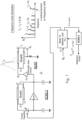
- FIG. 1 An embodiment of the disclosed technology is now described with reference to Fig. 1 with supporting data of a quartz AT-cut resonator frequency comb shown in Figs. 2 , 3 and 4 .
- Fig. 1 shows the basic components of embodiment of the present invention as a first VCXO (VCXO1) comprising two resonators 30 and 40, a second VCXO (VCXO2) acting as the sensor or oscillator and electronics comprising a mixer, a phase detector, and a PLL circuit.
- a drive signal generated by a first VCXO (VCXO1) is preferably amplified and stabilized with an automatic gain control circuit 38.
- the output Si at frequency f D is applied to resonator 40 having a resonant mode at a frequency fe.
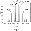
- a frequency comb, S 2 is generated as shown in Fig. 2 and graphically, over a range of drive frequencies, in Fig. 3 .
- resonator 40 may be characterized as a non-linear resonator element which forms a non-linear resonator oscillator (NLXO).
- a slope greater than 1 is an improvement in terms of making the output frequency of a selected tooth less dependent on the drive frequency f D than just using the drive frequency f D as a clock.
- the far-out phase noise is determined by the electronic noise in the sustaining circuit. This noise will not be present on the modes of resonator not used within a sustaining; thus, by locking a second VCXO (VCXO2) to a selected one (an n th tooth) of these teeth within a PLL and using the error signal of the PLL to correct for relative changes in frequency between VCXO (VCXO2) and S 2 , the output frequency of second VCXO (VCXO2) can be stabilized to a level provided by the n th tooth of the comb.
- VCXO2 Using a feedback tuning signal to the varactor in VCXO (1), one can tune the frequency of the drive signal S1 to the highest slope and lowest noise condition.
- the output frequency of second VCXO (VCXO2) might well be stabilized to a level provided by the first tooth to the left of the frequency of the drive oscillator (f D ) at a frequency in the range of 100.1658 - 100.1666 MHz because the slope (its first derivative) of the drive frequency vs. the comb frequency of this tooth in that range is 2.96.
- the slope is even steeper (closer to infinite) when the drive oscillator (f D ) is in a frequency in the range of 100.1660 - 100.1662 MHz Ideally, the slope (its first derivative) of the drive frequency vs.
- the comb frequency should be as large as possible (and the slope is infinite when the comb frequency response depicted by Fig. 3 is exactly vertical).
- the "Undetermined"region is due to the fact that the slope was too large to make a slope calculation with the equipment used for these measurements.
- the slope of the drive frequency f D is not surprisingly equal to +1. It is angled slightly to the left in Fig. 3 . As the slopes of the teeth get closer to absolutely vertical (moving in a clock-wise direction on Fig. 3 from fo) they approach an infinite slope (where the tooth frequency is desirously independent of the drive frequency). As the slope of the teeth move past vertical (again rotating in a clock-wise direction), the slope values become negative. So long as the slope of a selected tooth has an absolute value greater than one, it is has a desirable lower dependency on the drive frequency f D . If the slope of a selected tooth increases still further, that results in a further improvement in terms of being insensitive to the drive frequency.
- the scales of the Drive Frequency is very narrow compared to the scale of the Measured Comb Frequency of Fig. 3 , so a slope of 1 (of f D ) is close to, but not quite, vertical in this graph.
- the slopes of the teeth can have either positive or negative values. Since ideally the absolute value of the first derivative of the drive frequency versus the frequency of a tooth in the comb should have value greater than 1 (and preferably much greater than 1 and, even more preferably, infinite), operating the clock of Fig.
- VCXO1 first VCXO
- VCXO1 the embodiment of Fig. 1
- this noise will not be present in resonator 40.
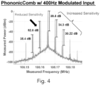
- the large slope region (left side of the comb in Fig. 3 ) of a comb will tend to filter out the electronic noise.
- the above design can be implemented in a quartz MEMS process in which VCXO (1), resonator (1), resonator (2), and VCXO (2) are all integrated with the PLL on a common semiconductor (Si, for example) substrate using quartz piezoelectric resonators.
- This will provide a chip-scale oscillator with dimensions of roughly ⁇ 20 mm 3 (a single quartz MEMS TCXO has been demonstrated with dimensions of 2 x 3 mm 2 , see R. L. Kubena, et al., "A Fully Integrated Quartz MEMS VHF TCXO," 2017 IEEE Frequency Control Symposium, Besancon, Fr., pp. 68 - 71, July 2017 ).
- quartz resonators have demonstrated high-Q combs with these unique features, other MEMS resonators formed of materials such as Si or AlN could be utilized instead so as long as they demonstrate the desired nonlinear and modal coupling effects.
- this application discloses at least the following: A method and apparatus for enhancing the stability of an oscillator circuit by generating a comb of frequencies in a non-linear resonator member in response to a drive frequency, the oscillator circuit including a voltage controlled oscillator which is locked to a particular tooth of the comb of frequencies produced by the non-linear resonator member at a drive frequency for which the absolute value of the first derivative of the drive frequency versus said comb frequency is greater than 1, and wherein the second voltage controlled oscillator is coupled with a phase locked loop circuit which controls the locking of the second voltage controlled oscillator to said particular tooth of the comb of frequencies.
Landscapes
- Physics & Mathematics (AREA)
- Nonlinear Science (AREA)
- General Physics & Mathematics (AREA)
- Optics & Photonics (AREA)
- Acoustics & Sound (AREA)
- Oscillators With Electromechanical Resonators (AREA)
Claims (12)
- Oscillateur comprenant : un premier oscillateur commandé en tension (VCXO1), un élément résonateur non linéaire (40), un second oscillateur commandé en tension (VCXO2) et un circuit à boucle à verrouillage de phase (50) ; le premier oscillateur commandé en tension (VCXO1) comprenant au moins un premier résonateur (30) et son circuit de maintien, le premier oscillateur (VCXO1) amenant l'élément résonateur non linéaire (40) à produire, lors de l'utilisation, un peigne de fréquences (S2), le second oscillateur commandé en tension (VCXO2) étant verrouillé, lors de l'utilisation, à une dent sélectionnée du peigne (S2) à une fréquence à laquelle la première dérivée de la fréquence d'attaque par rapport à la fréquence de la dent sélectionnée dans le peigne (S2) a une valeur absolue supérieure à 1, et le circuit à boucle à verrouillage de phase (50) commandant le verrouillage du deuxième oscillateur commandé en tension (VCXO2) à ladite fréquence de la dent sélectionnée.
- Oscillateur selon la revendication 1, les résonateurs (30, 40) comprenant chacun un élément résonant piézoélectrique en quartz.
- Oscillateur selon la revendication 1, le second oscillateur commandé en tension (VCXO2) étant verrouillé à une dent particulière du peigne (S2) à une fréquence à laquelle la première dérivée de la fréquence d'attaque par rapport à la fréquence du peigne (S2) a une valeur absolue supérieure à 2,5.
- Oscillateur selon la revendication 1, ledit élément résonateur non linéaire (40) et ledit premier résonateur (20) étant respectivement un troisième et un premier résonateur d'une pluralité de résonateurs piézoélectriques ; le circuit de maintien du premier oscillateur commandé en tension (VCXO1) formant un premier circuit de maintien couplé au premier (30) de la pluralité de résonateurs piézoélectriques, le second oscillateur commandé en tension (VCXO2) comprenant un second circuit de maintien couplé à un second de la pluralité de résonateurs piézoélectriques, le premier des circuits de maintien générant un signal d'attaque (S1) de fréquence donnée qui est appliqué audit troisième (40) de ladite pluralité de résonateurs piézoélectriques qui génère ledit signal de peigne de fréquence (S2) ; le second des circuits de maintien étant couplé à un système de boucle à verrouillage de phase (50) ; et le système de boucle à verrouillage de phase (50) commandant le verrouillage du second oscillateur (VCXO2) à la dent sélectionnée du peigne (S2), ladite première dérivée ayant une valeur absolue supérieure à un.
- Oscillateur selon la revendication 4, les résonateurs (30, 40) comprenant chacun un élément résonant piézoélectrique en quartz.
- Oscillateur selon la revendication 4, ladite dent particulière du peigne (S2) ayant une fréquence à laquelle la première dérivée de la fréquence d'attaque par rapport à la fréquence de peigne a une valeur absolue supérieure à 2,5.
- Procédé permettant d'améliorer la stabilité d'un circuit oscillateur en générant un peigne de fréquences dans un élément résonateur non linéaire (40) en réponse à une fréquence d'attaque (S1) générée par un premier oscillateur commandé en tension (VCXO1) doté d'un premier circuit de maintien, le circuit oscillateur comprenant en outre un second oscillateur commandé en tension (VCXO2) qui est verrouillé à une dent particulière ou sélectionnée du peigne (S2) de fréquences produites par l'élément résonateur non linéaire (40) à une fréquence d'attaque pour laquelle une valeur absolue de la première dérivée de la fréquence d'attaque (S1) par rapport à ladite fréquence de peigne est supérieure à 1, le second oscillateur commandé en tension (VCXO2) étant couplé à un circuit à boucle à verrouillage de phase (50) pour commander le verrouillage du second oscillateur commandé en tension (VCXO2) à ladite dent particulière ou sélectionnée du peigne de fréquences (S2).
- Procédé selon la revendication 7, l'élément résonateur non linéaire (40) comprenant un élément piézoélectrique en quartz.
- Procédé selon la revendication 7, le second oscillateur commandé en tension (VCXO2) comprenant un élément résonant constitué de quartz.
- Procédé selon la revendication 7, le second oscillateur commandé en tension (VCXO2) étant verrouillé à la dent particulière ou sélectionnée du peigne (S2) à une fréquence pour laquelle la première dérivée de la fréquence d'attaque (S1) par rapport à la fréquence de peigne est supérieure à 2,5.
- Procédé selon la revendication 7, le second oscillateur commandé en tension (VCXO2) comprenant un élément résonateur et l'élément résonateur inclus dans l'oscillateur commandé en tension (VCXO2) et l'élément résonateur non linéaire (40) comprenant chacun un élément piézoélectrique en quartz.
- Procédé selon la revendication 11, les deux éléments résonateurs étant thermostatés pour améliorer la stabilité des dents du peigne par rapport à la température.
Applications Claiming Priority (3)
| Application Number | Priority Date | Filing Date | Title |
|---|---|---|---|
| US201962904052P | 2019-09-23 | 2019-09-23 | |
| US16/932,455 US11156897B2 (en) | 2019-09-23 | 2020-07-17 | Enhanced stability oscillators using a phononic comb |
| PCT/US2020/051863 WO2021061575A1 (fr) | 2019-09-23 | 2020-09-21 | Oscillateurs à stabilité améliorée utilisant un peigne phononique |
Publications (3)
| Publication Number | Publication Date |
|---|---|
| EP4035263A1 EP4035263A1 (fr) | 2022-08-03 |
| EP4035263A4 EP4035263A4 (fr) | 2023-10-25 |
| EP4035263B1 true EP4035263B1 (fr) | 2025-01-22 |
Family
ID=74882321
Family Applications (1)
| Application Number | Title | Priority Date | Filing Date |
|---|---|---|---|
| EP20867516.5A Active EP4035263B1 (fr) | 2019-09-23 | 2020-09-21 | Oscillateurs à stabilité améliorée utilisant un peigne phononique |
Country Status (4)
| Country | Link |
|---|---|
| US (1) | US11156897B2 (fr) |
| EP (1) | EP4035263B1 (fr) |
| CN (1) | CN114788171B (fr) |
| WO (1) | WO2021061575A1 (fr) |
Families Citing this family (13)
| Publication number | Priority date | Publication date | Assignee | Title |
|---|---|---|---|---|
| US11988727B1 (en) | 2019-07-31 | 2024-05-21 | Hrl Laboratories, Llc | Magnetostrictive MEMS magnetic gradiometer |
| US11567147B1 (en) | 2019-07-31 | 2023-01-31 | Hrl Laboratories, Llc | Phononic comb enhanced gradiometers |
| US11747512B1 (en) | 2019-08-23 | 2023-09-05 | Hrl Laboratories, Llc | Phononic comb enhanced MEMS gravity gradiometers |
| US11575348B1 (en) | 2020-08-26 | 2023-02-07 | Hrl Laboratories, Llc | Phononic comb enhanced capacitive inductive sensor |
| US11431293B1 (en) | 2020-09-25 | 2022-08-30 | Hrl Laboratories, Llc | Noise suppression in a phononic comb |
| US11863194B1 (en) | 2021-02-02 | 2024-01-02 | Hrl Laboratories, Llc | Phononic comb enhanced atomic clock |
| US11606098B1 (en) | 2021-02-23 | 2023-03-14 | Hrl Laboratories, Llc | Comb enhanced oscillator with AM-to-PM noise suppression |
| US12483224B1 (en) * | 2021-07-16 | 2025-11-25 | Hrl Laboratories, Llc | Acoustically coupled dual resonators for phononic frequency comb generation |
| US11469738B1 (en) * | 2021-07-19 | 2022-10-11 | Txc Corporation | Oscillating device |
| US11699990B2 (en) | 2021-07-19 | 2023-07-11 | Txc Corporation | Oscillating device |
| US12160240B2 (en) * | 2022-07-29 | 2024-12-03 | Hrl Laboratories, Llc | Method and system for generating phononic frequency comb |
| US12191867B1 (en) | 2022-09-08 | 2025-01-07 | Hrl Laboratories, Llc | In-situ phase noise compensation for phononic frequency combs |
| CN120074510B (zh) * | 2024-12-26 | 2025-10-14 | 南京师范大学 | 一种磁控声子频率梳及其产生装置和方法 |
Family Cites Families (20)
| Publication number | Priority date | Publication date | Assignee | Title |
|---|---|---|---|---|
| US4132964A (en) * | 1977-07-28 | 1979-01-02 | National Semiconductor Corporation | Non-linearity correction in wide range voltage controlled oscillators |
| AU2003272195A1 (en) | 2002-04-30 | 2004-01-06 | Hrl Laboratories, Llc | Quartz-based nanoresonators and method of fabricating same |
| US20040190907A1 (en) * | 2003-03-25 | 2004-09-30 | General Instrument Corporation | All-optical reference clock for generating stable RF comb spectrum |
| KR20080044977A (ko) | 2006-11-17 | 2008-05-22 | 삼성전자주식회사 | 위상 동기 루프 및 위상 동기 루프의 동작 방법 |
| WO2009098686A2 (fr) * | 2008-02-07 | 2009-08-13 | Lahav Gan | Dispositif, système, et procédé de génération de fréquence utilisant un résonateur atomique |
| US7647688B1 (en) | 2008-08-11 | 2010-01-19 | Hrl Laboratories, Llc | Method of fabricating a low frequency quartz resonator |
| US8765615B1 (en) | 2010-06-15 | 2014-07-01 | Hrl Laboratories, Llc | Quartz-based MEMS resonators and methods of fabricating same |
| KR101255231B1 (ko) | 2011-05-30 | 2013-04-16 | 주식회사 브로던 | 콤제너레이터를 이용한 위상고정 발진기 |
| EP2730032B1 (fr) * | 2011-07-06 | 2021-04-14 | HRL Laboratories, LLC | Circuit d'accord automatique |
| US8601607B2 (en) * | 2011-09-22 | 2013-12-03 | Los Alamos National Security, Llc | Generation of a frequency comb and applications thereof |
| US9097656B2 (en) * | 2012-03-29 | 2015-08-04 | Imra America, Inc. | Methods for precision optical frequency synthesis and molecular detection |
| US8994465B1 (en) * | 2012-07-12 | 2015-03-31 | Hrl Laboratories, Llc | Phase noise reduction control loop for oscillators using nonlinear resonator operation |
| WO2014018444A2 (fr) | 2012-07-23 | 2014-01-30 | Associated Universities, Inc | Procédé de synthétiseur utilisant des raies de peigne de fréquences variables et un basculement de fréquence |
| CN103633537B (zh) * | 2013-11-13 | 2016-09-14 | 中国科学院物理研究所 | 一种载波包络相移频率可控的低噪声光纤激光频率梳装置 |
| US10110198B1 (en) | 2015-12-17 | 2018-10-23 | Hrl Laboratories, Llc | Integrated quartz MEMS tuning fork resonator/oscillator |
| US10389392B1 (en) | 2016-11-03 | 2019-08-20 | Hrl Laboratories, Llc | High-Q quartz-based inductor array for antenna matching |
| KR101811209B1 (ko) | 2016-12-06 | 2017-12-22 | 재단법인 막스플랑크 한국포스텍연구소 | 주파수 빗 및 나노플라즈모닉스 기술을 이용한 광자 발생기 및 광자 발생 방법 |
| US10921360B2 (en) | 2018-02-09 | 2021-02-16 | Hrl Laboratories, Llc | Dual magnetic and electric field quartz sensor |
| WO2019217668A1 (fr) * | 2018-05-09 | 2019-11-14 | Georgia Tech Research Corporation | Peignes de fréquence mécanique à résonance piézoélectrique |
| CN109586679B (zh) * | 2018-11-21 | 2021-11-16 | 电子科技大学 | 一种压电谐振器等效电参数及谐振频率的测量方法 |
-
2020
- 2020-07-17 US US16/932,455 patent/US11156897B2/en active Active
- 2020-09-21 CN CN202080064390.2A patent/CN114788171B/zh active Active
- 2020-09-21 EP EP20867516.5A patent/EP4035263B1/fr active Active
- 2020-09-21 WO PCT/US2020/051863 patent/WO2021061575A1/fr not_active Ceased
Also Published As
| Publication number | Publication date |
|---|---|
| EP4035263A4 (fr) | 2023-10-25 |
| US20210091748A1 (en) | 2021-03-25 |
| US11156897B2 (en) | 2021-10-26 |
| CN114788171A (zh) | 2022-07-22 |
| WO2021061575A1 (fr) | 2021-04-01 |
| CN114788171B (zh) | 2025-08-05 |
| EP4035263A1 (fr) | 2022-08-03 |
Similar Documents
| Publication | Publication Date | Title |
|---|---|---|
| EP4035263B1 (fr) | Oscillateurs à stabilité améliorée utilisant un peigne phononique | |
| US7982550B1 (en) | Highly accurate temperature stable clock based on differential frequency discrimination of oscillators | |
| CN105322960B (zh) | 使用自激振荡器的时钟发生器及其方法 | |
| EP1762004B1 (fr) | Synthetiseur de frequences | |
| US8446222B2 (en) | Apparatus and methods for reducing noise in oscillating signals | |
| US11431293B1 (en) | Noise suppression in a phononic comb | |
| Miller et al. | Phase control of self-excited parametric resonators | |
| TWI388128B (zh) | 用於單片式時脈產生器及時序/頻率參考器之頻率控制器 | |
| US8847695B2 (en) | Method, system and apparatus for accurate and stable LC-based reference oscillators | |
| Mussi et al. | A MEMS real-time clock with single-temperature calibration and deterministic jitter cancellation | |
| US8890591B1 (en) | Circuit and method of using time-average-frequency direct period syntheszier for improving crystal-less frequency generator frequency stability | |
| US7492195B1 (en) | Agile, low phase noise clock synthesizer and jitter attenuator | |
| CN109428549B (zh) | 拍频高q谐振器振荡器 | |
| CN111095797B (zh) | 用于低功率低相位噪声振荡器的自注入锁定 | |
| Xiu | A novel DCXO module for clock synchronization in MPEG2 transport system | |
| US11863194B1 (en) | Phononic comb enhanced atomic clock | |
| US11601089B1 (en) | BAW oscillators with dual BAW temperature sensing | |
| US7911283B1 (en) | Low noise oscillator and method | |
| WO1991007016A1 (fr) | Boucle a verrouillage de phase servant a produire une porteuse de reference pour un detecteur coherent | |
| US20100073096A1 (en) | Micro electro-mechanical system based programmable frequency synthesizer and method of operation thereof | |
| Rohde et al. | Noise minimization techniques for voltage controlled crystal oscillator (VCXO) circuits | |
| Shin et al. | A 21.4% tuning range 13 GHz quadrature voltage-controlled oscillator utilizing manipulatable inherent bimodal oscillation phenomenon in standard 90-nm CMOS process | |
| Rohde et al. | Voltage controlled crystal oscillator | |
| Daugey et al. | A HBAR-oscillator-based 4.596~ GHz frequency source: Application to a coherent population trapping Cs vapor cell atomic clock | |
| Boudot et al. | Characterization of high-overtone bulk acoustic resonators: applications to ultra-low noise microwave oscillators and miniature atomic clocks |
Legal Events
| Date | Code | Title | Description |
|---|---|---|---|
| STAA | Information on the status of an ep patent application or granted ep patent |
Free format text: STATUS: THE INTERNATIONAL PUBLICATION HAS BEEN MADE |
|
| PUAI | Public reference made under article 153(3) epc to a published international application that has entered the european phase |
Free format text: ORIGINAL CODE: 0009012 |
|
| STAA | Information on the status of an ep patent application or granted ep patent |
Free format text: STATUS: REQUEST FOR EXAMINATION WAS MADE |
|
| 17P | Request for examination filed |
Effective date: 20220412 |
|
| AK | Designated contracting states |
Kind code of ref document: A1 Designated state(s): AL AT BE BG CH CY CZ DE DK EE ES FI FR GB GR HR HU IE IS IT LI LT LU LV MC MK MT NL NO PL PT RO RS SE SI SK SM TR |
|
| DAV | Request for validation of the european patent (deleted) | ||
| DAX | Request for extension of the european patent (deleted) | ||
| A4 | Supplementary search report drawn up and despatched |
Effective date: 20230927 |
|
| RIC1 | Information provided on ipc code assigned before grant |
Ipc: H03L 7/16 20060101ALI20230921BHEP Ipc: G04F 5/14 20060101ALI20230921BHEP Ipc: G02B 5/00 20060101ALI20230921BHEP Ipc: G01N 21/552 20140101ALI20230921BHEP Ipc: H03L 7/099 20060101ALI20230921BHEP Ipc: H03B 5/32 20060101AFI20230921BHEP |
|
| GRAP | Despatch of communication of intention to grant a patent |
Free format text: ORIGINAL CODE: EPIDOSNIGR1 |
|
| STAA | Information on the status of an ep patent application or granted ep patent |
Free format text: STATUS: GRANT OF PATENT IS INTENDED |
|
| GRAS | Grant fee paid |
Free format text: ORIGINAL CODE: EPIDOSNIGR3 |
|
| INTG | Intention to grant announced |
Effective date: 20241015 |
|
| P01 | Opt-out of the competence of the unified patent court (upc) registered |
Free format text: CASE NUMBER: APP_60495/2024 Effective date: 20241110 |
|
| GRAA | (expected) grant |
Free format text: ORIGINAL CODE: 0009210 |
|
| STAA | Information on the status of an ep patent application or granted ep patent |
Free format text: STATUS: THE PATENT HAS BEEN GRANTED |
|
| AK | Designated contracting states |
Kind code of ref document: B1 Designated state(s): AL AT BE BG CH CY CZ DE DK EE ES FI FR GB GR HR HU IE IS IT LI LT LU LV MC MK MT NL NO PL PT RO RS SE SI SK SM TR |
|
| REG | Reference to a national code |
Ref country code: GB Ref legal event code: FG4D |
|
| REG | Reference to a national code |
Ref country code: CH Ref legal event code: EP |
|
| REG | Reference to a national code |
Ref country code: IE Ref legal event code: FG4D |
|
| REG | Reference to a national code |
Ref country code: DE Ref legal event code: R096 Ref document number: 602020045310 Country of ref document: DE |
|
| REG | Reference to a national code |
Ref country code: NL Ref legal event code: MP Effective date: 20250122 |
|
| PG25 | Lapsed in a contracting state [announced via postgrant information from national office to epo] |
Ref country code: NL Free format text: LAPSE BECAUSE OF FAILURE TO SUBMIT A TRANSLATION OF THE DESCRIPTION OR TO PAY THE FEE WITHIN THE PRESCRIBED TIME-LIMIT Effective date: 20250122 |
|
| PG25 | Lapsed in a contracting state [announced via postgrant information from national office to epo] |
Ref country code: RS Free format text: LAPSE BECAUSE OF FAILURE TO SUBMIT A TRANSLATION OF THE DESCRIPTION OR TO PAY THE FEE WITHIN THE PRESCRIBED TIME-LIMIT Effective date: 20250422 |
|
| PG25 | Lapsed in a contracting state [announced via postgrant information from national office to epo] |
Ref country code: FI Free format text: LAPSE BECAUSE OF FAILURE TO SUBMIT A TRANSLATION OF THE DESCRIPTION OR TO PAY THE FEE WITHIN THE PRESCRIBED TIME-LIMIT Effective date: 20250122 |
|
| PG25 | Lapsed in a contracting state [announced via postgrant information from national office to epo] |
Ref country code: PL Free format text: LAPSE BECAUSE OF FAILURE TO SUBMIT A TRANSLATION OF THE DESCRIPTION OR TO PAY THE FEE WITHIN THE PRESCRIBED TIME-LIMIT Effective date: 20250122 |
|
| PG25 | Lapsed in a contracting state [announced via postgrant information from national office to epo] |
Ref country code: ES Free format text: LAPSE BECAUSE OF FAILURE TO SUBMIT A TRANSLATION OF THE DESCRIPTION OR TO PAY THE FEE WITHIN THE PRESCRIBED TIME-LIMIT Effective date: 20250122 |
|
| REG | Reference to a national code |
Ref country code: LT Ref legal event code: MG9D |
|
| PG25 | Lapsed in a contracting state [announced via postgrant information from national office to epo] |
Ref country code: IS Free format text: LAPSE BECAUSE OF FAILURE TO SUBMIT A TRANSLATION OF THE DESCRIPTION OR TO PAY THE FEE WITHIN THE PRESCRIBED TIME-LIMIT Effective date: 20250522 Ref country code: NO Free format text: LAPSE BECAUSE OF FAILURE TO SUBMIT A TRANSLATION OF THE DESCRIPTION OR TO PAY THE FEE WITHIN THE PRESCRIBED TIME-LIMIT Effective date: 20250422 |
|
| REG | Reference to a national code |
Ref country code: AT Ref legal event code: MK05 Ref document number: 1762222 Country of ref document: AT Kind code of ref document: T Effective date: 20250122 |
|
| PG25 | Lapsed in a contracting state [announced via postgrant information from national office to epo] |
Ref country code: HR Free format text: LAPSE BECAUSE OF FAILURE TO SUBMIT A TRANSLATION OF THE DESCRIPTION OR TO PAY THE FEE WITHIN THE PRESCRIBED TIME-LIMIT Effective date: 20250122 |
|
| PG25 | Lapsed in a contracting state [announced via postgrant information from national office to epo] |
Ref country code: LV Free format text: LAPSE BECAUSE OF FAILURE TO SUBMIT A TRANSLATION OF THE DESCRIPTION OR TO PAY THE FEE WITHIN THE PRESCRIBED TIME-LIMIT Effective date: 20250122 Ref country code: PT Free format text: LAPSE BECAUSE OF FAILURE TO SUBMIT A TRANSLATION OF THE DESCRIPTION OR TO PAY THE FEE WITHIN THE PRESCRIBED TIME-LIMIT Effective date: 20250522 |
|
| PG25 | Lapsed in a contracting state [announced via postgrant information from national office to epo] |
Ref country code: BG Free format text: LAPSE BECAUSE OF FAILURE TO SUBMIT A TRANSLATION OF THE DESCRIPTION OR TO PAY THE FEE WITHIN THE PRESCRIBED TIME-LIMIT Effective date: 20250122 Ref country code: GR Free format text: LAPSE BECAUSE OF FAILURE TO SUBMIT A TRANSLATION OF THE DESCRIPTION OR TO PAY THE FEE WITHIN THE PRESCRIBED TIME-LIMIT Effective date: 20250423 |
|
| PG25 | Lapsed in a contracting state [announced via postgrant information from national office to epo] |
Ref country code: AT Free format text: LAPSE BECAUSE OF FAILURE TO SUBMIT A TRANSLATION OF THE DESCRIPTION OR TO PAY THE FEE WITHIN THE PRESCRIBED TIME-LIMIT Effective date: 20250122 |
|
| PG25 | Lapsed in a contracting state [announced via postgrant information from national office to epo] |
Ref country code: SE Free format text: LAPSE BECAUSE OF FAILURE TO SUBMIT A TRANSLATION OF THE DESCRIPTION OR TO PAY THE FEE WITHIN THE PRESCRIBED TIME-LIMIT Effective date: 20250122 |
|
| PG25 | Lapsed in a contracting state [announced via postgrant information from national office to epo] |
Ref country code: SM Free format text: LAPSE BECAUSE OF FAILURE TO SUBMIT A TRANSLATION OF THE DESCRIPTION OR TO PAY THE FEE WITHIN THE PRESCRIBED TIME-LIMIT Effective date: 20250122 |
|
| PG25 | Lapsed in a contracting state [announced via postgrant information from national office to epo] |
Ref country code: DK Free format text: LAPSE BECAUSE OF FAILURE TO SUBMIT A TRANSLATION OF THE DESCRIPTION OR TO PAY THE FEE WITHIN THE PRESCRIBED TIME-LIMIT Effective date: 20250122 |
|
| PGFP | Annual fee paid to national office [announced via postgrant information from national office to epo] |
Ref country code: DE Payment date: 20250929 Year of fee payment: 6 |
|
| PG25 | Lapsed in a contracting state [announced via postgrant information from national office to epo] |
Ref country code: IT Free format text: LAPSE BECAUSE OF FAILURE TO SUBMIT A TRANSLATION OF THE DESCRIPTION OR TO PAY THE FEE WITHIN THE PRESCRIBED TIME-LIMIT Effective date: 20250122 |
|
| PG25 | Lapsed in a contracting state [announced via postgrant information from national office to epo] |
Ref country code: CZ Free format text: LAPSE BECAUSE OF FAILURE TO SUBMIT A TRANSLATION OF THE DESCRIPTION OR TO PAY THE FEE WITHIN THE PRESCRIBED TIME-LIMIT Effective date: 20250122 Ref country code: EE Free format text: LAPSE BECAUSE OF FAILURE TO SUBMIT A TRANSLATION OF THE DESCRIPTION OR TO PAY THE FEE WITHIN THE PRESCRIBED TIME-LIMIT Effective date: 20250122 |
|
| REG | Reference to a national code |
Ref country code: DE Ref legal event code: R097 Ref document number: 602020045310 Country of ref document: DE |
|
| PG25 | Lapsed in a contracting state [announced via postgrant information from national office to epo] |
Ref country code: RO Free format text: LAPSE BECAUSE OF FAILURE TO SUBMIT A TRANSLATION OF THE DESCRIPTION OR TO PAY THE FEE WITHIN THE PRESCRIBED TIME-LIMIT Effective date: 20250122 |
|
| PG25 | Lapsed in a contracting state [announced via postgrant information from national office to epo] |
Ref country code: SK Free format text: LAPSE BECAUSE OF FAILURE TO SUBMIT A TRANSLATION OF THE DESCRIPTION OR TO PAY THE FEE WITHIN THE PRESCRIBED TIME-LIMIT Effective date: 20250122 |
|
| PLBE | No opposition filed within time limit |
Free format text: ORIGINAL CODE: 0009261 |
|
| STAA | Information on the status of an ep patent application or granted ep patent |
Free format text: STATUS: NO OPPOSITION FILED WITHIN TIME LIMIT |
|
| 26N | No opposition filed |
Effective date: 20251023 |