EP4052390B1 - Optischer drahtloser kommunikationsempfänger mit grosser fotodetektoroberfläche, grossem gesichtsfeld und hoher bandbreite - Google Patents
Optischer drahtloser kommunikationsempfänger mit grosser fotodetektoroberfläche, grossem gesichtsfeld und hoher bandbreite Download PDFInfo
- Publication number
- EP4052390B1 EP4052390B1 EP20801187.4A EP20801187A EP4052390B1 EP 4052390 B1 EP4052390 B1 EP 4052390B1 EP 20801187 A EP20801187 A EP 20801187A EP 4052390 B1 EP4052390 B1 EP 4052390B1
- Authority
- EP
- European Patent Office
- Prior art keywords
- photodiodes
- owc
- receiver
- wireless communication
- dimensional array
- Prior art date
- Legal status (The legal status is an assumption and is not a legal conclusion. Google has not performed a legal analysis and makes no representation as to the accuracy of the status listed.)
- Active
Links
Images


Classifications
-
- H—ELECTRICITY
- H04—ELECTRIC COMMUNICATION TECHNIQUE
- H04B—TRANSMISSION
- H04B10/00—Transmission systems employing electromagnetic waves other than radio-waves, e.g. infrared, visible or ultraviolet light, or employing corpuscular radiation, e.g. quantum communication
- H04B10/11—Arrangements specific to free-space transmission, i.e. transmission through air or vacuum
-
- H—ELECTRICITY
- H04—ELECTRIC COMMUNICATION TECHNIQUE
- H04B—TRANSMISSION
- H04B10/00—Transmission systems employing electromagnetic waves other than radio-waves, e.g. infrared, visible or ultraviolet light, or employing corpuscular radiation, e.g. quantum communication
- H04B10/60—Receivers
- H04B10/66—Non-coherent receivers, e.g. using direct detection
- H04B10/67—Optical arrangements in the receiver
Definitions
- the present invention relates generally to optical wireless communications, and more in particular to an optical wireless communication receiver having a large photodetector surface area and a high bandwidth.
- Optical Wireless Communication is a form of optical communication in which unguided visible, infrared (IR), or ultraviolet (UV) light is used to carry a signal, as for example shown in US 2016/294472 A1 , which discloses an optical wireless communication receiver with a lens and a plurality of detectors.
- OWC is quickly gaining interest in industry since the spectrum of (visible) light (with a wavelength range of about 400-700 nm) offers no less than 320 THz of bandwidth, and the spectrum commonly used in long-reach fibre optical communication (1500-1600 nm) about 12.5 THz, both much larger than even the upcoming THz radio technologies can offer.
- OWC can be used, among others, in a wide range of applications including wireless local area networks, wireless personal area networks and vehicular networks.
- the OWC systems that operate in the visible band are commonly referred to as Visible Light Communication, VLC, systems.
- the communicated data is modulated by pulsing the visible light at high speeds without noticeable effect on the lighting output and the human eye.
- VLC systems can be piggy-backed on LED illumination systems, as the LED's output light may not only serve illumination purposes but the LED may also be modulated with data, although with limited bandwidth as the LED is basically not designed for that.
- the OWC systems that operate in the Infra-Red, IR, and near-IR band offer a protocol-transparent link with high data rates.
- Such OWC systems use infrared beams which each can be directed on-demand to user devices. In this way, individual wireless links can be established to those devices with very high congestion-free capacity and high privacy as these beams are not shared and cannot be accessed by users which are not within the beam's footprint.
- OWC systems have a lot of advantages over RF based communication systems. As indicated, OWC systems have huge bandwidth potential, but moreover, the optical spectrum is unregulated and unlicensed. Since light cannot penetrate walls, OWC systems provide enhanced privacy and security.
- OWC systems also have several technical challenges, such as the challenge to efficiently steer the optical narrow beams individually and the challenge of how to align the optical receiver at the user device without the need of delicate accurate alignment efforts. Such delicate and accurate alignment would complicate the user's device and thus lead to increased costs.
- an Optical Wireless Communication, OWC, receiver for receiving an incoming optical beam modulated with data and outputting an output signal comprising the modulated data, the receiver comprising:
- an OWC receiver having a lens and a plurality of photodiodes which are positioned at a distance from the lens such that they are located at or closely to (i.e. preferably before) the focal plane of that lens.
- the inventor has found that when the interconnections of the photodiodes of the two-dimensional array (MxK) are configured as a matrix to form at least two parallel branches ( 1 ... K , wherein K ⁇ 2 ) of photodiodes, and wherein each of the parallel branches comprises a cascade (1...M, , wherein K ⁇ 2 ) of at least two photodiodes, a receiver is obtained of which the photodetector surface and bandwidth are configurable by definition of the interconnections which define the number of parallel branches and the number of cascaded photodiodes per branch.
- the proposed OWC receiver is arranged to receive an incoming optical beam which is modulated with high-speed data, and converts this to an electrical output signal.
- the OWC receiver deploys a photodiode which is followed by an electrical amplifier, in particular a transimpedance amplifier, which converts the summed photocurrents into the amplifier's output signal.
- the diameter of the beam is typically much larger than the active area of the photodiode, so to maximize the output signal the photodiode should capture as much as possible power of the incoming beam.
- the optical beam is captured by a lens first, and then projected onto the photodiode.
- an OWC receiver is proposed with a large cross-sectional aperture, as well as a wide field-of-view (FoV, i.e. large angular range). Since the photodetection area is formed by several individual photodiodes jointly, the individual active photodetection areas are small, which is typically required for an OWC receiver with a large bandwidth.
- FoV field-of-view
- Each photodiode of the array may be represented by an equivalent electrical circuit which consists of a (typically large) resistance which accounts for the leakage current, a capacitance of the reverse-biased photodiode junction, a current source of the (typically small) dark current generated by thermal effects, and a current source representing the photocurrent itself as a response to the fraction of the optical beam impinging on the active area of the photodiode.
- an OWC receiver is obtained in which the bandwidth and active area are configurable by adjusting the number of rows and columns of the array.
- the lens projects the received optical beam onto a surface area which is larger than the combined surface area of the two-dimensional array of photodiodes.
- the two-dimensional array of the photodiodes defining the rows and the columns of the two-dimensional array comprises interconnections of the photodiodes wherein respective interconnections defining each column (1...M) are also interconnections defining the rows ( 1...K ).
- each of the rows of the two-dimensional array further comprises a resistor positioned in parallel over the photodiodes of the respective row.
- each of the resistors is positioned outside of the two-dimensional array of the photodiodes.
- each of the resistors is integrated inside of the two-dimensional array of the photodiodes.
- an Optical Wireless Communication, OWC, system which comprises a receiver or a plurality of receivers according to any of the previous descriptions.
- the OWC system is adapted to provide optical communication via electromagnetic radiation with a wavelength in any one of the visible light spectrum, infrared light spectrum, near infrared light spectrum or ultraviolet light spectrum.
- the Optical Wireless Communication, OWC, system comprises one or more receivers according to any of the previous claims 1-9, wherein said OWC system is adapted for application in any one of a wireless local area network, wireless personal area network, and a vehicular network.
- the proposed OWC receiver receives the incoming optical beam that is modulated with the high-speed data, and converts this to an electrical output signal.
- the OWC receiver deploys a photodiode (PD in Fig. 1 ) which is followed by an electrical amplifier.
- the diameter of the optical beam is typically much larger than the active area of the photodiode, so to maximize the output signal the photodiode should capture as much as possible power of the incoming beam.
- the optical beam is captured by a lens first, and then projected onto the photodiode.
- the OWC receiver should have a large cross-sectional aperture, as well as a wide Field-of-View (FoV, i.e. large angular range). But to handle high data speeds, the OWC receiver should also have a large bandwidth, which typically requires a photodiode with a small active photodetection area.
- FoV Field-of-View
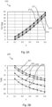
- the FoV's half angle ⁇ is increased when defocusing is applied, with a diameter D 2 of the photodiode of 0.2mm as indicated by reference 211, a diameter of 0.4mm as indicated by reference 212, a diameter of 0.8mm as indicated by reference 213, and a diameter of 1.0mm as indicated by reference 211.
- the FoV decreases slightly when the photodiode diameter is increased; on the other hand, the photodetected power increases considerably, as shown in Fig. 2B .
- Fig. 2A the FoV's half angle ⁇ is increased when defocusing is applied, with a diameter D 2 of the photodiode of 0.2mm as indicated by reference 211, a diameter of 0.4mm as indicated by reference 212, a diameter of 0.8mm as indicated by reference 213, and a diameter of 1.0mm as indicated by reference 211.
- the FoV decreases slightly when the photodiode diameter is increased; on the other hand, the photodetected power increases considerably, as shown in Fig
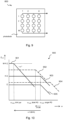
- Fig. 3 (left) describes the electrical circuit equivalent of a single photodiode, with serial resistance R s , parallel resistance R d , capacitance C d , dark current i d (t), and photo-current i s (t).
- a p-i-n photodiode is typically biased by a reverse voltage across its intrinsic region, and when photons penetrate into this region electron-hole pairs are generated which due to the electric field travel to the anode and cathode electrodes of the photodiode, respectively, and thus generate the photocurrent i s (t).
- the (typically small) serial resistance R s includes the bonding wires to the photodiode chip, the (high) parallel resistance R d includes the leakage current, and the (small) dark current i d (t) is generated by thermal effects.
- the photodiode can be represented by an equivalent circuit with a voltage source e(t) and serial impedance Z, and alternatively by applying Norton's theorem as shown in Fig.
- an electronic high-frequency low-noise amplifier is applied after the photodiode.
- N photodiodes can be put in parallel.
- the circuit model of such parallel arrangement is shown in Fig. 5 .
- Z T A ⁇ Z t 1 + A + N ⁇ Z t / R d 1 + j ⁇ R d C d + R s ⁇ A ⁇ Z t 1 + A + j ⁇ ⁇ N ⁇ C d Z t for R s ⁇ R d and R d ⁇ 1
- the output signal generated by the receiver with the N photodiodes in parallel is N times larger than that of the receiver with a single photodiode, but the receiver's bandwidth is N times smaller.
- the active area can be extended by putting N identical photodiodes in series.
- the equivalent circuit of such cascade of photodiodes is shown in Fig. 6 .
- Applying the equivalent voltage source circuit of the single photodiode in Fig. 3 (middle), this cascade is represented by Fig. 6 (left), where the n -th photodiode receives a fraction a n of the beam's power P (t), hence its photocurrent is i s,n (t) a n ⁇ R ⁇ P(t), and according to Thevenin can be represented again (similar as in Fig. 3 (middle)) as a voltage source e n (t) with serial impedance Z .
- Fig. 6 Applying the equivalent voltage source circuit of the single photodiode in Fig. 3 (middle), this cascade is represented by Fig. 6 (left), where the n -th photodiode receives a fraction a n of the beam's
- I on is the photodiode's dark current, R n photodiode responsivity, P n incident optical power on photodiode n (note that R n ⁇ P n ⁇ I n ⁇ R n ⁇ P n + I on ; at room temperature, kT / q » 25mV).
- Fig. 7 shows putting N photodiodes in series and applying the bias voltage V b across the whole series.
- a resistance R d in parallel and resistance R s in series with the photodiode has been included (in accordance with Fig. 3 ).
- V n N ⁇ I ⁇ R s + R d ⁇ N ⁇ R d I 0 n ⁇ + a n R n ⁇ ⁇ P
- V b N ⁇ R d I 0 n ⁇ + a n R n ⁇ ⁇ P N ⁇ R s + R d
- V n R d V b + N ⁇ R d I 0 n ⁇ + a n R n ⁇ ⁇ P N ⁇ R s + R d ⁇ I 0 n ⁇ a n R n ⁇ P
- V n R d R d + R s ⁇ V b N + R d 2 R d + R s I 0 n ⁇ + a n R n ⁇ ⁇ P ⁇ R d I 0 n + a n R n ⁇ P
- R d >> R s V n ⁇ V b N + R d I 0 n ⁇ ⁇ I 0 n + a n R n ⁇ ⁇ P ⁇ a n R n ⁇ P for R d ⁇ R s
- the total bias voltage V b is equally divided among the N photodiodes, yielding a bias voltage V b / N for each photodiode, where per photodiode n a bias voltage deviation can occur which is the product of its parallel resistance R d and the difference of the individual dark current I on and the individual generated photocurrent R n ⁇ P n with respect to the average values of these currents.
- R d parallel resistance
- the individual bias voltage deviation resulting from these differences can be reduced (if that is needed for adequate performance).
- the generated photocurrent is K times the current generated in each series of connected photodiodes; of each series, the current is equal to the average current generated in a single photodiode.
Landscapes
- Physics & Mathematics (AREA)
- Electromagnetism (AREA)
- Engineering & Computer Science (AREA)
- Computer Networks & Wireless Communication (AREA)
- Signal Processing (AREA)
- Optical Communication System (AREA)
- Light Receiving Elements (AREA)
Claims (13)
- Optischer Drahtloskommunikationsempfänger, OWC-Empfänger, (100) zum Empfangen eines eingehenden optischen Strahls, der mit Daten moduliert ist, und Ausgeben eines elektrischen Ausgangssignals, das die modulierten Daten umfasst, wobei der Empfänger umfasst:- eine Linse, die zum Empfangen des eingehenden optischen Strahls eingerichtet ist;- eine Vielzahl von Photodioden, die mit einem Abstand von der Linse positioniert sind und an oder proximal zu der Brennebene der Linse positioniert sind, wobei jede der Vielzahl von Photodioden zum Empfangen eines Bruchteils des eingehenden optischen Strahls und zum Erzeugen eines Photostroms (I11...IMK) entsprechend Photonen, die vom Bruchteil des eingehenden optischen Strahls empfangen werden, eingerichtet ist, wobei die Vielzahl von Photodioden (N) in einem zweidimensionalen Array (710, 800) (N=MxK) angeordnet ist, das Zeilen (1...M) und Spalten (1...K) umfasst, dadurch gekennzeichnet, dass die Ausgänge der Spalten (1 ... K) so kombiniert werden, dass ihre Photoströme summiert werden;- einen Verstärker, der mit kombinierten Ausgängen der Spalten (1 ... K) des zweidimensionalen Arrays verbunden ist und zum Umwandeln der summierten Photoströme in das Ausgangssignal des Verstärkers eingerichtet ist;wobei Zwischenverbindungen der Photodioden des zweidimensionalen Arrays (MxK) dazu ausgelegt sind, mindestens zwei parallele Spalten (1...K, wobei K≥2) von Photodioden zu bilden, und wobei jede der parallelen Spalten eine Kaskade (1...M, wobei K≥2) von mindestens zwei Photodioden umfasst, die eine kombinierte Photodetektorfläche bilden.
- Optischer Drahtloskommunikationsempfänger, OWC-Empfänger, (100) nach Anspruch 1, wobei die Anzahl paralleler Spalten (1...K) des zweidimensionalen Arrays (N=MxK) größer ist als die Anzahl kaskadierter (1...M) Photodioden, die in jeder der Spalten enthalten sind (M<K).
- Drahtloskommunikationsempfänger, OWC-Empfänger, (100) nach Anspruch 1, wobei die Anzahl paralleler Spalten (1...K) des zweidimensionalen Arrays (N=MxK) kleiner ist als die Anzahl kaskadierter (1...M) Photodioden, die in jeder der Spalten enthalten sind (M>K).
- Drahtloskommunikationsempfänger, OWC-Empfänger, (100) nach Anspruch 1, wobei die Anzahl paralleler Spalten (1...K) des zweidimensionalen Arrays (N=MxK) gleich der Anzahl kaskadierter (1...M) Photodioden ist, die in jeder der Spalten enthalten sind (M=K).
- Drahtloskommunikationsempfänger, OWC-Empfänger, (100) nach einem der vorstehenden Ansprüche, wobei die Linse den empfangenen optischen Strahl auf eine Oberflächenfläche projiziert, die größer als die kombinierte Oberflächenfläche des zweidimensionalen Arrays von Photodioden ist.
- Drahtloskommunikationsempfänger, OWC-Empfänger, (100) nach einem der vorstehenden Ansprüche, wobei das zweidimensionale Array von Photodioden, die die Zeilen und die Spalten des zweidimensionalen Arrays (N=MxK) definieren, Zwischenverbindungen der Photodioden umfasst, wobei jeweilige Zwischenverbindungen, die jede Spalte (1...M) definieren, auch Zwischenverbindungen sind, die die Zeilen (1 ... K) definieren.
- Drahtloskommunikationsempfänger, OWC-Empfänger, (100) nach einem der vorstehenden Ansprüche, wobei jede der Zeilen des zweidimensionalen Arrays ferner einen Widerstand umfasst, der parallel über die Photodioden der jeweiligen Zeile positioniert ist.
- Optischer Drahtloskommunikationsempfänger, OWC-Empfänger, (100) nach Anspruch 7, wobei jeder der Widerstände außerhalb des zweidimensionalen Arrays der Photodioden positioniert ist.
- Optischer Drahtloskommunikationsempfänger, OWC-Empfänger, (100) nach Anspruch 7, wobei jeder der Widerstände innerhalb des zweidimensionalen Arrays der Photodioden integriert ist.
- Optisches Drahtloskommunikationssystem, OWC-System, das einen Empfänger (100) nach einem der vorstehenden Ansprüche umfasst.
- Optisches Drahtloskommunikationssystem, OWC-System, nach Anspruch 10, das eine Vielzahl von Empfängern (100) nach einem der vorstehenden Ansprüche 1-9 umfasst.
- Optisches Drahtloskommunikationssystem, OWC-System, das einen oder mehrere Empfänger (100) nach einem der vorstehenden Ansprüche 1-9 umfasst, wobei das OWC-System dazu ausgebildet ist, eine optische Kommunikation mittels elektromagnetischer Strahlung mit einer Wellenlänge in einem beliebigen des Spektrums von sichtbarem Licht, des Infrarotlichtspektrums, des Nahinfrarotlichtspektrums oder des Ultraviolettlichtspektrums bereitzustellen.
- Optisches Drahtloskommunikationssystem, OWC-System, das einen oder mehrere Empfänger (100) nach einem der vorstehenden Ansprüche 1-9 umfasst, wobei das OWC-System zur Anwendung in einem beliebigen eines drahtlosen Lokalnetzwerks, eines drahtlosen persönlichen Netzwerks und eines Fahrzeugnetzwerks ausgebildet ist.
Applications Claiming Priority (2)
| Application Number | Priority Date | Filing Date | Title |
|---|---|---|---|
| US201962928625P | 2019-10-31 | 2019-10-31 | |
| PCT/EP2020/080594 WO2021084108A1 (en) | 2019-10-31 | 2020-10-30 | An optical wireless communication receiver with large photodetector surface area, large field of view and high bandwidth |
Publications (2)
| Publication Number | Publication Date |
|---|---|
| EP4052390A1 EP4052390A1 (de) | 2022-09-07 |
| EP4052390B1 true EP4052390B1 (de) | 2024-10-23 |
Family
ID=73131701
Family Applications (1)
| Application Number | Title | Priority Date | Filing Date |
|---|---|---|---|
| EP20801187.4A Active EP4052390B1 (de) | 2019-10-31 | 2020-10-30 | Optischer drahtloser kommunikationsempfänger mit grosser fotodetektoroberfläche, grossem gesichtsfeld und hoher bandbreite |
Country Status (6)
| Country | Link |
|---|---|
| US (1) | US11923900B2 (de) |
| EP (1) | EP4052390B1 (de) |
| JP (1) | JP7651568B2 (de) |
| ES (1) | ES3009709T3 (de) |
| FI (1) | FI4052390T3 (de) |
| WO (1) | WO2021084108A1 (de) |
Families Citing this family (2)
| Publication number | Priority date | Publication date | Assignee | Title |
|---|---|---|---|---|
| US12088118B2 (en) * | 2020-05-12 | 2024-09-10 | King Abdullah University Of Science And Technology | Energy-autonomous optical wireless communication system |
| CN114300489A (zh) * | 2021-12-28 | 2022-04-08 | 网络通信与安全紫金山实验室 | 一种光电探测器装置、设计方法及无线光通信系统 |
Family Cites Families (10)
| Publication number | Priority date | Publication date | Assignee | Title |
|---|---|---|---|---|
| US5311353A (en) | 1993-03-05 | 1994-05-10 | Analog Modules | Wide dynamic range optical receivers |
| DE10213045B4 (de) * | 2002-03-22 | 2004-05-06 | Melexis Gmbh | Integrierter optischer Faser-Empfänger |
| US7230227B2 (en) * | 2004-10-08 | 2007-06-12 | The Boeing Company | Lenslet/detector array assembly for high data rate optical communications |
| KR100853186B1 (ko) | 2006-12-05 | 2008-08-20 | 한국전자통신연구원 | 다중 개구면 광검출기 및 그 광검출기를 포함한 광신호검출회로 |
| JP4856757B2 (ja) | 2007-03-16 | 2012-01-18 | 富士通セミコンダクター株式会社 | 光受信装置、および受信方法 |
| KR20090047615A (ko) * | 2007-11-08 | 2009-05-13 | 삼성전자주식회사 | 가시광 통신 시스템에서 가시광 신호 수신 방법 및 장치 |
| JPWO2010134154A1 (ja) | 2009-05-18 | 2012-11-08 | 株式会社日立製作所 | 光通信システムおよび光通信方法 |
| JP5271838B2 (ja) | 2009-07-30 | 2013-08-21 | 浜松ホトニクス株式会社 | 点滅信号検出装置 |
| KR20160110432A (ko) | 2014-01-10 | 2016-09-21 | 팔머 랩스, 엘엘씨 | 발산-광선 통신 시스템 |
| US10756815B2 (en) * | 2017-08-24 | 2020-08-25 | Molex, Llc | Free space optical data transmission using photodetector array |
-
2020
- 2020-10-30 EP EP20801187.4A patent/EP4052390B1/de active Active
- 2020-10-30 WO PCT/EP2020/080594 patent/WO2021084108A1/en not_active Ceased
- 2020-10-30 ES ES20801187T patent/ES3009709T3/es active Active
- 2020-10-30 FI FIEP20801187.4T patent/FI4052390T3/fi active
- 2020-10-30 JP JP2022525797A patent/JP7651568B2/ja active Active
- 2020-10-30 US US17/773,457 patent/US11923900B2/en active Active
Also Published As
| Publication number | Publication date |
|---|---|
| JP2023500499A (ja) | 2023-01-06 |
| WO2021084108A1 (en) | 2021-05-06 |
| ES3009709T3 (en) | 2025-03-31 |
| JP7651568B2 (ja) | 2025-03-26 |
| US11923900B2 (en) | 2024-03-05 |
| FI4052390T3 (fi) | 2025-01-29 |
| EP4052390A1 (de) | 2022-09-07 |
| US20220393759A1 (en) | 2022-12-08 |
Similar Documents
| Publication | Publication Date | Title |
|---|---|---|
| Koonen et al. | Novel broadband OWC receiver with large aperture and wide field-of-view | |
| US11196486B2 (en) | Array-based free-space optical communication links | |
| US7230227B2 (en) | Lenslet/detector array assembly for high data rate optical communications | |
| US10965379B2 (en) | Coherent receiver for free space optical communications and lidar | |
| Koonen et al. | Beam-steered optical wireless communication for industry 4.0 | |
| US20030090765A1 (en) | Free-space optical communication system | |
| US20020171896A1 (en) | Free-space optical communication system employing wavelength conversion | |
| EP4052390B1 (de) | Optischer drahtloser kommunikationsempfänger mit grosser fotodetektoroberfläche, grossem gesichtsfeld und hoher bandbreite | |
| JP2004512730A (ja) | 光ワイヤレス通信の改善または関連する改善 | |
| Jungnickel et al. | Electronic tracking for wireless infrared communications | |
| KR20200122367A (ko) | 다중 채널의 확산-빔 광학 무선 통신을 위한 시스템 | |
| Koonen et al. | Optical wireless GbE receiver with large field-of-view | |
| Sarbazi et al. | Design tradeoffs of non-imaging angle diversity receivers for 6G optical wireless access networks | |
| Soltani et al. | Optimal imaging receiver design for high-speed mobile optical wireless communications | |
| Ferraro et al. | 2.5 G large area avalanche photodiodes for free space optical communication | |
| Sarbazi et al. | Imaging angle diversity receiver design for 6G optical wireless communications: performance tradeoffs and optimisation | |
| Zhou et al. | Robust wide-angle optical wireless communication system: From design to prototype | |
| GB2565199A (en) | Optical detector | |
| US12199668B2 (en) | Receiving system for high speed and large coverage optical wireless communication | |
| Sarbazi et al. | A robust and compact non-imaging angle diversity receiver for 6G optical wireless communications | |
| Liang et al. | Transparent optical wireless hubs using wavelength space division multiplexing | |
| US20240319006A1 (en) | Serial array of modulators and detectors | |
| GB2565201A (en) | Concentrator height reduction | |
| US20250175256A1 (en) | Optical receiving apparatus | |
| O'Brien | Improving coverage and data rate in optical wireless systems |
Legal Events
| Date | Code | Title | Description |
|---|---|---|---|
| STAA | Information on the status of an ep patent application or granted ep patent |
Free format text: STATUS: UNKNOWN |
|
| STAA | Information on the status of an ep patent application or granted ep patent |
Free format text: STATUS: THE INTERNATIONAL PUBLICATION HAS BEEN MADE |
|
| PUAI | Public reference made under article 153(3) epc to a published international application that has entered the european phase |
Free format text: ORIGINAL CODE: 0009012 |
|
| STAA | Information on the status of an ep patent application or granted ep patent |
Free format text: STATUS: REQUEST FOR EXAMINATION WAS MADE |
|
| 17P | Request for examination filed |
Effective date: 20220426 |
|
| AK | Designated contracting states |
Kind code of ref document: A1 Designated state(s): AL AT BE BG CH CY CZ DE DK EE ES FI FR GB GR HR HU IE IS IT LI LT LU LV MC MK MT NL NO PL PT RO RS SE SI SK SM TR |
|
| DAV | Request for validation of the european patent (deleted) | ||
| DAX | Request for extension of the european patent (deleted) | ||
| GRAP | Despatch of communication of intention to grant a patent |
Free format text: ORIGINAL CODE: EPIDOSNIGR1 |
|
| STAA | Information on the status of an ep patent application or granted ep patent |
Free format text: STATUS: GRANT OF PATENT IS INTENDED |
|
| RIC1 | Information provided on ipc code assigned before grant |
Ipc: H04B 10/67 20130101ALI20240425BHEP Ipc: H04B 10/11 20130101AFI20240425BHEP |
|
| INTG | Intention to grant announced |
Effective date: 20240514 |
|
| GRAS | Grant fee paid |
Free format text: ORIGINAL CODE: EPIDOSNIGR3 |
|
| GRAA | (expected) grant |
Free format text: ORIGINAL CODE: 0009210 |
|
| STAA | Information on the status of an ep patent application or granted ep patent |
Free format text: STATUS: THE PATENT HAS BEEN GRANTED |
|
| AK | Designated contracting states |
Kind code of ref document: B1 Designated state(s): AL AT BE BG CH CY CZ DE DK EE ES FI FR GB GR HR HU IE IS IT LI LT LU LV MC MK MT NL NO PL PT RO RS SE SI SK SM TR |
|
| REG | Reference to a national code |
Ref country code: GB Ref legal event code: FG4D |
|
| REG | Reference to a national code |
Ref country code: CH Ref legal event code: EP |
|
| REG | Reference to a national code |
Ref country code: DE Ref legal event code: R096 Ref document number: 602020039977 Country of ref document: DE |
|
| REG | Reference to a national code |
Ref country code: IE Ref legal event code: FG4D |
|
| REG | Reference to a national code |
Ref country code: FI Ref legal event code: FGE |
|
| REG | Reference to a national code |
Ref country code: NL Ref legal event code: FP |
|
| REG | Reference to a national code |
Ref country code: SE Ref legal event code: TRGR |
|
| REG | Reference to a national code |
Ref country code: LT Ref legal event code: MG9D |
|
| P01 | Opt-out of the competence of the unified patent court (upc) registered |
Free format text: CASE NUMBER: APP_4567/2025 Effective date: 20250128 |
|
| REG | Reference to a national code |
Ref country code: AT Ref legal event code: MK05 Ref document number: 1735697 Country of ref document: AT Kind code of ref document: T Effective date: 20241023 |
|
| REG | Reference to a national code |
Ref country code: ES Ref legal event code: FG2A Ref document number: 3009709 Country of ref document: ES Kind code of ref document: T3 Effective date: 20250331 |
|
| PG25 | Lapsed in a contracting state [announced via postgrant information from national office to epo] |
Ref country code: PT Free format text: LAPSE BECAUSE OF FAILURE TO SUBMIT A TRANSLATION OF THE DESCRIPTION OR TO PAY THE FEE WITHIN THE PRESCRIBED TIME-LIMIT Effective date: 20250224 Ref country code: HR Free format text: LAPSE BECAUSE OF FAILURE TO SUBMIT A TRANSLATION OF THE DESCRIPTION OR TO PAY THE FEE WITHIN THE PRESCRIBED TIME-LIMIT Effective date: 20241023 Ref country code: IS Free format text: LAPSE BECAUSE OF FAILURE TO SUBMIT A TRANSLATION OF THE DESCRIPTION OR TO PAY THE FEE WITHIN THE PRESCRIBED TIME-LIMIT Effective date: 20250223 |
|
| PG25 | Lapsed in a contracting state [announced via postgrant information from national office to epo] |
Ref country code: BG Free format text: LAPSE BECAUSE OF FAILURE TO SUBMIT A TRANSLATION OF THE DESCRIPTION OR TO PAY THE FEE WITHIN THE PRESCRIBED TIME-LIMIT Effective date: 20241023 |
|
| PG25 | Lapsed in a contracting state [announced via postgrant information from national office to epo] |
Ref country code: NO Free format text: LAPSE BECAUSE OF FAILURE TO SUBMIT A TRANSLATION OF THE DESCRIPTION OR TO PAY THE FEE WITHIN THE PRESCRIBED TIME-LIMIT Effective date: 20250123 |
|
| PG25 | Lapsed in a contracting state [announced via postgrant information from national office to epo] |
Ref country code: LV Free format text: LAPSE BECAUSE OF FAILURE TO SUBMIT A TRANSLATION OF THE DESCRIPTION OR TO PAY THE FEE WITHIN THE PRESCRIBED TIME-LIMIT Effective date: 20241023 Ref country code: AT Free format text: LAPSE BECAUSE OF FAILURE TO SUBMIT A TRANSLATION OF THE DESCRIPTION OR TO PAY THE FEE WITHIN THE PRESCRIBED TIME-LIMIT Effective date: 20241023 Ref country code: GR Free format text: LAPSE BECAUSE OF FAILURE TO SUBMIT A TRANSLATION OF THE DESCRIPTION OR TO PAY THE FEE WITHIN THE PRESCRIBED TIME-LIMIT Effective date: 20250124 |
|
| PG25 | Lapsed in a contracting state [announced via postgrant information from national office to epo] |
Ref country code: PL Free format text: LAPSE BECAUSE OF FAILURE TO SUBMIT A TRANSLATION OF THE DESCRIPTION OR TO PAY THE FEE WITHIN THE PRESCRIBED TIME-LIMIT Effective date: 20241023 |
|
| PG25 | Lapsed in a contracting state [announced via postgrant information from national office to epo] |
Ref country code: RS Free format text: LAPSE BECAUSE OF FAILURE TO SUBMIT A TRANSLATION OF THE DESCRIPTION OR TO PAY THE FEE WITHIN THE PRESCRIBED TIME-LIMIT Effective date: 20250123 |
|
| REG | Reference to a national code |
Ref country code: CH Ref legal event code: PL |
|
| PG25 | Lapsed in a contracting state [announced via postgrant information from national office to epo] |
Ref country code: SM Free format text: LAPSE BECAUSE OF FAILURE TO SUBMIT A TRANSLATION OF THE DESCRIPTION OR TO PAY THE FEE WITHIN THE PRESCRIBED TIME-LIMIT Effective date: 20241023 |
|
| PG25 | Lapsed in a contracting state [announced via postgrant information from national office to epo] |
Ref country code: MC Free format text: LAPSE BECAUSE OF FAILURE TO SUBMIT A TRANSLATION OF THE DESCRIPTION OR TO PAY THE FEE WITHIN THE PRESCRIBED TIME-LIMIT Effective date: 20241023 |
|
| PG25 | Lapsed in a contracting state [announced via postgrant information from national office to epo] |
Ref country code: DK Free format text: LAPSE BECAUSE OF FAILURE TO SUBMIT A TRANSLATION OF THE DESCRIPTION OR TO PAY THE FEE WITHIN THE PRESCRIBED TIME-LIMIT Effective date: 20241023 |
|
| PG25 | Lapsed in a contracting state [announced via postgrant information from national office to epo] |
Ref country code: LU Free format text: LAPSE BECAUSE OF NON-PAYMENT OF DUE FEES Effective date: 20241030 Ref country code: BE Free format text: LAPSE BECAUSE OF NON-PAYMENT OF DUE FEES Effective date: 20241031 |
|
| PG25 | Lapsed in a contracting state [announced via postgrant information from national office to epo] |
Ref country code: EE Free format text: LAPSE BECAUSE OF FAILURE TO SUBMIT A TRANSLATION OF THE DESCRIPTION OR TO PAY THE FEE WITHIN THE PRESCRIBED TIME-LIMIT Effective date: 20241023 |
|
| PG25 | Lapsed in a contracting state [announced via postgrant information from national office to epo] |
Ref country code: CH Free format text: LAPSE BECAUSE OF NON-PAYMENT OF DUE FEES Effective date: 20241031 |
|
| PG25 | Lapsed in a contracting state [announced via postgrant information from national office to epo] |
Ref country code: RO Free format text: LAPSE BECAUSE OF FAILURE TO SUBMIT A TRANSLATION OF THE DESCRIPTION OR TO PAY THE FEE WITHIN THE PRESCRIBED TIME-LIMIT Effective date: 20241023 |
|
| REG | Reference to a national code |
Ref country code: DE Ref legal event code: R097 Ref document number: 602020039977 Country of ref document: DE |
|
| PG25 | Lapsed in a contracting state [announced via postgrant information from national office to epo] |
Ref country code: SK Free format text: LAPSE BECAUSE OF FAILURE TO SUBMIT A TRANSLATION OF THE DESCRIPTION OR TO PAY THE FEE WITHIN THE PRESCRIBED TIME-LIMIT Effective date: 20241023 |
|
| PG25 | Lapsed in a contracting state [announced via postgrant information from national office to epo] |
Ref country code: CZ Free format text: LAPSE BECAUSE OF FAILURE TO SUBMIT A TRANSLATION OF THE DESCRIPTION OR TO PAY THE FEE WITHIN THE PRESCRIBED TIME-LIMIT Effective date: 20241023 |
|
| REG | Reference to a national code |
Ref country code: BE Ref legal event code: MM Effective date: 20241031 |
|
| PLBE | No opposition filed within time limit |
Free format text: ORIGINAL CODE: 0009261 |
|
| STAA | Information on the status of an ep patent application or granted ep patent |
Free format text: STATUS: NO OPPOSITION FILED WITHIN TIME LIMIT |
|
| 26N | No opposition filed |
Effective date: 20250724 |
|
| PG25 | Lapsed in a contracting state [announced via postgrant information from national office to epo] |
Ref country code: IE Free format text: LAPSE BECAUSE OF NON-PAYMENT OF DUE FEES Effective date: 20241030 |
|
| PGFP | Annual fee paid to national office [announced via postgrant information from national office to epo] |
Ref country code: NL Payment date: 20251030 Year of fee payment: 6 |
|
| PGFP | Annual fee paid to national office [announced via postgrant information from national office to epo] |
Ref country code: DE Payment date: 20251030 Year of fee payment: 6 |
|
| PGFP | Annual fee paid to national office [announced via postgrant information from national office to epo] |
Ref country code: GB Payment date: 20251030 Year of fee payment: 6 |
|
| PGFP | Annual fee paid to national office [announced via postgrant information from national office to epo] |
Ref country code: FI Payment date: 20251028 Year of fee payment: 6 Ref country code: IT Payment date: 20251030 Year of fee payment: 6 |
|
| PGFP | Annual fee paid to national office [announced via postgrant information from national office to epo] |
Ref country code: FR Payment date: 20251031 Year of fee payment: 6 |
|
| PGFP | Annual fee paid to national office [announced via postgrant information from national office to epo] |
Ref country code: SE Payment date: 20251030 Year of fee payment: 6 |
|
| PGFP | Annual fee paid to national office [announced via postgrant information from national office to epo] |
Ref country code: ES Payment date: 20251216 Year of fee payment: 6 |
|
| PG25 | Lapsed in a contracting state [announced via postgrant information from national office to epo] |
Ref country code: HU Free format text: LAPSE BECAUSE OF FAILURE TO SUBMIT A TRANSLATION OF THE DESCRIPTION OR TO PAY THE FEE WITHIN THE PRESCRIBED TIME-LIMIT; INVALID AB INITIO Effective date: 20201030 |
|
| PG25 | Lapsed in a contracting state [announced via postgrant information from national office to epo] |
Ref country code: CY Free format text: LAPSE BECAUSE OF FAILURE TO SUBMIT A TRANSLATION OF THE DESCRIPTION OR TO PAY THE FEE WITHIN THE PRESCRIBED TIME-LIMIT; INVALID AB INITIO Effective date: 20201030 |