EP4097766B1 - Dispositif de photo-détection à gradient latéral de concentration en cadmium dans la zone de charge d'espace - Google Patents
Dispositif de photo-détection à gradient latéral de concentration en cadmium dans la zone de charge d'espace Download PDFInfo
- Publication number
- EP4097766B1 EP4097766B1 EP21732380.7A EP21732380A EP4097766B1 EP 4097766 B1 EP4097766 B1 EP 4097766B1 EP 21732380 A EP21732380 A EP 21732380A EP 4097766 B1 EP4097766 B1 EP 4097766B1
- Authority
- EP
- European Patent Office
- Prior art keywords
- pixel
- cadmium
- doped region
- photo
- structured coating
- Prior art date
- Legal status (The legal status is an assumption and is not a legal conclusion. Google has not performed a legal analysis and makes no representation as to the accuracy of the status listed.)
- Active
Links
Images


Classifications
-
- H—ELECTRICITY
- H10—SEMICONDUCTOR DEVICES; ELECTRIC SOLID-STATE DEVICES NOT OTHERWISE PROVIDED FOR
- H10F—INORGANIC SEMICONDUCTOR DEVICES SENSITIVE TO INFRARED RADIATION, LIGHT, ELECTROMAGNETIC RADIATION OF SHORTER WAVELENGTH OR CORPUSCULAR RADIATION
- H10F30/00—Individual radiation-sensitive semiconductor devices in which radiation controls the flow of current through the devices, e.g. photodetectors
- H10F30/20—Individual radiation-sensitive semiconductor devices in which radiation controls the flow of current through the devices, e.g. photodetectors the devices having potential barriers, e.g. phototransistors
- H10F30/21—Individual radiation-sensitive semiconductor devices in which radiation controls the flow of current through the devices, e.g. photodetectors the devices having potential barriers, e.g. phototransistors the devices being sensitive to infrared, visible or ultraviolet radiation
- H10F30/22—Individual radiation-sensitive semiconductor devices in which radiation controls the flow of current through the devices, e.g. photodetectors the devices having potential barriers, e.g. phototransistors the devices being sensitive to infrared, visible or ultraviolet radiation the devices having only one potential barrier, e.g. photodiodes
- H10F30/221—Individual radiation-sensitive semiconductor devices in which radiation controls the flow of current through the devices, e.g. photodetectors the devices having potential barriers, e.g. phototransistors the devices being sensitive to infrared, visible or ultraviolet radiation the devices having only one potential barrier, e.g. photodiodes the potential barrier being a PN homojunction
- H10F30/2212—Individual radiation-sensitive semiconductor devices in which radiation controls the flow of current through the devices, e.g. photodetectors the devices having potential barriers, e.g. phototransistors the devices being sensitive to infrared, visible or ultraviolet radiation the devices having only one potential barrier, e.g. photodiodes the potential barrier being a PN homojunction the devices comprising active layers made of only Group II-VI materials, e.g. HgCdTe infrared photodiodes
-
- H—ELECTRICITY
- H10—SEMICONDUCTOR DEVICES; ELECTRIC SOLID-STATE DEVICES NOT OTHERWISE PROVIDED FOR
- H10F—INORGANIC SEMICONDUCTOR DEVICES SENSITIVE TO INFRARED RADIATION, LIGHT, ELECTROMAGNETIC RADIATION OF SHORTER WAVELENGTH OR CORPUSCULAR RADIATION
- H10F30/00—Individual radiation-sensitive semiconductor devices in which radiation controls the flow of current through the devices, e.g. photodetectors
- H10F30/20—Individual radiation-sensitive semiconductor devices in which radiation controls the flow of current through the devices, e.g. photodetectors the devices having potential barriers, e.g. phototransistors
- H10F30/21—Individual radiation-sensitive semiconductor devices in which radiation controls the flow of current through the devices, e.g. photodetectors the devices having potential barriers, e.g. phototransistors the devices being sensitive to infrared, visible or ultraviolet radiation
- H10F30/22—Individual radiation-sensitive semiconductor devices in which radiation controls the flow of current through the devices, e.g. photodetectors the devices having potential barriers, e.g. phototransistors the devices being sensitive to infrared, visible or ultraviolet radiation the devices having only one potential barrier, e.g. photodiodes
- H10F30/222—Individual radiation-sensitive semiconductor devices in which radiation controls the flow of current through the devices, e.g. photodetectors the devices having potential barriers, e.g. phototransistors the devices being sensitive to infrared, visible or ultraviolet radiation the devices having only one potential barrier, e.g. photodiodes the potential barrier being a PN heterojunction
-
- H—ELECTRICITY
- H10—SEMICONDUCTOR DEVICES; ELECTRIC SOLID-STATE DEVICES NOT OTHERWISE PROVIDED FOR
- H10F—INORGANIC SEMICONDUCTOR DEVICES SENSITIVE TO INFRARED RADIATION, LIGHT, ELECTROMAGNETIC RADIATION OF SHORTER WAVELENGTH OR CORPUSCULAR RADIATION
- H10F71/00—Manufacture or treatment of devices covered by this subclass
- H10F71/125—The active layers comprising only Group II-VI materials, e.g. CdS, ZnS or CdTe
- H10F71/1253—The active layers comprising only Group II-VI materials, e.g. CdS, ZnS or CdTe comprising at least three elements, e.g. HgCdTe
-
- H—ELECTRICITY
- H10—SEMICONDUCTOR DEVICES; ELECTRIC SOLID-STATE DEVICES NOT OTHERWISE PROVIDED FOR
- H10F—INORGANIC SEMICONDUCTOR DEVICES SENSITIVE TO INFRARED RADIATION, LIGHT, ELECTROMAGNETIC RADIATION OF SHORTER WAVELENGTH OR CORPUSCULAR RADIATION
- H10F77/00—Constructional details of devices covered by this subclass
- H10F77/10—Semiconductor bodies
- H10F77/12—Active materials
- H10F77/123—Active materials comprising only Group II-VI materials, e.g. CdS, ZnS or HgCdTe
- H10F77/1233—Active materials comprising only Group II-VI materials, e.g. CdS, ZnS or HgCdTe characterised by the dopants
-
- H—ELECTRICITY
- H10—SEMICONDUCTOR DEVICES; ELECTRIC SOLID-STATE DEVICES NOT OTHERWISE PROVIDED FOR
- H10F—INORGANIC SEMICONDUCTOR DEVICES SENSITIVE TO INFRARED RADIATION, LIGHT, ELECTROMAGNETIC RADIATION OF SHORTER WAVELENGTH OR CORPUSCULAR RADIATION
- H10F77/00—Constructional details of devices covered by this subclass
- H10F77/10—Semiconductor bodies
- H10F77/12—Active materials
- H10F77/123—Active materials comprising only Group II-VI materials, e.g. CdS, ZnS or HgCdTe
- H10F77/1237—Active materials comprising only Group II-VI materials, e.g. CdS, ZnS or HgCdTe having at least three elements, e.g. HgCdTe
-
- H—ELECTRICITY
- H10—SEMICONDUCTOR DEVICES; ELECTRIC SOLID-STATE DEVICES NOT OTHERWISE PROVIDED FOR
- H10F—INORGANIC SEMICONDUCTOR DEVICES SENSITIVE TO INFRARED RADIATION, LIGHT, ELECTROMAGNETIC RADIATION OF SHORTER WAVELENGTH OR CORPUSCULAR RADIATION
- H10F77/00—Constructional details of devices covered by this subclass
- H10F77/30—Coatings
- H10F77/306—Coatings for devices having potential barriers
Definitions
- the invention relates to the field of infrared photodiodes made of Cd x Hg 1-x Te (0 ⁇ x ⁇ 1), used to detect infrared radiation in particular for applications in infrared imaging.
- a photodiode comprises a substrate made of semiconductor material, in which a PN junction separates an N-doped region from a P-doped region. At thermodynamic equilibrium, a space charge zone, devoid of free carriers, extends on either side of the PN junction and induces an intense electric field in the photodiode.
- one of the N-doped region and the P-doped region forms an absorption region.
- a photon of suitable wavelength is absorbed in the absorption region, it creates a so-called minority carrier.
- This minority carrier diffuses in the substrate until reaching the space charge zone, where it is accelerated by the intense electric field towards the other doped region. It recombines in this other doped region by forming an electric current of carrier recombination.
- a photodiode is only sensitive in a specific wavelength range, which depends on the band gap, or gap, in the absorption region. A low value of the gap in the absorption region ensures sensitivity of the photodiode to long wavelengths.
- Dark current is an imperfection in photodiodes caused by thermal agitation that provides sufficient energy to form an electron-hole pair through spontaneous generation. If this electron-hole pair is formed in the charge zone of space, there is formation of an electric current of carrier recombination which does not correspond to photon absorption. A high gap value in the space charge region ensures reduced dark current.
- Cd x Hg 1-x Te photodiodes with an absorption region with a low cadmium content, so that the photodiode is sensitive to long wavelengths, and a serving with a high cadmium content.
- at least a portion of the space charge region extends into the high cadmium portion, thereby providing reduced dark current.
- An example of such a photodiode is described in the patent application WO 2013/079446 .
- the absorption region is N-doped.
- a box with a high cadmium content extends into the P-doped region, with a substantially constant cadmium concentration.
- the box is obtained by covering a Cd x Hg 1-x Te substrate with a cadmium-rich layer, and by carrying out an inter-diffusion anneal during which the cadmium atoms of the cadmium-rich layer will diffuse into the substrate, very preferably in the P-doped region.
- “rich in cadmium” means consisting of a material in which at least one atom in three is a cadmium atom, preferably one atom in two.
- a disadvantage of this solution is that it requires a compromise on the composition of the box, to prevent the latter from forming a potential barrier hindering the diffusion of minority carriers in the space charge zone. It is therefore necessary to ensure that the cadmium concentration in the box does not exceed a critical threshold beyond which the sensitivity of the photodiode is strongly affected. This results in the need for precise control of the annealing conditions, to avoid the diffusion of too large a quantity of cadmium towards the P-doped region.
- An objective of the present invention is to propose a photo-detection device based on Cd x Hg 1-x Te, which offers both sensitivity to long lengths wave and a reduced dark current, and which does not present the disadvantages of the prior art.
- Another objective of the present invention is to propose a method of manufacturing such a device.
- the concentration gradient in cadmium is a lateral gradient, that is to say a variation of the cadmium concentration in planes parallel to the plane of the substrate.
- Each pixel defines a photodiode.
- the P-doped region is shallow with regard to its lateral extent, with for example a ratio greater than or equal to three between its depth and its diameter.
- the lateral extent designates its maximum width, respectively its maximum length, both defined in a plane parallel to the plane of the substrate.
- the spectral sensitivity range is defined by the cadmium concentration in the N-doped region. This concentration is fixed freely, and so as to detect photons at the desired wavelengths, preferably in the infrared.
- each pixel includes a box with a higher concentration of cadmium, located only in the P-doped region, and named here “concentrated box”.
- the average gap in the concentrated box is therefore greater than the average gap in the N-doped region.
- the space charge zone extends at least partly in the concentrated box, which makes it possible to reduce the current. darkness.
- the concentrated box in each pixel, comprises at least one intermediate gap zone and at least one high gap zone.
- the space charge zone therefore extends partly in the intermediate gap zone, and partly in the high gap zone.
- the intermediate gap zone has an average cadmium concentration strictly lower than the average cadmium concentration in the high gap zone.
- the average gap in the intermediate gap zone is therefore lower than the average gap in the high gap zone.
- the intermediate gap zone is in direct physical contact with the electrical contact pad. For the collection of carriers to remain possible, it is therefore sufficient that the average gap in the intermediate gap zone does not form a potential barrier hindering the diffusion of minority carriers. It is not a problem, on the other hand, that the average gap in the high gap zone hinders the diffusion of minority carriers. In other words, the reduction of the dark current is ensured, at least, by the strong gap zone, while the collection of carriers is ensured, at least, by the intermediate gap zone.
- the average gap in the high gap zone can exceed a threshold limit beyond which it forms a potential barrier for the minority carriers, the average value of the gap in the concentrated box can be increased in comparison with the art prior. The dark current is therefore further reduced.
- the average gap in the intermediate gap zone can be low enough to ensure good collection of charge carriers whatever the operating conditions (temperatur, photon flux, etc.).
- the concentrated box is obtained simply by covering the substrate with a structured layer rich in cadmium and by carrying out inter-diffusion annealing. During this annealing, the cadmium atoms of the cadmium-rich structured layer will diffuse into the substrate, mainly in the P-doped region.
- the cadmium concentration gradient is obtained using one or more through opening(s). breakthrough(s) in the cadmium-rich structured layer.
- the structured coating may comprise several superimposed layers, including a sealing layer, distinct from the cadmium-rich layer and capable of blocking the passage of doping elements towards the interior of the semiconductor substrate.
- the photo-detection device advantageously comprises at least two pixels, and each pixel comprises the same number of through opening(s) in the structured coating, distributed in the same way on the pixel and having the same dimensions from one pixel to another.
- each intermediate gap zone is preferably surrounded laterally by at least part of the at least one high gap zone.
- the concentrated box may comprise a single intermediate gap zone and a single high gap zone, with the single intermediate gap zone laterally surrounded by the single high gap zone.
- the concentrated box may comprise a single intermediate gap zone and two high gap zones, with the intermediate gap zone which forms an open volume in the center and with the two high gap zones respectively. around and in the center of the intermediate gap zone.
- the concentrated box may comprise a plurality of intermediate gap zones, and a high gap zone which extends around and between the intermediate gap zones.
- the minimum cadmium concentration value in the concentrated box is strictly greater than the minimum cadmium concentration value in the N-doped region.
- the photo-detection device advantageously comprises a plurality of pixels which all have the same cut-off wavelength.
- the semiconductor substrate may have a mesa topology, with, in each pixel, a respective mesa pad receiving the P-doped region.
- the production of the PN junction advantageously comprises a step of injecting doping elements into the semiconductor substrate, this step being implemented after step a) and the doping elements being injected through the at least a through opening of the structured covering.
- the structured coating may comprise several superimposed layers, including a sealing layer, distinct from the cadmium-rich layer and capable of blocking the passage of doping elements towards the interior of the semiconductor substrate.
- the method further comprises, for each pixel, a step of producing the electrical contact pad implemented after test b), with the electrical contact pad which extends into each through opening of the structured coating in said pixel.
- an average cadmium concentration designates an average volume concentration of cadmium atoms.
- FIG. 1A illustrates, in a sectional view in a plane (yOz), a first embodiment of a photo-detection device 100 according to the invention.
- the photo-detection device 100 comprises a substrate 110 of semiconductor material, made of an alloy of cadmium, mercury and tellurium of the Cd x Hg 1-x Te type, with x between 0 and 1, terminals excluded.
- the substrate 110 here has two large faces parallel to the plane (xOy), which respectively define an upper face 111 and a lower face 112 of the substrate 110 (thin wafer type substrate).
- the substrate 110 is constituted here by an N-doped region 120, and at least one P-doped region 130.
- Each P-doped region 130 forms a respective PN 140 junction with the N-doped region 120.
- Each PN 140 junction defines a photodiode, and each photodiode corresponds to a respective pixel of the photo-detection device 100.
- the photo-detection device 100 comprises a single pixel.
- the N-doped region 120 forms a so-called absorption region, N-doped here with indium ions.
- photons incident on the photo-detection device 100 penetrate into the substrate 110, and form an electron-hole pair in the N-doped region 120.
- the P-doped region 130 is P-doped with acceptor doping elements preferably belonging to column V of the periodic table of elements, for example arsenic.
- the P-doped region 130 is flush with the upper face 111 of the substrate 110. It has a thin volume shape, with a reduced dimension along the axis (Oz) of the depth in the substrate 110 and large dimensions along the axes (Ox). and (Oy). Preferably, it has a depth at least ten times less than its diameter. Its depth can be between 100 nm and 1000 nm, for example equal to 200 nm. Its diameter can be between 1 ⁇ m and 25 ⁇ m, for example equal to 10 ⁇ m.
- the P 130 doped region consists of Cd x Hg 1-x Te, with x preferably between 0.15 and 0.95. The value of x is variable, depending on the location considered in the P 130 doped region.
- a concentrated box 150 is defined, located only inside the P-doped region.
- the concentrated box 150 extends inside the P-doped region 130, from the upper face 111 of the substrate 110 to a bottom of the box, on the side opposite to said upper face of the substrate.
- the bottom of the concentrated box is located substantially at the level of the PN junction 140, preferably less than 20 nm from the latter.
- the average concentration of cadmium in the concentrated box 150 is strictly greater than the average concentration of cadmium in the N-doped region 120.
- the average concentration of cadmium in the concentrated box 150 corresponds to a value V1 of x
- the average concentration of cadmium in the N-doped region corresponds to a V2 value of x
- V1 is strictly greater than V2.
- the concentrated box 150 presents a cadmium concentration gradient.
- the value taken by x varies along the axes (Ox) and (Oy), in the concentrated box 150 and in planes parallel to the upper face 111 of the substrate 110. Said gradient can therefore be called "lateral gradient".
- the value taken by x varies in the concentrated box 150 between a higher value x max and a lower value x min strictly less than x max .
- the upper value x max is preferably between 1.5 and 5 times V2 (average cadmium concentration in the N-doped region), or even between 1.5 and 3 times V2, while remaining less than unity.
- V2 average cadmium concentration in the N-doped region
- the lower value x min is greater than or equal to the minimum cadmium concentration in the N-doped region, preferably strictly greater than this minimum concentration.
- the minimum cadmium concentration in the N-doped region can be equal to V2, the average cadmium concentration in the N-doped region.
- x min must not exceed a threshold limit beyond which a barrier is formed. of potential blocking the diffusion of charge carriers (under normal operating conditions of the photodiode, when a bias voltage is applied to the latter).
- a ratio between x min and V2 is between 1.1 and 3, more preferably between 1.2 and 2.5.
- the cadmium concentration gradient makes it possible to define at least one so-called intermediate gap zone 151 and at least one so-called strong gap zone 152, which together constitute the concentrated box 150.
- Each strong gap zone 152 therefore has an average cadmium concentration which corresponds at a V3 value of x
- each intermediate gap zone 151 has an average cadmium concentration which corresponds to a V4 value of x
- V3 is strictly greater than V4.
- a ratio between V3 and V4 is between 1.2 and 5, preferably between 1.5 and 3.
- the concentrated box 150 is constituted by a single intermediate gap zone 151 and a single high gap zone 152, with the single intermediate gap zone 151 entirely surrounded laterally by the single strong gap zone 152.
- laterally surrounded means surrounded in planes parallel to the plane of the substrate.
- the substrate 110 also includes an intermediate zone 160, which here extends laterally (along the axes (Ox) and (Oy)) and vertically (along the axis (Oz)), between the edge of the concentrated box 150 and the junction PN 140.
- this intermediate zone the cadmium concentration decreases rapidly from a cadmium concentration at the edge of the concentrated box 150.
- the distance between the edge of the concentrated box 150 and the PN junction 140 defines an extent of the intermediate zone 160. This extended has a reduced value, preferably less than 200 nm.
- Such an intermediate zone 160 can extend on one side and/or the other of the PN junction 140, in the P-doped region and/or in the N-doped region.
- the intermediate zone occupies less than 10% of the volume of the P-doped region, and the concentrated box occupies more than 90% of the volume of the P-doped region.
- the concentrated box 150 extends over the entire volume of the P-doped region.
- the substrate 110 is covered, on the side of its upper face 111, by a structured coating 180 which extends directly on the substrate 110.
- the structured coating 180 comprises at least one through opening per pixel, here one and only through opening 181 in the pixel.
- Each pixel has as many through opening(s) as intermediate gap zone(s) in the concentrated box, each through opening being located opposite a respective intermediate gap zone of said box.
- the structured coating 180 comprises a cadmium-rich layer, consisting of an alloy comprising cadmium, for example CdTe, CdS, CdSe, CdZnSe, etc.
- This cadmium-rich layer extends directly on the substrate 110, in direct physical contact with the latter.
- the structured coating 180 consists of this single layer rich in cadmium.
- it may include other layers, in particular a sealing layer capable of blocking the passage of doping elements towards the interior of the substrate (see Figure 6 ).
- Each pixel also includes an electrical contact pad 170, in direct physical contact with each intermediate gap zone of the concentrated box belonging to the same pixel.
- the electrical contact pad 170 extends on the side of the upper face 111 of the substrate 110, penetrating into each through opening 181 of the structured coating to come into contact with the corresponding intermediate gap zone 151.
- the electrical contact pad 170 can cover all or part of the surface of the substrate left free by the latter. Preferably, the electrical contact pad 170 completely fills each through opening 181 of the structured coating in the pixel. In each through opening 181, the electrical contact pad 170 can rest against the upper face 111 of the substrate 110, or sink slightly into the intermediate gap zone. In addition, the electrical contact pad 170 can extend only inside the through opening 181, or extend to the top of the structured covering 180. When the pixel has several intermediate gap zones and several through openings, the electrical contact pad comprises contact portions located in said through openings and one or more connection portion(s) located between said through openings and on the top of the structured covering 180.
- each intermediate gap zone 151 of the concentrated box is therefore surmounted by a respective through opening 181 of the structured coating, and in direct physical contact with the electrical contact pad 170 through said through opening 181.
- the space charge zone extends on either side of the PN junction 140, partly in the concentrated box 150. Thanks to the higher average concentration of cadmium in the concentrated box 150, the device photodetector 100 can detect photons at long wavelengths while exhibiting reduced dark current. In each pixel, the collection of charge carriers is carried out at the level of at least one intermediate gap zone 151, connected to the electrical contact pad 170. Consequently, the possible presence of a potential barrier at the level of the strong gap zone 152 does not prevent efficient collection of charge carriers. We can therefore increase an average value of the gap in the space charge zone, in comparison with the prior art, and thus further reduce the dark current for the same range of spectral sensitivity. We can also relax the manufacturing tolerances, since the value of the gap is only a sensitive parameter in only part of the concentrated box.
- the intermediate gap zone corresponds to the portions of the concentrated box in which x is between x min and a threshold value strictly less than x max .
- the high gap zone then corresponds to the remainder of the concentrated box.
- the high gap zone can correspond to the portions of the concentrated box in which x is substantially equal to x max .
- the high gap zone then extends facing the solid portions of the structured coating, while each intermediate gap zone extends facing a respective through opening of the structured coating.
- the intermediate gap and high gap zones could be defined differently, for example so that the high gap zone also extends with regard to peripheral regions of the through openings.
- an overlapping surface between the P-doped region and the structured coating is non-zero. In an extreme case, this overlapping surface may be zero. In this case, the edges of the P-doped region can be directly adjacent to the edges of a through opening of the structured coating, at the level of the upper face 111 of the substrate 110. In any case, this covering surface is a surface between a minimum and a maximum, where this minimum can take the value zero, and where the maximum is advantageously equal to the surface of the P-doped region flush with the upper face of the substrate reduced by 0.5 ⁇ m 2 .
- FIGS. 2A, 2A' to 2C, 2C' schematically illustrate different variants of distribution of intermediate gap and high gap zones in a pixel of the device according to the invention.
- the intermediate gap and high gap zones are distributed as in the example of the Figure 1A .
- FIG. 2A is a sectional view of the pixel, in a plane (x0y) parallel to the plane of the substrate.
- Figure 2A' is a sectional view of the same pixel, in a plane (y0z) orthogonal to the plane of the substrate and passing through the axis ⁇ '.
- the concentrated box is constituted by a single intermediate gap zone 251A and a single high gap zone 252A.
- the intermediate gap zone 251A extends in the center of the concentrated box, entirely surrounded laterally by the strong gap zone 252A.
- the structured covering 280A has a single through opening, located opposite the intermediate gap zone 251A.
- the 270A electrical contact pad fills this single through opening. This variant makes it possible to limit the volume of the intermediate gap zone as much as possible, and ensures optimal collection of charge carriers and a minimum dark current.
- the concentrated box is made up of a single intermediate gap zone 251B and two high gap zones 252B.
- FIG 2B is a sectional view of the pixel, in a plane (x0y) parallel to the plane of the substrate.
- Figure 2B' is a sectional view of the same pixel, in a plane (y0z) orthogonal to the plane of the substrate and passing through the ⁇ ' axis.
- the intermediate gap zone 251B forms an open volume in the center, centered on the pixel.
- the strong gap zones 252B extend respectively inside and around this open volume in the center.
- the structured covering 280B comprises a single through opening, which surrounds a solid portion of the structured covering and which is located facing the intermediate gap zone 251B.
- the electrical contact pad 270B fills this single through opening.
- the collection of charge carriers takes place in the intermediate gap zone, at the periphery of the pixel. Counterintuitively, this positioning of the collection zones promotes a good modulation transfer function.
- the concentrated box is made up of four distinct intermediate gap zones 251C and a high gap zone 252C.
- FIG 2C is a sectional view of the pixel, in a plane (x0y) parallel to the plane of the substrate.
- Figure 2C' is a sectional view of the same pixel, in a plane (y0z) orthogonal to the plane of the substrate and passing through the axis ⁇ '.
- the intermediate gap zones 251C extend respectively to the four corners of the pixel.
- the strong gap zone 252C extends between and around the intermediate gap zones 251C.
- the structured covering 280C has four through openings, each facing a respective intermediate gap zone 251C.
- the 270C electrical contact pad fills these four through openings and covers also a structured covering part.
- This variant makes it possible to combine a good modulation transfer function and a minimal dark current, thanks to positioning of the intermediate gap zones on the periphery of the pixel and on a reduced volume.
- the pixel has a non-square shape, always with a respective intermediate gap zone at each corner of the pixel.
- the distribution of the through openings in the structured coating is similar to the distribution of the intermediate gap zones, with at least one through opening in each pixel of the photo-detection device.
- a through opening can surround a solid portion of the structured covering.
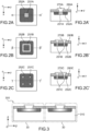
- FIG. 3 schematically illustrates a second mode of a photo-detection device 300 according to the invention, according to a sectional view in a plane (yOz).
- This second embodiment only differs from the first embodiment in that it comprises several pixels 30, sharing the same substrate 310. All the pixels 30 are surmounted by the same set of at least one through opening in the coating structure. In particular, each of the sets of at least one through opening comprises the same number of through opening(s), distributed in the same way over the pixel, with the same dimensions from one pixel to the next. 'other. All pixels 30 also have the same cut-off wavelength, with the same value of the minimum cadmium concentration in the N-doped region.
- the P-doped region has a substantially square section in a plane (x0y) parallel to the plane of the substrate.
- This example is not limiting, and numerous other forms of P-doped region can be implemented without departing from the scope of the present invention, for example a P-doped region of round or oval section in a plane (x0y) parallel to the plane of the substrate.
- the at least one through opening located facing the P-doped region, in the structured coating may have a section other than square, for example round or oval, in a plane (x0y) parallel to the plane of the substrate.
- the section of the through opening is preferably a homothesis of the section of the P-doped region.
- the invention is not limited to one or more pixels of square section in a plane (x0y) parallel to the plane of the substrate.
- an ion implantation of doping elements is carried out in a semiconductor substrate 410 made of Cd x Hg 1-x Te ( Figure 4A ).
- the substrate 410 initially has N-type doping over its entire volume, produced for example by indium ions.
- the doping elements implanted are of the acceptor type, for example arsenic or any other element belonging to column V of the periodic table of elements (phosphorus, antimony, bismuth, etc.).
- the implantation conditions are standard, for example an energy of 500 keV and an implantation dose of 2.10 15 atoms/cm 2 . We thus obtain an implantation zone 431 in the substrate 410.
- the doping elements are implanted in the substrate at the level of a so-called upper face of the latter.
- the structured coating here consists of CdTe, and includes at least one through opening 481.
- the structured coating 480 can be produced by deposition or epitaxy of a solid layer, then etching through an etching mask to form the at least one through opening 481.
- the etching can be chemical etching using 'a Bromine solution, in which the etching depth is adjusted by adjusting a duration of the chemical etching, or a selective chemical etching, in which the substrate 410 is not sensitive to etching, or an ionic type dry etch or plasma, etc.
- the engraving mask is typically made of resin.
- the structured coating 480 is produced using a resin mask, deposited directly on the substrate then covered with CdTe. When the resin mask is removed, the CdTe is removed at the same time except at the locations of the openings in the resin mask, which forms a structured CdTe layer on the substrate (lift-off technique).
- the substrate 410 is therefore constituted by a region 421, weakly P-doped due to the mercury vacancies, and at least one P-doped region 430, heavily P-doped thanks to the acceptor doping elements.
- the covering surface 482 between the P-doped region 430 and the solid portions of the structured coating 480 we identified the covering surface 482 between the P-doped region 430 and the solid portions of the structured coating 480.
- the diffusion of cadmium is an ionic, isotropic diffusion, with a diffusion length which involves an acceleration term due to the Fermi level.
- this term increases with the carrier density.
- this term takes the value 1, and therefore does not come into play.
- Cadmium therefore diffuses almost only in the P-doped region 430, where the carrier density is very high in comparison with the weakly P-doped region 421 (then N-doped following annealing under saturating pressure of mercury vapor, as described below with reference to the Figure 4E ). We are therefore talking about selective inter-diffusion.
- the cadmium diffuses into the substrate from the covering surface 482 between the P-doped region and the structured coating 480.
- a concentrated box with a lateral gradient of cadmium is therefore formed in the P-doped region 430.
- the concentrated box is automatically located in the P-doped region, thanks to the selective nature of the inter-diffusion of cadmium (the diffusion of cadmium towards the N-doped region exists, but it is negligible compared to the diffusion of cadmium towards the region doped P).
- the cadmium concentration is maximum with regard to the covering surface 482 between the P-doped region and the structured coating 480, then decreases with as one moves away from this covering surface 482.
- the lateral cadmium concentration gradient makes it possible to define at least one intermediate gap zone and at least one high gap zone in the concentrated box.
- the level of cadmium, and therefore the gap in the concentrated box is determined by the quantity of cadmium available in the structured coating, the dimensions of the covering surface between the P-doped region and the structured coating, and the heat balance associated with the inter-diffusion annealing (duration and temperature, defining cadmium diffusion lengths).
- the quantity of cadmium available in the structured coating and the dimensions of the covering surface define in particular a maximum gap level threshold in the concentrated box, which cannot under any circumstances be exceeded. This threshold effect also makes the gap gradient in the concentrated box very reproducible.
- it is possible to obtain a minimum gap in the concentrated box which is identical for all the pixels of the same photo-detection device, and from one photo-detection device to another. This ensures great homogeneity of detection performance, from one pixel to another of the same device, even for large devices with very many pixels. Likewise, we can ensure great homogeneity of detection performance, from one device to another.
- the level of cadmium in the concentrated box increases more slowly than if the annealing was carried out with a solid layer of CdTe.
- a rate of diffusion of cadmium atoms, from the structured coating towards the P-doped region is a function of the dimensions of the covering surface 482 between the structured coating 480 and the P-doped zone 430. It will therefore be easier to ensure that the gap in the intermediate gap zone does not exceed a limit threshold beyond which it forms a potential barrier for the charge carriers, since this limit threshold will be reached later, for a longer annealing duration significant and/or a higher annealing temperature.
- the manufacturing process is therefore particularly robust, thanks in particular to a relaxation of the constraints on the control of the conditions of inter-diffusion annealing.
- a new annealing is then carried out, under saturating pressure of mercury vapor ( Figure 4E ).
- This new annealing makes it possible to fill the mercury vacancies in region 421.
- region 421 has N doping and forms the N doped region 420 as described with reference to the Figure 1A .
- This new annealing is carried out at a temperature between 150°C and 350°C, for example 250°C.
- the electrical contact pad 470 is thus automatically aligned with the low gap zone, for the collection of charge carriers.
- the structured coating is advantageously preserved in the final device, to form a passivation layer.
- the same annealing performs at least two functions among the diffusion of the doping elements, the activation of the doping elements, the inter-diffusion of the cadmium, and the filling of the mercury vacancies.
- the method according to the invention requires only a reduced number of steps, without strong alignment constraints.
- the concentrated box is automatically located in the P-doped zone, and the electrical contact pad is automatically aligned with the intermediate gap zone of the concentrated box.
- the different anneals, and more particularly the inter-diffusion annealing, have no influence on the cut-off wavelength of the photo-detection device obtained in end of process. Indeed, the cadmium atoms of the structured coating hardly diffuse in the N-doped region, and if necessary remain localized near the upper face of the substrate.
- FIGS. 5A to 5E illustrate the steps of a second embodiment of the method according to the invention, which will only be described for its differences relative to the method of Figures 4A to 4B .
- the doping elements are injected into the substrate 510 using saturating pressure annealing of doping elements in the vapor phase.
- This annealing carries out the injection of the doping elements into the substrate, and their diffusion inside the substrate.
- this annealing also achieves the activation of the doping elements in the substrate.
- the activation of the doping elements is carried out by a separate annealing.
- the P-doped region 530 thus obtained is therefore automatically aligned with the through opening 581 of the structured coating 580.
- the P-doped region 530 is here slightly wider than the through opening 581, due to the diffusion of the doping elements in the substrate .
- This second embodiment offers automatic alignment of the through opening of the structured coating relative to the P-doped region, particularly advantageous for reduced pixel pitches (for example less than or equal to 10 ⁇ m, which is often the case in imaging infrared).
- doping by annealing under saturating pressure of doping elements in the vapor phase avoids the creation of defects in the substrate.
- FIGS. 8A and 8B illustrate the first steps of a third embodiment of the method according to the invention, which will only be described for its differences relative to the method of Figures 4A to 4B .
- a step in producing the structured coating 880 ( Figure 8A ) is implemented prior to the injection of the doping elements into the substrate 810 ( Figure 8B ), so as to achieve automatic alignment of each through opening of the structured coating with a respective P-doped region.
- the injection of doping elements is carried out by ionic injection.
- the following steps are not illustrated, and correspond to the steps of Figures 4C to 4F .
- the structured coating may include a layer impermeable to doping elements, or be only partially impervious to doping elements so that the P-doped region ultimately reproduces the topology of the structured coating.
- the photo-detection device has a planar configuration, with a substrate whose lower and upper faces are planar and parallel to each other.
- the photo-detection device includes several pixels, the latter together form a planar matrix of pixels.
- the photo-detection device according to the invention may have a so-called mesa configuration, in which each pixel is in the form of a so-called mesa plot, surrounded by trenches.
- the photo-detection device includes several pixels, the latter together form a mesa matrix of pixels.
- the mesa matrix arrangement is advantageously combined with a concentrated box as shown in Figures 2A and 2A' , to obtain both a good modulation transfer function to the mesas, and a very low noise level thanks to the minimal volume of the intermediate gap zone.
- FIGS. 9A and 9B illustrate two examples of photo-detection devices according to the invention, with a mesa configuration, and in a sectional view in a plane parallel to the plane (y0z). These two examples will only be described for their difference with the first and second embodiments described above.
- the substrate 910 does not differ from the substrate described with reference to the Figure 1A in that it presents a mesa topology, here with two mesa pads 901 separated by a trench 902.
- Each mesa pad 901 defines a respective pixel of the photo-detection device 900A.
- Each mesa pad 901 has a base, on the side of the bottom of the trenches, and a top, on the side opposite the base.
- An interface between the mesa pad and the surrounding environment, on the side of the top of the mesa pad, is a flat surface 903 parallel to the plane (x0y).
- Each mesa pad includes a respective P 930 doped region, at the top of the mesa pad.
- the P 930 doped region comprises a concentrated box as described above.
- the structured coating 980A covers the sides of the mesa pads and the bottom of the trenches, leaving free the entirety of the respective flat surfaces 903, at the top of the mesa pads.
- the electrical contact pad 970B is in direct physical contact with the entire flat surface 903 of the same pixel, here also covering part of the structured coating.
- the manufacturing process of the photo-detection device 900A is described briefly below.
- a planar wafer type substrate on which we deposit a resin mask.
- the planar substrate is etched through the resin mask, to form the trenches separating the mesa pads (ionic or chemical etching).
- the resulting assembly is covered with a solid layer rich in cadmium, plus where appropriate a solid layer impervious to doping elements.
- the method also includes the production of PN junctions, each separating a respective P-doped region at the top of a mesa pad, and an N-doped region including the bases of the several mesa pads.
- the injection of doping elements into the substrate can be carried out after removal of the resin mask, or before etching of the planar substrate (in this second case, it is possible to produce a planar substrate of which an entire upper zone is P doped, and the several P-doped regions are delimited during the etching of the mesa pads).
- the method also includes a step of annealing the assembly consisting of the substrate and the structured coating, with the substrate which has a mesa topology and the structured coating which only covers the bottom of the trenches and the sides of the mesa pads. During this annealing, the cadmium of the structured coating diffuses towards the P-doped regions, from surfaces located on the sides of the corresponding mesa pads.
- FIG. 9B illustrates a variant of the embodiment of the Figure 9A .
- the 900B photo-detection device of the Figure 9B does not differ from that of the Figure 9A that in that the structured coating 980B covers the sides of the mesa pads, the bottom of the trenches, and a peripheral zone of the flat surface 903 at the top of the mesa pad, leaving only a central zone of said flat surface 903 free
- the electrical contact pad 970B is in direct physical contact with said peripheral zone of the flat surface 903, here also covering part of the structured coating.
- a manufacturing process associated with the variant of the Figure 9B is similar to the processes described above with reference to Figures 4A to 8B , apart from an additional preliminary step of etching a planar substrate to form mesa pads separated by trenches.
- the variant of the Figure 9B corresponds to the example of Figures 2A and 2A' , in a mesa topology.
- Many other variants can be implemented, with in each pixel one or more through openings in the structured coating, for example variants corresponding to the examples of Figures 2B, 2B' , respectively 2C, 2C', in a mesa topology.
- the invention thus proposes a device with at least one P/N photodiode, in which each photodiode comprises a three-dimensional heterostructure (concentrated box) with a lateral gap gradient.
- the invention also proposes a method of manufacturing such a device, using a structured layer forming a cadmium reservoir and selective inter-diffusion annealing.
- the invention is not limited to the examples of devices and methods described above, and numerous variants can be implemented without departing from the scope of the invention, for example with a different number of gap zone(s). intermediate in the concentrated box distributed in different ways in the latter.
- the through opening in the structured coating is strongly off-centered relative to the P-doped region, so that the intermediate gap zone is not surrounded by the high gap zone, but simply adjacent to the latter.
- the Cd x Hg 1-x Te substrate can rest on a support, advantageously transparent to the wavelengths to be detected.
Landscapes
- Light Receiving Elements (AREA)
- Solid State Image Pick-Up Elements (AREA)
Description
- L'invention concerne le domaine des photodiodes infrarouges en CdxHg1-xTe (0<x<1), utilisées pour détecter un rayonnement infrarouge notamment pour des applications en imagerie infrarouge.
- Une photodiode comprend un substrat en matériau semi-conducteur, dans lequel une jonction PN sépare une région dopée N d'une région dopée P. A l'équilibre thermodynamique, une zone de charge d'espace, dépourvue de porteurs libres, s'étend de part et d'autre de la jonction PN et induit un champ électrique intense dans la photodiode.
- En fonctionnement, l'une parmi la région dopée N et la région dopée P forme une région d'absorption. Lorsqu'un photon de longueur d'onde adaptée est absorbé dans la région d'absorption, il y créé un porteur dit minoritaire. Ce porteur minoritaire diffuse dans le substrat jusqu'à atteindre la zone de charge d'espace, où il est accéléré par le champ électrique intense vers l'autre région dopée. Il se recombine dans cette autre région dopée en formant un courant électrique de recombinaison de porteurs. Une photodiode n'est sensible que dans une gamme de longueurs d'onde déterminée, qui dépend de la largeur de bande interdite, ou gap, dans la région d'absorption. Une faible valeur du gap dans la région d'absorption assure une sensibilité de la photodiode aux grandes longueurs d'onde.
- Le courant d'obscurité est une imperfection des photodiodes causée par l'agitation thermique qui fournit une énergie suffisante pour former une paire électron-trou par génération spontanée. Si cette paire électron-trou est formée dans la zone de charge d'espace, il y a formation d'un courant électrique de recombinaison de porteur qui ne correspond pas à une absorption de photon. Une forte valeur du gap dans la zone de charge d'espace assure un courant d'obscurité réduit.
- En outre, il est connu que dans un substrat semiconducteur en CdxHg1-xTe (alliage de cadmium, mercure et tellure, avec 0<x<1), le gap dépend de la concentration en cadmium. Plus cette concentration est élevée, plus le gap est élevé.
- L'homme du métier a donc eu l'idée de réaliser des photodiodes en CdxHg1-xTe, avec une région d'absorption à faible teneur en cadmium, pour que la photodiode soit sensible aux grandes longueurs d'onde, et une portion à forte teneur en cadmium. En fonctionnement, au moins une partie de la zone de charge d'espace s'étend dans la portion à forte teneur en cadmium, ce qui permet d'obtenir un courant d'obscurité réduit. Un exemple d'une telle photodiode est décrit dans la demande de brevet
WO 2013/079446 . Dans ce document, la région d'absorption est dopée N. Un caisson à forte teneur en cadmium s'étend dans la région dopée P, avec une concentration en cadmium sensiblement constante. Le caisson est obtenu en recouvrant un substrat en CdxHg1-xTe par une couche riche en cadmium, et en réalisant un recuit d'inter-diffusion au cours duquel les atomes de cadmium de la couche riche en cadmium vont diffuser dans le substrat, très préférentiellement dans la région dopée P. Dans tout le texte, « riche en cadmium » signifie constitué d'un matériau dans lequel au moins un atome sur trois est un atome de cadmium, de préférence un atome sur deux. - Un inconvénient de cette solution est qu'elle nécessite un compromis sur la composition du caisson, pour éviter que ce dernier forme une barrière de potentiel entravant la diffusion des porteurs minoritaires dans la zone de charge d'espace. Il faut donc s'assurer que la concentration en cadmium dans le caisson ne dépasse pas un seuil critique au-delà duquel la sensibilité de la photodiode est fortement affectée. Cela se traduit par la nécessité d'un contrôle précis des conditions du recuit, pour éviter la diffusion d'une trop grande quantité de cadmium vers la région dopée P.
- Un objectif de la présente invention est de proposer un dispositif de photo-détection à base de CdxHg1-xTe, qui offre à la fois une sensibilité aux grandes longueurs d'onde et un courant d'obscurité réduit, et qui ne présente pas les inconvénients de l'art antérieur.
- Un autre objectif de la présente invention est de proposer un procédé de fabrication d'un tel dispositif.
- Cet objectif est atteint avec un dispositif de photo-détection à au moins un pixel, comportant un substrat semiconducteur en CdxHg1-xTe (0<x<1), ledit substrat comportant pour chaque pixel :
- une région dopée N, dédiée à l'absorption de photons incidents ;
- une région dopée P, formant une jonction PN avec la région dopée N et affleurant une face dite supérieure du substrat ;
- un plot de contact électrique, en métal, en contact physique direct avec la région dopée P ; et
- un caisson concentré, localisé uniquement dans la région dopée P et présentant une concentration moyenne en cadmium supérieure à la concentration moyenne en cadmium dans la région dopée N.
- Selon l'invention, dans chaque pixel du dispositif de photo-détection :
- le caisson concentré présente un gradient de concentration en cadmium, définissant dans ce dernier au moins une zone de gap intermédiaire et au moins une zone fort gap ;
- la zone de gap intermédiaire présente une concentration moyenne en cadmium strictement inférieure à la concentration moyenne en cadmium dans la zone fort gap ; et
- chaque zone de gap intermédiaire est en contact physique direct avec le plot de contact électrique.
- Comme chaque zone de gap intermédiaire est en contact physique direct avec le plot de contact électrique. On comprend donc que le gradient de concentration en cadmium est un gradient latéral, c'est-à-dire une variation de la concentration en cadmium dans des plans parallèles au plan du substrat.
- Chaque pixel définit une photodiode. Dans chaque pixel, la région dopée P est peu profonde au regard de son étendue latérale, avec par exemple un rapport supérieur ou égal à trois entre sa profondeur et son diamètre. L'étendue latérale désigne sa largeur maximale, respectivement sa longueur maximale, définies toutes deux dans un plan parallèle au plan du substrat.
- Dans chaque pixel, la plage de sensibilité spectrale est définie par la concentration en cadmium dans la région dopée N. Cette concentration est fixée librement, et de manière à détecter des photons aux longueurs d'onde souhaitées, préférentiellement dans l'infrarouge.
- Comme dans l'art antérieur mentionné en introduction, chaque pixel comporte un caisson à plus forte concentration en cadmium, localisé uniquement dans la région dopée P, et nommé ici « caisson concentré ». Le gap moyen dans le caisson concentré est donc supérieur au gap moyen dans la région dopée N. En fonctionnement, la zone de charge d'espace s'étend au moins en partie dans le caisson concentré, ce qui permet de réduire le courant d'obscurité.
- Selon l'invention, dans chaque pixel, le caisson concentré comporte au moins une zone de gap intermédiaire et au moins une zone fort gap. En fonctionnement, la zone de charge d'espace s'étend donc en partie dans la zone de gap intermédiaire, et en partie dans la zone fort gap.
- La zone de gap intermédiaire présente une concentration moyenne en cadmium strictement inférieure à la concentration moyenne en cadmium dans la zone fort gap. Le gap moyen dans la zone de gap intermédiaire est donc inférieur au gap moyen dans la zone fort gap. En outre, la zone de gap intermédiaire est en contact physique direct avec le plot de contact électrique. Pour que la collecte des porteurs reste possible, il suffit donc que le gap moyen dans la zone de gap intermédiaire ne forme pas une barrière de potentiel entravant la diffusion des porteurs minoritaires. Il n'est pas gênant, en revanche, que le gap moyen dans la zone fort gap entrave la diffusion des porteurs minoritaires. Dit autrement, la réduction du courant d'obscurité est assurée, au moins, par la zone fort gap, tandis que la collecte des porteurs est assurée, au moins, par la zone de gap intermédiaire.
- On s'affranchit ainsi, dans la zone fort gap, des difficultés liées à la recherche d'un compromis entre un gap élevé pour réduire au maximum le courant d'obscurité et un faible gap pour permettre malgré cela la collecte des porteurs.
- En outre, puisque le gap moyen dans la zone fort gap peut dépasser un seuil limite au-delà duquel il forme une barrière de potentiel pour les porteurs minoritaires, la valeur moyenne du gap dans le caisson concentré peut être augmentée en comparaison avec l'art antérieur. Le courant d'obscurité est donc encore réduit.
- Enfin, puisque la zone fort gap assure à elle seule une forte réduction du courant d'obscurité, le gap moyen dans la zone de gap intermédiaire peut être suffisamment bas pour assurer une bonne collecte des porteurs de charge quelles que soient les conditions de fonctionnement (température, flux de photons, etc).
- Le caisson concentré est obtenu simplement en recouvrant le substrat par une couche structurée riche en cadmium et en réalisant un recuit d'inter-diffusion. Au cours de ce recuit, les atomes de cadmium de la couche structurée riche en cadmium vont diffuser dans le substrat, principalement dans la région dopée P. Le gradient de concentration en cadmium est obtenu grâce une ou plusieurs ouverture(s) traversante(s) percée(s) dans la couche structurée riche en cadmium.
- De préférence, le dispositif de photo-détection selon l'invention comporte en outre un revêtement structuré recouvrant la face supérieure du substrat, et :
- le revêtement structuré comporte une couche riche en cadmium, constituée d'un alliage comprenant du cadmium et en contact physique direct avec le substrat semiconducteur;
- le revêtement structuré comporte au moins une ouverture traversante ; et
- dans chaque pixel, chaque zone de gap intermédiaire du caisson concentré est surmontée par une ouverture traversante respective du revêtement structuré.
- Le revêtement structuré peut comporter plusieurs couches superposées, parmi lesquelles une couche d'étanchéité, distincte de la couche riche en cadmium et apte à bloquer le passage d'éléments dopants vers l'intérieur du substrat semiconducteur.
- Le dispositif de photo-détection selon l'invention comporte avantageusement au moins deux pixels, et chaque pixel comporte un même nombre d'ouverture(s) traversante(s) dans le revêtement structuré, répartie(s) de la même façon sur le pixel et présentant les mêmes dimensions d'un pixel à l'autre.
- Dans chaque pixel, chaque zone de gap intermédiaire est de préférence entourée latéralement par une partie au moins de l'au moins une zone fort gap.
- Dans au moins un pixel, le caisson concentré peut comprendre une unique zone de gap intermédiaire et une unique zone fort gap, avec l'unique zone de gap intermédiaire entourée latéralement par l'unique zone fort gap.
- En complément ou en variante, dans au moins un pixel, le caisson concentré peut comprendre une unique zone de gap intermédiaire et deux zones fort gap, avec la zone de gap intermédiaire qui forme un volume ouvert au centre et avec les deux zones fort gap respectivement autour et au centre de la zone de gap intermédiaire.
- En complément ou en variante, dans au moins un pixel, le caisson concentré peut comprendre une pluralité de zones de gap intermédiaire, et une zone fort gap qui s'étend autour et entre les zones de gap intermédiaire.
- De préférence, dans chaque pixel, la valeur minimale de concentration en cadmium dans le caisson concentré est strictement supérieure à la valeur minimale de concentration en cadmium dans la région dopée N.
- Le dispositif de photo-détection selon l'invention comporte avantageusement une pluralité de pixels qui présentent tous une même longueur d'onde de coupure.
- Le substrat semiconducteur peut présenter une topologie mésa, avec, dans chaque pixel, un plot mésa respectif recevant la région dopée P.
- L'invention couvre également un procédé de fabrication d'un dispositif de photo-détection selon l'invention, qui comprend les étapes suivantes :
- a) réalisation, sur le substrat semiconducteur, d'un revêtement structuré comportant au moins une ouverture traversante, avec ledit revêtement structuré qui comporte une couche riche en cadmium, constituée d'un alliage comprenant du cadmium et en contact physique direct avec le substrat semiconducteur;
- b) recuit de l'ensemble comportant le substrat semiconducteur et le revêtement structuré ;
- Dans chaque pixel, la réalisation de la jonction PN comporte avantageusement une étape d'injection d'éléments dopants dans le substrat semiconducteur, cette étape étant mise en oeuvre après l'étape a) et les éléments dopants étant injectés à travers l'au moins une ouverture traversante du revêtement structuré.
- Le revêtement structuré peut comporter plusieurs couches superposées, parmi lesquelles une couche d'étanchéité, distincte de la couche riche en cadmium et apte à bloquer le passage d'éléments dopants vers l'intérieur du substrat semiconducteur.
- De préférence, le procédé comporte en outre, pour chaque pixel, une étape de réalisation du plot de contact électrique mise en oeuvre après l'épreuve b), avec le plot de contact électrique qui s'étend dans chaque ouverture traversante du revêtement structuré dans ledit pixel.
- La présente invention sera mieux comprise à la lecture de la description d'exemples de réalisation donnés à titre purement indicatif et nullement limitatif, en faisant référence aux dessins annexés sur lesquels :
- la
figure 1A illustre de façon schématique un premier mode de réalisation d'un dispositif de photo-détection selon l'invention, selon une vue en coupe dans un plan transverse ; - la
figure 1B illustre un exemple de répartition du cadmium dans le dispositif de lafigure 1A ; - la
figure 1C illustre de façon schématique le dispositif de lafigure 1A , selon une vue en coupe dans un plan parallèle au substrat ; - les
figures 2A, 2A', 2B, 2B', Fig. 2C, et 2C' illustrent de façon schématique différentes variantes du dispositif de lafigure 1A ; - la
figure 3 illustre de façon schématique un deuxième mode de réalisation d'un dispositif de photo-détection selon l'invention, selon une vue en coupe dans un plan transverse ; - les
figures 4A, 4B, 4C, 4D, 4E, et 4F , illustrent les étapes d'un premier mode de réalisation de procédé selon l'invention, pour fabriquer un dispositif de photo-détection tel que celui de lafigure 1A ; - les
figures 5A, 5B, 5C, 5D, et 5E illustrent les étapes d'un deuxième mode de réalisation de procédé selon l'invention ; - la
figure 6 illustre de façon schématique une première variante du procédé desfigures 5A à 5E ; - la
figure 7 illustre de façon schématique une deuxième variante du procédé desfigures 5A à 5E ; - les
figures 8A et 8B illustrent de façon schématique un troisième mode de réalisation de procédé selon l'invention ; - la
figure 9A illustre de façon schématique un troisième mode de réalisation d'un dispositif de photo-détection selon l'invention, selon une vue en coupe dans un plan transverse ; et - la
figure 9B illustre de façon schématique une variante du mode de réalisation de lafigure 9A . - Dans toute la suite, une concentration moyenne en cadmium désigne une concentration volumique moyenne en atomes de cadmium.
- Pour faciliter la lecture, on a représenté sur certaines des figures les axes d'un repère orthonormé (Oxyz).
- La
figure 1A illustre, selon une vue en coupe dans un plan (yOz), un premier mode de réalisation de dispositif de photo-détection 100 selon l'invention. - Le dispositif de photo-détection 100 comporte un substrat 110 en matériau semi-conducteur, fait d'un alliage de cadmium, mercure et tellure de type CdxHg1-xTe, avec x compris entre 0 et 1, bornes exclues. Le substrat 110 présente ici deux grandes faces parallèles au plan (xOy), qui définissent respectivement une face supérieure 111 et une face inférieure 112 du substrat 110 (substrat fin de type wafer).
- Le substrat 110 est constitué ici par une région dopée N 120, et au moins une région dopée P 130. Chaque région dopée P 130, forme une jonction PN 140 respective avec la région dopée N 120. Chaque jonction PN 140 définit une photodiode, et chaque photodiode correspond à un pixel respectif du dispositif de photo-détection 100. Ici, le dispositif de photo-détection 100 comporte un unique pixel.
- La région dopée N 120, forme une région dite d'absorption, dopée N ici par des ions indium. En fonctionnement, des photons incidents sur le dispositif de photo-détection 100 pénètrent dans le substrat 110, et forment une paire électron-trou dans la région dopée N 120. La région dopée N 120 présente une concentration en cadmium sensiblement constante sur tout son volume. Elle est constituée de CdxHg1-xTe, avec x compris de préférence entre 0.15 et 0.95, par exemple x=0.3. La valeur de x est comprise par exemple entre 0.25 et 0.4 pour une sensibilité dans le moyen infrarouge (soit à des longueurs d'onde comprises entre 3 µm et 9 µm).
- La région dopée P 130 est dopée P par des éléments dopants accepteurs appartenant de préférence à la colonne V du tableau périodique des éléments, par exemple de l'arsenic. La région dopée P 130 affleure la face supérieure 111 du substrat 110. Elle présente une forme de volume mince, avec une dimension réduite selon l'axe (Oz) de la profondeur dans le substrat 110 et de grandes dimensions selon les axes (Ox) et (Oy). De préférence, elle présente une profondeur au moins dix fois inférieure à son diamètre. Sa profondeur peut être comprise entre 100 nm et 1000 nm, par exemple égale à 200 nm. Son diamètre peut être compris entre 1 µm et 25 µm, par exemple égal à 10 µm. La région dopée P 130 est constituée de CdxHg1-xTe, avec x compris de préférence entre 0.15 et 0.95. La valeur de x est variable, en fonction de l'emplacement considéré dans la région dopée P 130.
- On définit un caisson concentré 150, localisé uniquement à l'intérieur de la région dopée P. Le caisson concentré 150 s'étend à l'intérieur de la région dopée P 130, depuis la face supérieure 111 du substrat 110 jusqu'à un fond du caisson, du côté opposé à ladite face supérieure du substrat. Le fond du caisson concentré est situé sensiblement au niveau de la jonction PN 140, de préférence à moins de 20 nm de cette dernière.
- La concentration moyenne en cadmium dans le caisson concentré 150 est strictement supérieure à la concentration moyenne en cadmium dans la région dopée N 120. Ainsi, la concentration moyenne en cadmium dans le caisson concentré 150 correspond à une valeur V1 de x, la concentration moyenne en cadmium dans la région dopée N correspond à une valeur V2 de x, et V1 est strictement supérieure à V2. On a par exemple un rapport supérieur ou égal à 1.5 entre V1 et V2.
- Le caisson concentré 150 présente un gradient de concentration en cadmium. En particulier, la valeur prise par x varie selon les axes (Ox) et (Oy), dans le caisson concentré 150 et dans des plans parallèles à la face supérieure 111 du substrat 110. Ledit gradient peut donc être nommé « gradient latéral ». La valeur prise par x varie dans le caisson concentré 150 entre une valeur supérieure xmax et une valeur inférieure xmin strictement inférieure à xmax.
- La valeur supérieure xmax est comprise de préférence entre 1.5 et 5 fois V2 (concentration moyenne en cadmium dans la région dopée N), voire entre 1.5 et 3 fois V2, tout en restant inférieure à l'unité. Avantageusement, elle reste comprise entre 0.15 et 0.95.
- La valeur inférieure xmin est supérieure ou égale à la concentration minimale en cadmium dans la région dopée N, de préférence strictement supérieure à cette concentration minimale. En pratique, la concentration minimale en cadmium dans la région dopée N peut être égale à V2, la concentration moyenne en cadmium dans la région dopée N. Néanmoins, xmin ne doit pas dépasser un seuil limite au-delà duquel il se forme une barrière de potentiel bloquant la diffusion des porteurs de charge (dans les conditions normales de fonctionnement de la photodiode, lorsqu'une tension de polarisation est appliquée à cette dernière). De préférence, un rapport entre xmin et V2 est compris entre 1.1 et 3, plus préférentiellement entre 1.2 et 2.5.
- Le gradient de concentration en cadmium permet de définir au moins une zone dite de gap intermédiaire 151 et au moins une zone dite fort gap 152, qui constituent ensemble le caisson concentré 150. Chaque zone fort gap 152 présente donc une concentration moyenne en cadmium qui correspond à une valeur V3 de x, chaque zone de gap intermédiaire 151 présente une concentration moyenne en cadmium qui correspond à une valeur V4 de x, et V3 est strictement supérieure à V4. De préférence, un rapport entre V3 et V4 est compris entre 1.2 et 5, de préférence entre 1.5 et 3. Ici, le caisson concentré 150 est constitué par une unique zone de gap intermédiaire 151 et une unique zone fort gap 152, avec l'unique zone de gap intermédiaire 151 entièrement entouré latéralement par l'unique zone fort gap 152.
- Dans tout le texte, l'expression « entouré latéralement » signifie entouré dans des plans parallèles au plan du substrat.
- Le substrat 110 comporte également une zone intermédiaire 160, qui s'étend ici latéralement (selon les axes (Ox) et (Oy)) et verticalement (selon l'axe (Oz)), entre le bord du caisson concentré 150 et la jonction PN 140. Dans cette zone intermédiaire, la concentration en cadmium décroît rapidement depuis une concentration en cadmium en bord de caisson concentré 150. La distance entre le bord du caisson concentré 150 et la jonction PN 140 définit une étendue de la zone intermédiaire 160. Cette étendue présente une valeur réduite, de préférence inférieure à 200 nm. Une telle zone intermédiaire 160 peut s'étendre d'un côté et/ou de l'autre de la jonction PN 140, dans la région dopée P et/ou dans la région dopée N. En tout état de cause, la zone intermédiaire occupe moins de 10% du volume de la région dopée P, et le caisson concentré occupe plus de 90% du volume de la région dopée P. Dans toute la suite, on néglige la présence de cette zone intermédiaire 160, et on considère, pour simplifier, que le caisson concentré 150 s'étend sur tout le volume de la région dopée P.
- A la
figure 1C , on a représenté le dispositif de photo-détection 100, selon une vue en coupe dans un plan parallèle au plan (xOy) passant par le caisson concentré 150. On observe bien la zone de gap intermédiaire 151 entièrement entourée par la zone fort gap 152, ainsi que la fine zone intermédiaire 160 entre le caisson concentré 150 et la région dopée N 120. - Le substrat 110 est recouvert, du côté de sa face supérieure 111, par un revêtement structuré 180 qui s'étend directement sur le substrat 110. Le revêtement structuré 180 comporte au moins une ouverture traversante par pixel, ici une et unique ouverture traversante 181 dans le pixel. Chaque pixel comporte autant d'ouverture(s) traversante(s) que de zone(s) de gap intermédiaire dans le caisson concentré, chaque ouverture traversante étant située au regard d'une zone de gap intermédiaire respective dudit caisson.
- Le revêtement structuré 180 comporte une couche riche en cadmium, constituée d'un alliage comprenant du cadmium, par exemple du CdTe, du CdS, du CdSe, du CdZnSe, etc. Cette couche riche en cadmium s'étend directement sur le substrat 110, en contact physique direct avec ce dernier. Ici, le revêtement structuré 180 est constitué de cette seule couche riche en cadmium. Dans des variantes non représentées, il peut comporter d'autres couches, notamment une couche d'étanchéité apte à bloquer le passage d'éléments dopants vers l'intérieur du substrat (voir
figure 6 ). - Chaque pixel comporte également un plot de contact électrique 170, en contact physique direct avec chaque zone de gap intermédiaire du caisson concentré appartenant au même pixel. Dans chaque pixel, le plot de contact électrique 170 s'étend du côté de la face supérieure 111 du substrat 110, en pénétrant dans chaque ouverture traversante 181 du revêtement structuré pour venir au contact de la zone de gap intermédiaire 151 correspondante.
- Dans chaque ouverture traversante 181, le plot de contact électrique 170 peut recouvrir tout ou partie de la surface du substrat laissée libre par cette dernière. De préférence, le plot de contact électrique 170 remplit entièrement chaque ouverture traversante 181 du revêtement structuré dans le pixel. Dans chaque ouverture traversante 181, le plot de contact électrique 170 peut reposer contre la face supérieure 111 du substrat 110, ou s'enfoncer légèrement dans la zone de gap intermédiaire. En outre, le plot de contact électrique 170 peut s'étendre uniquement à l'intérieur de l'ouverture traversante 181, ou dépasser jusque sur le dessus du revêtement structuré 180. Lorsque le pixel comporte plusieurs zones de gap intermédiaire et plusieurs ouvertures traversantes, le plot de contact électrique comporte des portions de contact situées dans lesdites ouvertures traversantes et une ou plusieurs portion(s) de raccord située(s) entre lesdites ouvertures traversantes et sur le dessus du revêtement structuré 180.
- Dans chaque pixel du dispositif de photo-détection selon l'invention, chaque zone de gap intermédiaire 151 du caisson concentré est donc surmontée par une ouverture traversante 181 respective du revêtement structuré, et en contact physique direct avec le plot de contact électrique 170 à travers ladite ouverture traversante 181.
- En fonctionnement, la zone de charge d'espace s'étend de part et d'autre de la jonction PN 140, pour partie dans le caisson concentré 150. Grâce à la plus forte concentration moyenne en cadmium dans le caisson concentré 150, le dispositif de photo-détection 100 peut détecter des photons à de grandes longueurs d'onde tout en présentant un courant d'obscurité réduit. Dans chaque pixel, la collecte des porteurs de charge est réalisée au niveau de l'au moins une zone de gap intermédiaire 151, reliée au plot de contact électrique 170. Par conséquent, la présence éventuelle d'une barrière de potentiel au niveau de la zone fort gap 152 n'empêche pas une collecte efficace des porteurs de charge. On peut donc augmenter une valeur moyenne du gap dans la zone de charge d'espace, en comparaison avec l'art antérieur, et ainsi réduire encore le courant d'obscurité pour une même gamme de sensibilité spectrale. On peut en outre relâcher les tolérances de fabrication, puisque la valeur du gap n'est un paramètre sensible que dans une partie seulement du caisson concentré.
- A la
figure 1B , on a représenté un exemple d'évolution de la concentration en cadmium x, le long d'un axe AA' s'étendant dans un plan parallèle au plan (xOy) et passant par le caisson concentré 150. On observe sur lafigure 1B deux transitions brutales entre la valeur basse V2 et la valeur xmax, aux intersections entre l'axe AA' et la zone intermédiaire 160. Dans cet exemple, la concentration en cadmium est constante à la valeur V2, dans tout le volume de la région dopée N diminué du volume de recouvrement entre la région dopée N et la zone intermédiaire. Dans le caisson concentré, la concentration x présente deux paliers à la valeur xmax, encadrant une zone à fort gradient dans laquelle la concentration x passe de la valeur xmax à la valeur xmin, puis de la valeur xmin à la valeur xmax. On peut avoir un palier à la valeur xmin. - On peut considérer que la zone de gap intermédiaire correspond aux portions du caisson concentré dans lesquelles x est compris entre xmin et une valeur seuil strictement inférieure à xmax. La zone fort gap correspond alors au restant du caisson concentré. De même, la zone fort gap peut correspondre aux portions du caisson concentré dans lesquelles x est sensiblement égal à xmax. La zone fort gap s'étend alors au regard des portions pleines du revêtement structuré, tandis que chaque zone de gap intermédiaire s'étend au regard d'une ouverture traversante respective du revêtement structuré. Il est bien entendu que l'on pourra définir autrement les zones de gap intermédiaire et fort gap, par exemple pour que la zone fort gap s'étende également au regard de régions périphériques des ouvertures traversantes. En tout état de cause, il est avantageux que le volume du caisson concentré à la concentration xmax soit le plus élevé possible, et occupe par exemple plus de la moitié du volume de la région dopée P de manière à réduire au maximum le courant d'obscurité.
- Dans ce premier mode de réalisation, une surface de recouvrement entre la région dopée P et le revêtement structuré est non nulle. Dans un cas extrême, cette surface de recouvrement peut être nulle. Dans ce cas, les bords de la région dopée P peuvent être directement adjacents aux bords d'une ouverture traversante du revêtement structuré, au niveau de la face supérieure 111 du substrat 110. En tout état de cause, cette surface de recouvrement est une surface comprise entre un minimum et un maximum, où ce minimum peut prendre la valeur nulle, et où le maximum est avantageusement égal à la surface de la région dopée P affleurant la face supérieure du substrat diminuée de 0,5 µm2.
- Les
figures 2A, 2A' à 2C, 2C' illustrent de façon schématique différentes variantes de répartition des zones de gap intermédiaire et fort gap dans un pixel du dispositif selon l'invention. - Aux
figures 2A et 2A' , les zones de gap intermédiaire et fort gap sont réparties comme dans l'exemple de lafigure 1A . Lafigure 2A est une vue en coupe du pixel, dans un plan (x0y) parallèle au plan du substrat. Lafigure 2A' est une vue en coupe du même pixel, dans un plan (y0z) orthogonal au plan du substrat et passant par l'axe αα'. Dans cette variante, le caisson concentré est constitué par une unique zone de gap intermédiaire 251A et une unique zone fort gap 252A. La zone de gap intermédiaire 251A s'étend au centre du caisson concentré, entièrement entourée latéralement par la zone fort gap 252A. Le revêtement structuré 280A comporte une unique ouverture traversante, située au regard de la zone de gap intermédiaire 251A. Le plot de contact électrique 270A remplit cette unique ouverture traversante. Cette variante permet de limiter au maximum le volume de la zone de gap intermédiaire, et permet d'assurer une collecte optimale des porteurs de charge et un courant d'obscurité minimal. - Aux
figures 2B et 2B' , le caisson concentré est constitué d'une unique zone de gap intermédiaire 251B et de deux zones fort gap 252B. Lafigure 2B est une vue en coupe du pixel, dans un plan (x0y) parallèle au plan du substrat. Lafigure 2B' est une vue en coupe du même pixel, dans un plan (y0z) orthogonal au plan du substrat et passant par l'axe ββ'. La zone de gap intermédiaire 251B forme un volume ouvert au centre, centré sur le pixel. Les zones fort gap 252B s'étendent respectivement à l'intérieur et autour de ce volume ouvert au centre. Le revêtement structuré 280B comporte une unique ouverture traversante, qui entoure une portion pleine du revêtement structuré et qui est située au regard de la zone de gap intermédiaire 251B. Le plot de contact électrique 270B remplit cette unique ouverture traversante. La collecte des porteurs de charge s'effectue dans la zone de gap intermédiaire, en périphérie du pixel. De manière contre-intuitive, ce positionnement des zones de collecte favorise une bonne fonction de transfert de modulation. - Aux
figures 2C et 2C' , le caisson concentré est constitué de quatre zones de gap intermédiaire distinctes 251C et d'une zone fort gap 252C. Lafigure 2C est une vue en coupe du pixel, dans un plan (x0y) parallèle au plan du substrat. Lafigure 2C' est une vue en coupe du même pixel, dans un plan (y0z) orthogonal au plan du substrat et passant par l'axe γγ'. Les zones de gap intermédiaire 251C s'étendent respectivement aux quatre coins du pixel. La zone fort gap 252C s'étend entre et autour des zones de gap intermédiaire 251C. Le revêtement structuré 280C comporte quatre ouvertures traversantes, chacune au regard d'une zone de gap intermédiaire 251C respective. Le plot de contact électrique 270C remplit ces quatre ouvertures traversantes et recouvre également une partie revêtement structuré. Cette variante permet de combiner une bonne fonction de transfert de modulation et un courant d'obscurité minimal, grâce à un positionnement des zones de gap intermédiaire en périphérie du pixel et sur un volume réduit. Selon des variantes non représentées, le pixel présente une forme non carrée, avec toujours une zone de gap intermédiaire respective à chaque coin du pixel. - Dans chacune de ces variantes, la répartition des ouvertures traversantes dans le revêtement structuré est similaire à la répartition des zones de gap intermédiaire, avec au moins une ouverture traversante dans chaque pixel du dispositif de photo-détection. Une ouverture traversante peut entourer une portion pleine du revêtement structuré.
- La
figure 3 illustre de façon schématique un deuxième mode d'un dispositif de photo-détection 300 selon l'invention, selon une vue en coupe dans un plan (yOz). Ce deuxième mode de réalisation ne diffère du premier mode de réalisation qu'en ce qu'il comporte plusieurs pixels 30, partageant le même substrat 310. Tous les pixels 30 sont surmontés par un même jeu d'au moins une ouverture traversante dans le revêtement structuré. En particulier, chacun des jeux d'au moins une ouverture traversante comporte un même nombre d'ouverture(s) traversante(s), répartie(s) de la même manière sur le pixel, avec les mêmes dimensions d'un pixel à l'autre. Tous les pixels 30 présentent en outre la même longueur d'onde de coupure, avec une même valeur de la concentration minimale en cadmium dans la région dopée N. - Dans les différents exemples illustrés ci-dessus, la région dopée P présente une section sensiblement carrée dans un plan (x0y) parallèle au plan du substrat. Cet exemple n'est pas limitatif, et de nombreuses autres formes de région dopée P peuvent être mises en oeuvre sans sortir du cadre de la présente invention, par exemple une région dopée P de section ronde ou ovale dans un plan (x0y) parallèle au plan du substrat. De la même manière, l'au moins une ouverture traversante située au regard de la région dopée P, dans le revêtement structuré, peut présenter une section autre que carrée, par exemple ronde ou ovale, dans un plan (x0y) parallèle au plan du substrat. En tout état de cause, la section de l'ouverture traversante est de préférence une homothétie de la section de la région dopée P. De la même manière, l'invention n'est pas limitée à un ou des pixels de section carrée dans un plan (x0y) parallèle au plan du substrat.
- On va maintenant décrire, en référence aux
figures 4A à 4F , les étapes d'un premier mode de réalisation de procédé pour fabriquer un dispositif de photo-détection selon l'invention. - Dans une première étape, on réalise une implantation ionique d'éléments dopants dans un substrat semiconducteur 410 en CdxHg1-xTe (
figure 4A ). Le substrat 410 présente initialement un dopage de type N sur tout son volume, réalisé par exemple par des ions indium. Les éléments dopants implantés sont de type accepteur, par exemple de l'arsenic ou tout autre élément appartenant à la colonne V du tableau périodique des éléments (phosphore, antimoine, bismuth, etc). Les conditions d'implantation sont standard, par exemple une énergie de 500 keV et une dose d'implantation de 2.1015 atomes/cm2. On obtient ainsi une zone d'implantation 431 dans le substrat 410. Les éléments dopants sont implantés dans le substrat au niveau d'une face dite supérieure de ce dernier. - On réalise ensuite (
figure 4B ), sur la face supérieure du substrat 410, un revêtement structuré 480 tel décrit ci-dessus. Le revêtement structuré est constitué ici de CdTe, et comporte au moins une ouverture traversante 481. - Le revêtement structuré 480 peut être réalisé par dépôt ou épitaxie d'une couche pleine, puis gravure au travers d'un masque de gravure pour former l'au moins une ouverture traversante 481. La gravure peut être une gravure chimique à l'aide d'une solution de Brome, dans laquelle on ajuste la profondeur de gravure en ajustant une durée de la gravure chimique, ou une gravure chimique sélective, dans laquelle le substrat 410 n'est pas sensible à la gravure, ou une gravure sèche de type ionique ou plasma, etc. Le masque de gravure est typiquement en résine. Selon d'autres variantes, le revêtement structuré 480 est réalisé à l'aide d'un masque de résine, déposé directement sur le substrat puis recouvert de CdTe. Lorsque l'on retire le masque de résine, on retire en même temps le CdTe hormis aux emplacements des ouvertures dans le masque de résine, ce qui forme sur le substrat une couche structurée en CdTe (technique de lift-off).
- On réalise ensuite un recuit de diffusion et activation des éléments dopants accepteurs. Ce recuit se fait à environ 400°C, et forme des lacunes de mercure dans tout le substrat. A l'issue du recuit, le substrat 410 est donc constituée par une région 421, faiblement dopée P en raison des lacunes de mercure, et au moins une région dopée P 430, fortement dopée P grâce aux éléments dopants accepteurs. Sur la
figure 4C , on a identifié la surface de recouvrement 482 entre la région dopée P 430 et les portions pleines du revêtement structuré 480. - On réalise ensuite un recuit d'inter-diffusion du cadmium (
figure 4D ), au cours duquel les atomes de cadmium du revêtement structuré 480 diffusent vers le substrat (et des atomes de mercure du substrat diffusent vers le revêtement structuré 480). Ce recuit est réalisé de préférence à une température supérieure à 100°C, mais inférieure à 500°C par exemple à une température égale à 300°C. Ce recuit est réalisé pendant une durée supérieure à une minute, de préférence supérieure à 24 heures, par exemple entre 30 heures et 50 heures. - La diffusion du cadmium est une diffusion ionique, isotrope, avec une longueur de diffusion qui fait intervenir un terme d'accélération dû au niveau de Fermi. Pour un matériau dopé P, ce terme augmente avec la densité de porteurs. (Pour un matériau intrinsèque ou dopé N, ce terme prend la valeur 1, et donc n'intervient pas.). Le cadmium diffuse donc quasiment uniquement dans la région dopée P 430, où la densité de porteurs est très forte en comparaison avec la région 421 faiblement dopée P (puis dopée N à l'issu d'un recuit sous pression saturante de vapeur de mercure, tel que décrit ci-après en référence à la
figure 4E ). On parle donc d'une inter-diffusion sélective. Le cadmium diffuse dans le substrat depuis la surface de recouvrement 482 entre la région dopée P et le revêtement structuré 480. Il se forme donc, dans la région dopée P 430, un caisson concentré avec un gradient latéral de cadmium. Le caisson concentré est automatiquement localisé dans la région dopée P, grâce au caractère sélectif de l'inter-diffusion du cadmium (la diffusion du cadmium vers la région dopée N existe, mais elle est négligeable au regard de la diffusion du cadmium vers la région dopée P). Dans le caisson concentré, la concentration en cadmium est maximale au regard de la surface de recouvrement 482 entre la région dopée P et le revêtement structuré 480, puis décroît au fur et à mesure que l'on s'éloigne de cette surface de recouvrement 482. Le gradient latéral de concentration en cadmium permet de définir au moins une zone de gap intermédiaire et au moins une zone fort gap dans le caisson concentré. - Le niveau de cadmium, et donc le gap dans le caisson concentré, est déterminé par la quantité de cadmium disponible dans le revêtement structuré, les dimensions de la surface de recouvrement entre la région dopée P et le revêtement structuré, et le bilan thermique associé au recuit d'inter-diffusion (durée et température, définissant des longueurs de diffusion du cadmium). La quantité de cadmium disponible dans le revêtement structuré et les dimensions de la surface de recouvrement définissent notamment un seuil maximal de niveau de gap dans le caisson concentré, qui ne peut en aucun cas être dépassé. Cet effet de seuil rend également très reproductible le gradient de gap dans le caisson concentré. On peut notamment obtenir un gap minimal dans le caisson concentré qui est identique pour l'ensemble des pixels d'un même dispositif de photo-détection, et d'un dispositif de photo-détection à l'autre. On assure ainsi une grande homogénéité des performances en détection, d'un pixel à l'autre d'un même dispositif, même pour des dispositifs de grandes dimensions avec de très nombreux pixels. De même, on peut assurer une grande homogénéité des performances en détection, d'un dispositif à l'autre.
- Grâce aux ouvertures traversantes dans le revêtement structuré, le niveau de cadmium dans le caisson concentré augmente plus lentement que si le recuit était réalisé avec une couche pleine de CdTe. En particulier, un débit de la diffusion des atomes de cadmium, depuis le revêtement structuré vers la région dopée P, est fonction des dimensions de la surface de recouvrement 482 entre le revêtement structuré 480 et la zone dopée P 430. Il sera donc plus facile de s'assurer que le gap dans la zone de gap intermédiaire ne dépasse pas un seuil limite au-delà duquel il forme une barrière de potentiel pour les porteurs de charge, puisque ce seuil limite sera atteint plus tard, pour une durée du recuit plus importante et/ou une température du recuit plus élevée. Le procédé de fabrication est donc particulièrement robuste, grâce notamment à un relâchement des contraintes sur le contrôle des conditions du recuit d'inter-diffusion.
- On réalise ensuite un nouveau recuit, sous pression saturante de vapeur de mercure (
figure 4E ). Ce nouveau recuit permet de combler les lacunes de mercure dans la région 421. A l'issue de ce recuit, la région 421 présente un dopage N et forme la région dopée N 420 telle que décrite en référence à lafigure 1A . Ce nouveau recuit est réalisé à une température comprise entre 150 °C et 350 °C, par exemple 250 °C. - Ensuite, on réalise une métallisation dans l'ouverture 481 pour former le plot de contact électrique 470 (
figure 4F ). Le plot de contact électrique 470 se trouve ainsi automatiquement aligné avec la zone faible gap, pour la collecte des porteurs de charge. - On obtient ainsi un dispositif de photo-détection selon l'invention. Le revêtement structuré est avantageusement conservé dans le dispositif final, pour former une couche de passivation.
- Pour des raisons de clarté, on a distingué ici trois recuits, réalisant respectivement la diffusion et activation des éléments dopants, l'inter-diffusion du cadmium, et le comblement des lacunes de mercure. Il se peut que l'un et/ou l'autre parmi le recuit de diffusion et activation des éléments dopants et le recuit de comblement des lacunes de mercure participe également à l'inter-diffusion du cadmium. Dans ce cas, le niveau de cadmium dans le caisson concentré est déterminé notamment par le bilan thermique associé aux plusieurs recuits qui participent à l'inter-diffusion du cadmium. Le cas échéant, un même recuit réalise au moins deux fonctions parmi la diffusion des éléments dopants, l'activation des éléments dopants, l'inter-diffusion du cadmium, et le comblement des lacunes de mercure.
- Le procédé selon l'invention ne nécessite qu'un nombre réduit d'étapes, sans contrainte forte d'alignement. En particulier, le caisson concentré est automatiquement localisé dans la zone dopée P, et le plot de contact électrique est automatiquement aligné sur la zone de gap intermédiaire du caisson concentré. On obtient ainsi une très bonne uniformité des performances du dispositif de photo-détection, d'un pixel à l'autre d'un même dispositif, ainsi qu'une très bonne reproductibilité de ces performances d'un dispositif à l'autre.
- Les différents recuits, et plus particulièrement le recuit d'inter-diffusion, n'ont pas d'influence sur la longueur d'onde de coupure du dispositif de photo-détection obtenu en fin de procédé. En effet, les atomes de cadmium du revêtement structuré ne diffusent quasiment pas dans la région dopée N, et le cas échéant restent localisés à proximité de la face supérieure du substrat.
- Les
figures 5A à 5E illustrent les étapes d'un deuxième mode de réalisation de procédé selon l'invention, qui ne sera décrit que pour ses différences relativement au procédé desfigures 4A à 4B . - Ici, on commence par réaliser le revêtement structuré 580 sur le substrat 510 (
figure 5A ). Ensuite, on injecte des éléments dopants dans le substrat 510, au travers de l'ouverture traversante 581 du revêtement structuré 580 (figure 5B ). - Ici, les éléments dopants sont injectés dans le substrat 510 à l'aide d'un recuit sous pression saturante d'éléments dopants en phase vapeur. Ce recuit réalise l'injection des éléments dopants dans le substrat, et leur diffusion à l'intérieur du substrat. Ici, ce recuit réalise également l'activation des éléments dopants dans le substrat. En variante, l'activation des éléments dopants est réalisée par un recuit distinct. La région dopée P 530 ainsi obtenue est donc alignée automatiquement avec l'ouverture traversante 581 du revêtement structuré 580. La région dopée P 530 est ici légèrement plus large que l'ouverture traversante 581, en raison de la diffusion des éléments dopants dans le substrat.
- Ensuite, les étapes des
figures 5C à 5E correspondent respectivement aux étapes desfigures 4D à 4F décrites ci-dessus. - Ce deuxième mode de réalisation offre un alignement automatique de l'ouverture traversante du revêtement structuré relativement à la région dopée P, particulièrement avantageux pour des pas de pixel réduits (par exemple inférieurs ou égal à 10 µm, ce qui est souvent le cas en imagerie infrarouge). En outre, le dopage par recuit sous pression saturante d'éléments dopants en phase vapeur évite la création de défauts dans le substrat.
- Lorsque le revêtement structuré est utilisé comme masque pour l'injection d'éléments dopants dans le substrat, on peut distinguer différents cas :
- Cas 1 : Le revêtement structuré est constitué uniquement du matériau riche en cadmium, et empêche la diffusion des éléments dopants jusque dans le substrat (par exemple grâce à une forte épaisseur et/ou une étanchéité aux éléments dopants en phase vapeur). C'est la situation illustrée en
figure 5B . - Cas 2 : Le revêtement structuré comporte deux couches superposées, comme illustré à la
figure 6 . Une première couche 6801, riche en cadmium, recouvre directement la face supérieure du substrat et fournit les atomes de cadmium qui vont diffuser dans le substrat. Une seconde couche 6802, nommée couche d'étanchéité, recouvrant la première couche 6801 et étanche aux éléments dopants en phase vapeur. La seconde couche 6802 n'est pas constituée du même ensemble de composés chimiques que la première couche 6801. La seconde couche 6802 est constituée par exemple de ZnS, ou de SiOx. Elle peut être formée par un masque de gravure utilisé pour graver des ouvertures traversantes dans la couche 6801 riche en cadmium. La seconde couche 6802 peut être conservée dans le dispositif final, ou retirée après l'injection des éléments dopants dans le substrat. - Cas 3 : Dans ce cas 3, la région dopée P est réalisée par implantation ionique. Le revêtement est constitué uniquement du matériau riche en cadmium. Il n'est pas étanche aux éléments dopants en phase vapeur, mais il constitue une épaisseur supplémentaire à traverser pour les éléments dopants en phase vapeur. La région dopée P reproduit donc la topologie du revêtement structuré 780, ici avec une partie centrale à profondeur nominale et une partie périphérique à profondeur réduite (voir
figure 7 ). - Les
figures 8A et 8B illustrent les premières étapes d'un troisième mode de réalisation de procédé selon l'invention, qui ne sera décrit que pour ses différences relativement au procédé desfigures 4A à 4B . Là encore, une étape de réalisation du revêtement structuré 880 (figure 8A ) est mise en oeuvre préalablement à l'injection des éléments dopants dans le substrat 810 (figure 8B ), de manière à réaliser un alignement automatique de chaque ouverture traversante du revêtement structuré avec une région dopée P respective. Ici, l'injection d'éléments dopants est réalisée par injection ionique. Les étapes suivantes ne sont pas illustrées, et correspondent aux étapes desfigures 4C à 4F . Là encore, le revêtement structuré peut comporter une couche étanche aux éléments dopants, ou n'être que partiellement étanche aux éléments dopants de sorte que la région dopée P reproduit in fine la topologie du revêtement structuré. - Dans les différents exemples illustrés ci-dessus, le dispositif de photo-détection présente une configuration planaire, avec un substrat dont des faces inférieure et supérieure sont planes et parallèles entre elles. Lorsque le dispositif de photo-détection comporte plusieurs pixels, ces derniers forment ensemble une matrice planaire de pixels.
- En variante, le dispositif de photo-détection selon l'invention peut présenter une configuration dite mésa, dans laquelle chaque pixel se présente sous la forme d'un plot dit mésa, entouré de tranchées. Lorsque le dispositif de photo-détection comporte plusieurs pixels, ces derniers forment ensemble une matrice mésa de pixels. L'agencement matrice mésa est avantageusement combiné avec un caisson concentré tel que représenté en
figures 2A et 2A' , pour obtenir à la fois une bonne fonction de transfert de modulation aux mésas, et un très faible niveau de bruit grâce à volume minimal de la zone de gap intermédiaire. - Les
figures 9A et 9B illustrent deux exemples de dispositifs de photo-détection selon l'invention, avec une configuration mésa, et selon une vue en coupe dans un plan parallèle au plan (y0z). Ces deux exemples ne seront décrits que pour leur différence avec les premier et deuxième modes de réalisation décrits ci-avant. - Dans le mode de réalisation de la
figure 9A , le substrat 910 ne diffère du substrat décrit en référence à lafigure 1A qu'en ce qu'il présente une topologie mésa, avec ici deux plots mésa 901 séparés par une tranchée 902. Chaque plot mésa 901 définit un pixel respectif du dispositif de photo-détection 900A. Chaque plot mésa 901 comporte une base, du côté du fond des tranchées, et un sommet, du côté opposé à la base. Une interface entre le plot mésa et le milieu environnant, du côté du sommet du plot mésa, est une surface plane 903 parallèle au plan (x0y). - Chaque plot mésa comporte une région dopée P 930 respective, au niveau du sommet du plot mésa. La région dopée P 930 comporte un caisson concentré tel que décrit ci-avant. Ici, le revêtement structuré 980A recouvre les flancs des plots mésa et le fond des tranchées, en laissant libre l'intégralité des surfaces planes 903 respectives, au sommet des plots mésa. Dans chaque pixel, le plot de contact électrique 970B est en contact physique direct avec l'intégralité de la surface plane 903 du même pixel, ici en recouvrant également une partie du revêtement structuré.
- Le procédé de fabrication du dispositif de photo-détection 900A est décrit brièvement ci-après. On part d'un substrat planaire de type wafer, sur lequel on dépose un masque de résine. On grave le substrat planaire à travers le masque de résine, pour y former les tranchées séparant les plots mésa (gravure ionique ou chimique). L'ensemble obtenu est recouvert d'une couche pleine riche en cadmium, plus le cas échéant une couche pleine étanche à des éléments dopants. En retirant le masque de résine, on obtient un ensemble constitué du substrat et du revêtement structuré, avec le substrat qui présente une topologie mésa et le revêtement structuré qui recouvre uniquement le fond des tranchées et les flancs des plots mésa (technique de lift-off). Le procédé comporte également la réalisation des jonctions PN, séparant chacune une région dopée P respective au sommet d'un plot mésa, et une région dopée N incluant les bases des plusieurs plots mésa. L'injection d'éléments dopants dans le substrat peut être réalisée après retrait du masque de résine, ou avant la gravure du substrat planaire (dans ce second cas, on peut réaliser un substrat planaire dont toute une zone supérieure est dopée P, et les plusieurs régions dopées P sont délimitées lors de la gravure des plots mésa). Le procédé comporte également une étape de recuit de l'ensemble constitué du substrat et du revêtement structuré, avec le substrat qui présente une topologie mésa et le revêtement structuré qui recouvre uniquement le fond des tranchées et les flancs des plots mésa. Lors de ce recuit, le cadmium du revêtement structuré diffuse vers les régions dopées P, depuis des surfaces situées sur les flancs des plots mésa correspondant.
- La
figure 9B illustre une variante du mode de réalisation de lafigure 9A . Le dispositif de photo-détection 900B de lafigure 9B ne diffère de celui de lafigure 9A qu'en ce que le revêtement structuré 980B recouvre les flancs des plots mésa, le fond des tranchées, et une zone périphérique de la surface plane 903 au sommet du plot mésa, en ne laissant libre qu'une zone centrale de ladite surface plane 903. Le plot de contact électrique 970B est en contact physique direct avec ladite zone périphérique de la surface plane 903, ici en recouvrant également une partie du revêtement structuré. - Un procédé de fabrication associé à la variante de la
figure 9B est similaire aux procédés décrits ci-avant en référence auxfigures 4A à 8B , hormis une étape supplémentaire préliminaire de gravure d'un substrat planaire pour y former des plots mésa séparés par des tranchées. - La variante de la
figure 9B correspond à l'exemple desfigures 2A et 2A' , dans une topologie mésa. De nombreuses autres variantes peuvent être mises en oeuvre, avec dans chaque pixel une ou plusieurs ouvertures traversantes dans le revêtement structuré, par exemple des variantes correspondant aux exemples desfigures 2B, 2B' , respectivement 2C, 2C', dans une topologie mésa. - L'invention propose ainsi un dispositif à au moins une photodiode P/N, dans lequel chaque photodiode comporte une hétérostructure en trois dimensions (caisson concentré) à gradient de gap latéral. L'invention propose également un procédé de fabrication d'un tel dispositif, à l'aide d'une couche structurée formant réservoir de cadmium et d'un recuit d'inter-diffusion sélectif.
- L'invention n'est pas limitée aux exemples de dispositifs et procédés décrits ci-avant, et de nombreuses variantes peuvent être mises en oeuvre sans sortir du cadre de l'invention, par exemple avec un nombre différent de zone(s) de gap intermédiaire dans le caisson concentré répartie(s) de différentes façons dans ce dernier. Selon d'autres variantes encore, l'ouverture traversante dans le revêtement structuré est fortement décentrée relativement à la région dopée P, de sorte que la zone de gap intermédiaire n'est pas entourée par la zone fort gap, mais simplement adjacente à cette dernière. Le substrat en CdxHg1-xTe peut reposer sur un support, avantageusement transparent aux longueurs d'onde à détecter.
Claims (15)
- Dispositif de photo-détection (100 ; 300 ; 900A ; 900B) à au moins un pixel, comportant un substrat semiconducteur (110 ; 310 ; 410 ; 510 ; 810) en CdxHg1-xTe, ledit substrat comportant pour chaque pixel :- une région dopée N (120 ; 420), dédiée à l'absorption de photons incidents ;- une région dopée P (130 ; 430 ; 530 ; 730 ; 930), formant une jonction PN avec la région dopée N et affleurant une face (111) supérieure du substrat ;- un plot de contact électrique (170 ; 270A ; 270B ; 270C ; 470 ; 970A ; 970B), en métal, en contact physique direct avec la région dopée P ; et- un caisson concentré (150), localisé uniquement dans la région dopée P et présentant une concentration moyenne en cadmium supérieure à la concentration moyenne en cadmium dans la région dopée N ;caractérisé en ce que dans chaque pixel :- le caisson concentré (150) présente un gradient de concentration en cadmium, définissant dans ce dernier au moins une zone de gap intermédiaire (151; 251A ; 251B ; 251C) et au moins une zone fort gap (152 ; 252A ; 252B ; 252C) ;- la zone de gap intermédiaire (151; 251A; 251B ; 251C) présente une concentration moyenne en cadmium strictement inférieure à la concentration moyenne en cadmium dans la zone fort gap (152 ; 252A ; 252B ; 252C) ; et- chaque zone de gap intermédiaire (151; 251A; 251B ; 251C) est en contact physique direct avec le plot de contact électrique (170 ; 270A ; 270B ; 270C ; 470 ; 970A ; 970B).
- Dispositif de photo-détection (100 ; 300 ; 900A ; 900B) selon la revendication 1, caractérisé en ce qu'il comporte en outre un revêtement structuré (180 ; 280A ; 280B ; 280C ; 480 ; 680 ; 780 ; 880 ; 980A ; 980B) recouvrant la face supérieure du substrat, et dans lequel :- le revêtement structuré comporte une couche riche en cadmium (180 ; 280A ; 280B ; 280C ; 480 ; 6802 ; 780 ; 880 ; 980A ; 980B), constituée d'un alliage comprenant du cadmium et en contact physique direct avec le substrat semiconducteur ;- le revêtement structuré comporte au moins une ouverture traversante (181 ; 481 ; 581) ; et- dans chaque pixel, chaque zone de gap intermédiaire (151; 251A ; 251B ; 251C) du caisson concentré est surmontée par une ouverture traversante respective (181 ; 481 ; 581) du revêtement structuré.
- Dispositif de photo-détection selon la revendication 2, caractérisé en ce que le revêtement structuré (680) comporte plusieurs couches superposées, parmi lesquelles une couche d'étanchéité (6802), distincte de la couche riche en cadmium (6801) et apte à bloquer le passage d'éléments dopants vers l'intérieur du substrat semiconducteur.
- Dispositif de photo-détection (300 ; 900A; 900B) selon la revendication 2 ou 3, caractérisé en ce qu'il comporte au moins deux pixels (30), et en ce que chaque pixel (30) comporte un même nombre d'ouverture(s) traversante(s) dans le revêtement structuré, répartie(s) de la même façon sur le pixel et présentant les mêmes dimensions d'un pixel à l'autre.
- Dispositif de photo-détection (100 ; 300 ; 900A ; 900B) selon l'une quelconque des revendications 1 à 4, caractérisé en ce que dans chaque pixel, chaque zone de gap intermédiaire (151; 251A; 251B; 251C) est entourée latéralement par une partie au moins de l'au moins une zone fort gap (152 ; 252A ; 252B ; 252C).
- Dispositif de photo-détection (100 ; 300 ; 900A ; 900B) selon la revendication 5, caractérisé en ce que dans au moins un pixel, le caisson concentré comprend une unique zone de gap intermédiaire (151; 251A) et une unique zone fort gap (152 ; 252A), avec l'unique zone de gap intermédiaire entourée latéralement par l'unique zone fort gap.
- Dispositif de photo-détection selon la revendication 5 ou 6, caractérisé en ce que dans au moins un pixel, le caisson concentré comprend une unique zone de gap intermédiaire (251B) et deux zones fort gap (252B), avec la zone de gap intermédiaire qui forme un volume ouvert au centre et avec les deux zones fort gap respectivement autour et au centre de la zone de gap intermédiaire.
- Dispositif de photo-détection selon l'une quelconque des revendications 5 à 7, caractérisé en ce que dans au moins un pixel, le caisson concentré comprend une pluralité de zones de gap intermédiaire (251C), et une zone fort gap (252C) qui s'étend autour et entre les zones de gap intermédiaire.
- Dispositif de photo-détection (100 ; 300 ; 900A ; 900B) selon l'une quelconque des revendications 1 à 8, caractérisé en ce que dans chaque pixel, la valeur minimale (xmin) de concentration en cadmium dans le caisson concentré est strictement supérieure à la valeur minimale de concentration en cadmium dans la région dopée N (120 ; 420).
- Dispositif de photo-détection (300; 900A; 900B) selon l'une quelconque des revendications 1 à 9, caractérisé en ce qu'il comporte une pluralité de pixels (30) qui présentent tous une même longueur d'onde de coupure.
- Dispositif de photo-détection (900A ; 900B) selon l'une quelconque des revendications 1 à 10, caractérisé en ce que le substrat semiconducteur présente une topologie mésa, avec, dans chaque pixel, un plot mésa (901) respectif recevant la région dopée P (930).
- Procédé de fabrication d'un dispositif de photo-détection selon l'une quelconque des revendications 1 à 11, caractérisé en ce qu'il comprend les étapes suivantes :a) réalisation, sur le substrat semiconducteur (410 ; 510 ; 810), d'un revêtement structuré (480 ; 680 ; 780 ; 880) comportant au moins une ouverture traversante (481 ; 581), avec ledit revêtement structuré qui comporte une couche riche en cadmium, constituée d'un alliage comprenant du cadmium et en contact physique direct avec le substrat semiconducteur ;b) recuit de l'ensemble comportant le substrat semiconducteur et le revêtement structuré ;le procédé comprenant en outre la réalisation, dans chaque pixel, d'une jonction PN qui sépare la région dopée N (420) et la région dopée P (430 ; 530 ; 730), avec la région dopée P située au regard de l'une au moins parmi l'au moins une ouverture traversante du revêtement structuré (480 ; 680 ; 780 ; 880), et le recuit réalisant une inter-diffusion sélective du cadmium depuis le revêtement structuré vers la région dopée P de chaque pixel.
- Procédé selon la revendication 12, caractérisé en ce que dans chaque pixel, la réalisation de la jonction PN comporte une étape d'injection d'éléments dopants dans le substrat semiconducteur, cette étape étant mise en oeuvre après l'étape a) et les éléments dopants étant injectés à travers l'au moins une ouverture traversante (581) du revêtement structuré.
- Procédé selon la revendication 13, caractérisé en ce que le revêtement structuré (680) comporte plusieurs couches superposées, parmi lesquelles une couche d'étanchéité (6802), distincte de la couche riche en cadmium (6801) et apte à bloquer le passage d'éléments dopants vers l'intérieur du substrat semiconducteur.
- Procédé selon l'une quelconque des revendications 12 à 14, caractérisé en ce qu'il comporte en outre, pour chaque pixel, une étape de réalisation du plot de contact électrique (470) mise en oeuvre après l'épreuve b), avec le plot de contact électrique qui s'étend dans chaque ouverture traversante du revêtement structuré dans ledit pixel.
Applications Claiming Priority (2)
| Application Number | Priority Date | Filing Date | Title |
|---|---|---|---|
| FR2003595A FR3109244B1 (fr) | 2020-04-09 | 2020-04-09 | Dispositif de photo-détection à gradient latéral de concentration en cadmium dans la zone de charge d’espace |
| PCT/FR2021/050586 WO2021205101A1 (fr) | 2020-04-09 | 2021-04-02 | Dispositif de photo-détection à gradient latéral de concentration en cadmium dans la zone de charge d'espace |
Publications (2)
| Publication Number | Publication Date |
|---|---|
| EP4097766A1 EP4097766A1 (fr) | 2022-12-07 |
| EP4097766B1 true EP4097766B1 (fr) | 2023-11-01 |
Family
ID=71784200
Family Applications (1)
| Application Number | Title | Priority Date | Filing Date |
|---|---|---|---|
| EP21732380.7A Active EP4097766B1 (fr) | 2020-04-09 | 2021-04-02 | Dispositif de photo-détection à gradient latéral de concentration en cadmium dans la zone de charge d'espace |
Country Status (5)
| Country | Link |
|---|---|
| US (1) | US11476380B2 (fr) |
| EP (1) | EP4097766B1 (fr) |
| FR (1) | FR3109244B1 (fr) |
| IL (1) | IL295900B2 (fr) |
| WO (1) | WO2021205101A1 (fr) |
Family Cites Families (7)
| Publication number | Priority date | Publication date | Assignee | Title |
|---|---|---|---|---|
| DE3379441D1 (en) * | 1982-09-23 | 1989-04-20 | Secr Defence Brit | Infrared detectors |
| US5241196A (en) * | 1991-10-15 | 1993-08-31 | Santa Barbara Research Center | Photoresponsive device including composition grading and recessed contacts for trapping minority carriers |
| FR2983351B1 (fr) * | 2011-11-28 | 2014-01-24 | Commissariat Energie Atomique | Diode p/n a heterostructure controlee autopositionnee sur hgcdte pour imageurs infrarouges |
| FR3020176B1 (fr) * | 2014-04-22 | 2017-09-29 | Commissariat Energie Atomique | Matrice de photodiodes en cdhgte |
| FR3023976B1 (fr) * | 2014-07-16 | 2017-11-17 | Commissariat Energie Atomique | Matrice de photodiodes cdhgte a faible bruit |
| FR3042310B1 (fr) * | 2015-10-12 | 2018-10-12 | Commissariat A L'energie Atomique Et Aux Energies Alternatives | Fabrication d'une matrice de photodiodes multispectrale en cdhgte par diffusion de cadmium |
| FR3044468B1 (fr) * | 2015-11-27 | 2018-07-06 | Commissariat A L'energie Atomique Et Aux Energies Alternatives | Dispositif de photo-detection a revetement comportant des tranchees a revetement de grande bande interdite et procede de fabrication |
-
2020
- 2020-04-09 FR FR2003595A patent/FR3109244B1/fr not_active Expired - Fee Related
-
2021
- 2021-03-31 US US17/218,468 patent/US11476380B2/en active Active
- 2021-04-01 IL IL295900A patent/IL295900B2/en unknown
- 2021-04-02 EP EP21732380.7A patent/EP4097766B1/fr active Active
- 2021-04-02 WO PCT/FR2021/050586 patent/WO2021205101A1/fr not_active Ceased
Also Published As
| Publication number | Publication date |
|---|---|
| WO2021205101A1 (fr) | 2021-10-14 |
| US20210320216A1 (en) | 2021-10-14 |
| FR3109244B1 (fr) | 2022-04-01 |
| IL295900B1 (en) | 2025-02-01 |
| EP4097766A1 (fr) | 2022-12-07 |
| IL295900A (en) | 2022-10-01 |
| US11476380B2 (en) | 2022-10-18 |
| FR3109244A1 (fr) | 2021-10-15 |
| IL295900B2 (en) | 2025-06-01 |
Similar Documents
| Publication | Publication Date | Title |
|---|---|---|
| EP3012876B1 (fr) | Procede de fabrication d'une photodiode a faible bruit | |
| EP2975643B1 (fr) | Matrice de photodiodes cdhgte a faible bruit | |
| EP2432034B1 (fr) | Détecteur bispectral multicouche à photodiodes et procédé de fabrication d'un tel détecteur | |
| EP2937902B1 (fr) | Matrice de photodiodes en cdhgte | |
| EP1756872B1 (fr) | Circuit de detection photonique a structure mesa | |
| EP3157067B1 (fr) | Fabrication d'une matrice de photodiodes multispectrale en cdhgte par diffusion de cadmium | |
| EP2432033B1 (fr) | Détecteur bispectral multicouche à photodiodes | |
| EP3396720B1 (fr) | Procede de realisation d'une matrice de photodiodes a structures en mesa | |
| FR2992471A1 (fr) | Structure semiconductrice comportant une zone absorbante placee dans une cavite focalisante | |
| EP0913002B1 (fr) | Detecteur infrarouge bicolore a coherence spatio-temporelle planaire | |
| EP4133532B1 (fr) | Procédé de fabrication d'un dispositif de photodétection à faible bruit dans un substrat en cdhgte | |
| EP1722422A2 (fr) | Circuit intégré comprenant une photodiode de type à substrat flottant et procédé de fabrication correspondant | |
| EP2950347B1 (fr) | Matrice de photodiodes mesa a ftm amelioree | |
| EP4097766B1 (fr) | Dispositif de photo-détection à gradient latéral de concentration en cadmium dans la zone de charge d'espace | |
| FR3129248A1 (fr) | Photodiode germanium à courant d’obscurité réduit comportant une portion intermédiaire périphérique à base de SiGe/Ge | |
| FR3113781A1 (fr) | PROCÉDÉ DE FABRICATION D’UN DISPOSITIF DE PHOTODÉTECTION À FAIBLE BRUIT DANS UN SUBSTRAT EN CdHgTe. | |
| WO2021122931A1 (fr) | Detecteur de rayonnement et procede de fabrication associe | |
| EP3693997B1 (fr) | Matrice de photo-détecteurs à barrière avec pixellisation par déplétions locales | |
| FR2742581A1 (fr) | Detecteur infrarouge bicolore a coherence spatio-temporelle planaire |
Legal Events
| Date | Code | Title | Description |
|---|---|---|---|
| STAA | Information on the status of an ep patent application or granted ep patent |
Free format text: STATUS: UNKNOWN |
|
| STAA | Information on the status of an ep patent application or granted ep patent |
Free format text: STATUS: THE INTERNATIONAL PUBLICATION HAS BEEN MADE |
|
| PUAI | Public reference made under article 153(3) epc to a published international application that has entered the european phase |
Free format text: ORIGINAL CODE: 0009012 |
|
| STAA | Information on the status of an ep patent application or granted ep patent |
Free format text: STATUS: REQUEST FOR EXAMINATION WAS MADE |
|
| 17P | Request for examination filed |
Effective date: 20220830 |
|
| AK | Designated contracting states |
Kind code of ref document: A1 Designated state(s): AL AT BE BG CH CY CZ DE DK EE ES FI FR GB GR HR HU IE IS IT LI LT LU LV MC MK MT NL NO PL PT RO RS SE SI SK SM TR |
|
| GRAP | Despatch of communication of intention to grant a patent |
Free format text: ORIGINAL CODE: EPIDOSNIGR1 |
|
| STAA | Information on the status of an ep patent application or granted ep patent |
Free format text: STATUS: GRANT OF PATENT IS INTENDED |
|
| DAV | Request for validation of the european patent (deleted) | ||
| DAX | Request for extension of the european patent (deleted) | ||
| INTG | Intention to grant announced |
Effective date: 20230531 |
|
| GRAS | Grant fee paid |
Free format text: ORIGINAL CODE: EPIDOSNIGR3 |
|
| GRAA | (expected) grant |
Free format text: ORIGINAL CODE: 0009210 |
|
| STAA | Information on the status of an ep patent application or granted ep patent |
Free format text: STATUS: THE PATENT HAS BEEN GRANTED |
|
| AK | Designated contracting states |
Kind code of ref document: B1 Designated state(s): AL AT BE BG CH CY CZ DE DK EE ES FI FR GB GR HR HU IE IS IT LI LT LU LV MC MK MT NL NO PL PT RO RS SE SI SK SM TR |
|
| REG | Reference to a national code |
Ref country code: GB Ref legal event code: FG4D Free format text: NOT ENGLISH |
|
| REG | Reference to a national code |
Ref country code: CH Ref legal event code: EP |
|
| REG | Reference to a national code |
Ref country code: DE Ref legal event code: R096 Ref document number: 602021006475 Country of ref document: DE |
|
| REG | Reference to a national code |
Ref country code: IE Ref legal event code: FG4D Free format text: LANGUAGE OF EP DOCUMENT: FRENCH |
|
| REG | Reference to a national code |
Ref country code: LT Ref legal event code: MG9D |
|
| REG | Reference to a national code |
Ref country code: NL Ref legal event code: MP Effective date: 20231101 |
|
| PG25 | Lapsed in a contracting state [announced via postgrant information from national office to epo] |
Ref country code: GR Free format text: LAPSE BECAUSE OF FAILURE TO SUBMIT A TRANSLATION OF THE DESCRIPTION OR TO PAY THE FEE WITHIN THE PRESCRIBED TIME-LIMIT Effective date: 20240202 |
|
| PG25 | Lapsed in a contracting state [announced via postgrant information from national office to epo] |
Ref country code: IS Free format text: LAPSE BECAUSE OF FAILURE TO SUBMIT A TRANSLATION OF THE DESCRIPTION OR TO PAY THE FEE WITHIN THE PRESCRIBED TIME-LIMIT Effective date: 20240301 |
|
| PG25 | Lapsed in a contracting state [announced via postgrant information from national office to epo] |
Ref country code: LT Free format text: LAPSE BECAUSE OF FAILURE TO SUBMIT A TRANSLATION OF THE DESCRIPTION OR TO PAY THE FEE WITHIN THE PRESCRIBED TIME-LIMIT Effective date: 20231101 |
|
| REG | Reference to a national code |
Ref country code: AT Ref legal event code: MK05 Ref document number: 1628236 Country of ref document: AT Kind code of ref document: T Effective date: 20231101 |
|
| PG25 | Lapsed in a contracting state [announced via postgrant information from national office to epo] |
Ref country code: NL Free format text: LAPSE BECAUSE OF FAILURE TO SUBMIT A TRANSLATION OF THE DESCRIPTION OR TO PAY THE FEE WITHIN THE PRESCRIBED TIME-LIMIT Effective date: 20231101 |
|
| PG25 | Lapsed in a contracting state [announced via postgrant information from national office to epo] |
Ref country code: AT Free format text: LAPSE BECAUSE OF FAILURE TO SUBMIT A TRANSLATION OF THE DESCRIPTION OR TO PAY THE FEE WITHIN THE PRESCRIBED TIME-LIMIT Effective date: 20231101 |
|
| PG25 | Lapsed in a contracting state [announced via postgrant information from national office to epo] |
Ref country code: ES Free format text: LAPSE BECAUSE OF FAILURE TO SUBMIT A TRANSLATION OF THE DESCRIPTION OR TO PAY THE FEE WITHIN THE PRESCRIBED TIME-LIMIT Effective date: 20231101 |
|
| PG25 | Lapsed in a contracting state [announced via postgrant information from national office to epo] |
Ref country code: NL Free format text: LAPSE BECAUSE OF FAILURE TO SUBMIT A TRANSLATION OF THE DESCRIPTION OR TO PAY THE FEE WITHIN THE PRESCRIBED TIME-LIMIT Effective date: 20231101 Ref country code: LT Free format text: LAPSE BECAUSE OF FAILURE TO SUBMIT A TRANSLATION OF THE DESCRIPTION OR TO PAY THE FEE WITHIN THE PRESCRIBED TIME-LIMIT Effective date: 20231101 Ref country code: IS Free format text: LAPSE BECAUSE OF FAILURE TO SUBMIT A TRANSLATION OF THE DESCRIPTION OR TO PAY THE FEE WITHIN THE PRESCRIBED TIME-LIMIT Effective date: 20240301 Ref country code: GR Free format text: LAPSE BECAUSE OF FAILURE TO SUBMIT A TRANSLATION OF THE DESCRIPTION OR TO PAY THE FEE WITHIN THE PRESCRIBED TIME-LIMIT Effective date: 20240202 Ref country code: ES Free format text: LAPSE BECAUSE OF FAILURE TO SUBMIT A TRANSLATION OF THE DESCRIPTION OR TO PAY THE FEE WITHIN THE PRESCRIBED TIME-LIMIT Effective date: 20231101 Ref country code: BG Free format text: LAPSE BECAUSE OF FAILURE TO SUBMIT A TRANSLATION OF THE DESCRIPTION OR TO PAY THE FEE WITHIN THE PRESCRIBED TIME-LIMIT Effective date: 20240201 Ref country code: AT Free format text: LAPSE BECAUSE OF FAILURE TO SUBMIT A TRANSLATION OF THE DESCRIPTION OR TO PAY THE FEE WITHIN THE PRESCRIBED TIME-LIMIT Effective date: 20231101 Ref country code: PT Free format text: LAPSE BECAUSE OF FAILURE TO SUBMIT A TRANSLATION OF THE DESCRIPTION OR TO PAY THE FEE WITHIN THE PRESCRIBED TIME-LIMIT Effective date: 20240301 |
|
| PG25 | Lapsed in a contracting state [announced via postgrant information from national office to epo] |
Ref country code: SE Free format text: LAPSE BECAUSE OF FAILURE TO SUBMIT A TRANSLATION OF THE DESCRIPTION OR TO PAY THE FEE WITHIN THE PRESCRIBED TIME-LIMIT Effective date: 20231101 Ref country code: RS Free format text: LAPSE BECAUSE OF FAILURE TO SUBMIT A TRANSLATION OF THE DESCRIPTION OR TO PAY THE FEE WITHIN THE PRESCRIBED TIME-LIMIT Effective date: 20231101 Ref country code: PL Free format text: LAPSE BECAUSE OF FAILURE TO SUBMIT A TRANSLATION OF THE DESCRIPTION OR TO PAY THE FEE WITHIN THE PRESCRIBED TIME-LIMIT Effective date: 20231101 Ref country code: NO Free format text: LAPSE BECAUSE OF FAILURE TO SUBMIT A TRANSLATION OF THE DESCRIPTION OR TO PAY THE FEE WITHIN THE PRESCRIBED TIME-LIMIT Effective date: 20240201 Ref country code: LV Free format text: LAPSE BECAUSE OF FAILURE TO SUBMIT A TRANSLATION OF THE DESCRIPTION OR TO PAY THE FEE WITHIN THE PRESCRIBED TIME-LIMIT Effective date: 20231101 Ref country code: HR Free format text: LAPSE BECAUSE OF FAILURE TO SUBMIT A TRANSLATION OF THE DESCRIPTION OR TO PAY THE FEE WITHIN THE PRESCRIBED TIME-LIMIT Effective date: 20231101 |
|
| PG25 | Lapsed in a contracting state [announced via postgrant information from national office to epo] |
Ref country code: DK Free format text: LAPSE BECAUSE OF FAILURE TO SUBMIT A TRANSLATION OF THE DESCRIPTION OR TO PAY THE FEE WITHIN THE PRESCRIBED TIME-LIMIT Effective date: 20231101 |
|
| PG25 | Lapsed in a contracting state [announced via postgrant information from national office to epo] |
Ref country code: CZ Free format text: LAPSE BECAUSE OF FAILURE TO SUBMIT A TRANSLATION OF THE DESCRIPTION OR TO PAY THE FEE WITHIN THE PRESCRIBED TIME-LIMIT Effective date: 20231101 |
|
| PG25 | Lapsed in a contracting state [announced via postgrant information from national office to epo] |
Ref country code: SK Free format text: LAPSE BECAUSE OF FAILURE TO SUBMIT A TRANSLATION OF THE DESCRIPTION OR TO PAY THE FEE WITHIN THE PRESCRIBED TIME-LIMIT Effective date: 20231101 |
|
| PG25 | Lapsed in a contracting state [announced via postgrant information from national office to epo] |
Ref country code: SM Free format text: LAPSE BECAUSE OF FAILURE TO SUBMIT A TRANSLATION OF THE DESCRIPTION OR TO PAY THE FEE WITHIN THE PRESCRIBED TIME-LIMIT Effective date: 20231101 Ref country code: SK Free format text: LAPSE BECAUSE OF FAILURE TO SUBMIT A TRANSLATION OF THE DESCRIPTION OR TO PAY THE FEE WITHIN THE PRESCRIBED TIME-LIMIT Effective date: 20231101 Ref country code: IT Free format text: LAPSE BECAUSE OF FAILURE TO SUBMIT A TRANSLATION OF THE DESCRIPTION OR TO PAY THE FEE WITHIN THE PRESCRIBED TIME-LIMIT Effective date: 20231101 Ref country code: EE Free format text: LAPSE BECAUSE OF FAILURE TO SUBMIT A TRANSLATION OF THE DESCRIPTION OR TO PAY THE FEE WITHIN THE PRESCRIBED TIME-LIMIT Effective date: 20231101 Ref country code: DK Free format text: LAPSE BECAUSE OF FAILURE TO SUBMIT A TRANSLATION OF THE DESCRIPTION OR TO PAY THE FEE WITHIN THE PRESCRIBED TIME-LIMIT Effective date: 20231101 Ref country code: CZ Free format text: LAPSE BECAUSE OF FAILURE TO SUBMIT A TRANSLATION OF THE DESCRIPTION OR TO PAY THE FEE WITHIN THE PRESCRIBED TIME-LIMIT Effective date: 20231101 |
|
| REG | Reference to a national code |
Ref country code: DE Ref legal event code: R097 Ref document number: 602021006475 Country of ref document: DE |
|
| PLBE | No opposition filed within time limit |
Free format text: ORIGINAL CODE: 0009261 |
|
| STAA | Information on the status of an ep patent application or granted ep patent |
Free format text: STATUS: NO OPPOSITION FILED WITHIN TIME LIMIT |
|
| 26N | No opposition filed |
Effective date: 20240802 |
|
| PG25 | Lapsed in a contracting state [announced via postgrant information from national office to epo] |
Ref country code: SI Free format text: LAPSE BECAUSE OF FAILURE TO SUBMIT A TRANSLATION OF THE DESCRIPTION OR TO PAY THE FEE WITHIN THE PRESCRIBED TIME-LIMIT Effective date: 20231101 |
|
| PG25 | Lapsed in a contracting state [announced via postgrant information from national office to epo] |
Ref country code: SI Free format text: LAPSE BECAUSE OF FAILURE TO SUBMIT A TRANSLATION OF THE DESCRIPTION OR TO PAY THE FEE WITHIN THE PRESCRIBED TIME-LIMIT Effective date: 20231101 |
|
| PG25 | Lapsed in a contracting state [announced via postgrant information from national office to epo] |
Ref country code: MC Free format text: LAPSE BECAUSE OF FAILURE TO SUBMIT A TRANSLATION OF THE DESCRIPTION OR TO PAY THE FEE WITHIN THE PRESCRIBED TIME-LIMIT Effective date: 20231101 |
|
| REG | Reference to a national code |
Ref country code: DE Ref legal event code: R079 Ref document number: 602021006475 Country of ref document: DE Free format text: PREVIOUS MAIN CLASS: H01L0031029600 Ipc: H10F0077123000 |
|
| PG25 | Lapsed in a contracting state [announced via postgrant information from national office to epo] |
Ref country code: MC Free format text: LAPSE BECAUSE OF FAILURE TO SUBMIT A TRANSLATION OF THE DESCRIPTION OR TO PAY THE FEE WITHIN THE PRESCRIBED TIME-LIMIT Effective date: 20231101 |
|
| REG | Reference to a national code |
Ref country code: CH Ref legal event code: PL |
|
| PG25 | Lapsed in a contracting state [announced via postgrant information from national office to epo] |
Ref country code: LU Free format text: LAPSE BECAUSE OF NON-PAYMENT OF DUE FEES Effective date: 20240402 |
|
| REG | Reference to a national code |
Ref country code: BE Ref legal event code: MM Effective date: 20240430 |
|
| PG25 | Lapsed in a contracting state [announced via postgrant information from national office to epo] |
Ref country code: LU Free format text: LAPSE BECAUSE OF NON-PAYMENT OF DUE FEES Effective date: 20240402 |
|
| PG25 | Lapsed in a contracting state [announced via postgrant information from national office to epo] |
Ref country code: BE Free format text: LAPSE BECAUSE OF NON-PAYMENT OF DUE FEES Effective date: 20240430 |
|
| PG25 | Lapsed in a contracting state [announced via postgrant information from national office to epo] |
Ref country code: BE Free format text: LAPSE BECAUSE OF NON-PAYMENT OF DUE FEES Effective date: 20240430 Ref country code: CH Free format text: LAPSE BECAUSE OF NON-PAYMENT OF DUE FEES Effective date: 20240430 |
|
| PG25 | Lapsed in a contracting state [announced via postgrant information from national office to epo] |
Ref country code: IE Free format text: LAPSE BECAUSE OF NON-PAYMENT OF DUE FEES Effective date: 20240402 |
|
| PGFP | Annual fee paid to national office [announced via postgrant information from national office to epo] |
Ref country code: DE Payment date: 20250417 Year of fee payment: 5 |
|
| PGFP | Annual fee paid to national office [announced via postgrant information from national office to epo] |
Ref country code: GB Payment date: 20250424 Year of fee payment: 5 |
|
| PG25 | Lapsed in a contracting state [announced via postgrant information from national office to epo] |
Ref country code: RO Free format text: LAPSE BECAUSE OF FAILURE TO SUBMIT A TRANSLATION OF THE DESCRIPTION OR TO PAY THE FEE WITHIN THE PRESCRIBED TIME-LIMIT Effective date: 20231101 |
|
| PGFP | Annual fee paid to national office [announced via postgrant information from national office to epo] |
Ref country code: FR Payment date: 20250417 Year of fee payment: 5 |
|
| PG25 | Lapsed in a contracting state [announced via postgrant information from national office to epo] |
Ref country code: CY Free format text: LAPSE BECAUSE OF FAILURE TO SUBMIT A TRANSLATION OF THE DESCRIPTION OR TO PAY THE FEE WITHIN THE PRESCRIBED TIME-LIMIT; INVALID AB INITIO Effective date: 20210402 |
|
| PG25 | Lapsed in a contracting state [announced via postgrant information from national office to epo] |
Ref country code: HU Free format text: LAPSE BECAUSE OF FAILURE TO SUBMIT A TRANSLATION OF THE DESCRIPTION OR TO PAY THE FEE WITHIN THE PRESCRIBED TIME-LIMIT; INVALID AB INITIO Effective date: 20210402 |
|
| PG25 | Lapsed in a contracting state [announced via postgrant information from national office to epo] |
Ref country code: FI Free format text: LAPSE BECAUSE OF FAILURE TO SUBMIT A TRANSLATION OF THE DESCRIPTION OR TO PAY THE FEE WITHIN THE PRESCRIBED TIME-LIMIT Effective date: 20231101 |
|
| PGFP | Annual fee paid to national office [announced via postgrant information from national office to epo] |
Ref country code: TR Payment date: 20260325 Year of fee payment: 6 |