EP4231045B1 - Capteur optoélectronique - Google Patents
Capteur optoélectronique Download PDFInfo
- Publication number
- EP4231045B1 EP4231045B1 EP22157102.9A EP22157102A EP4231045B1 EP 4231045 B1 EP4231045 B1 EP 4231045B1 EP 22157102 A EP22157102 A EP 22157102A EP 4231045 B1 EP4231045 B1 EP 4231045B1
- Authority
- EP
- European Patent Office
- Prior art keywords
- light
- light source
- transmission light
- supplied
- optoelectronic sensor
- Prior art date
- Legal status (The legal status is an assumption and is not a legal conclusion. Google has not performed a legal analysis and makes no representation as to the accuracy of the status listed.)
- Active
Links
Images

Classifications
-
- G—PHYSICS
- G01—MEASURING; TESTING
- G01S—RADIO DIRECTION-FINDING; RADIO NAVIGATION; DETERMINING DISTANCE OR VELOCITY BY USE OF RADIO WAVES; LOCATING OR PRESENCE-DETECTING BY USE OF THE REFLECTION OR RERADIATION OF RADIO WAVES; ANALOGOUS ARRANGEMENTS USING OTHER WAVES
- G01S17/00—Systems using the reflection or reradiation of electromagnetic waves other than radio waves, e.g. lidar systems
- G01S17/02—Systems using the reflection of electromagnetic waves other than radio waves
- G01S17/06—Systems determining position data of a target
- G01S17/42—Simultaneous measurement of distance and other co-ordinates
-
- G—PHYSICS
- G01—MEASURING; TESTING
- G01S—RADIO DIRECTION-FINDING; RADIO NAVIGATION; DETERMINING DISTANCE OR VELOCITY BY USE OF RADIO WAVES; LOCATING OR PRESENCE-DETECTING BY USE OF THE REFLECTION OR RERADIATION OF RADIO WAVES; ANALOGOUS ARRANGEMENTS USING OTHER WAVES
- G01S17/00—Systems using the reflection or reradiation of electromagnetic waves other than radio waves, e.g. lidar systems
- G01S17/02—Systems using the reflection of electromagnetic waves other than radio waves
- G01S17/06—Systems determining position data of a target
- G01S17/08—Systems determining position data of a target for measuring distance only
- G01S17/32—Systems determining position data of a target for measuring distance only using transmission of continuous waves, whether amplitude-, frequency-, or phase-modulated, or unmodulated
- G01S17/34—Systems determining position data of a target for measuring distance only using transmission of continuous waves, whether amplitude-, frequency-, or phase-modulated, or unmodulated using transmission of continuous, frequency-modulated waves while heterodyning the received signal, or a signal derived therefrom, with a locally-generated signal related to the contemporaneously transmitted signal
-
- G—PHYSICS
- G01—MEASURING; TESTING
- G01S—RADIO DIRECTION-FINDING; RADIO NAVIGATION; DETERMINING DISTANCE OR VELOCITY BY USE OF RADIO WAVES; LOCATING OR PRESENCE-DETECTING BY USE OF THE REFLECTION OR RERADIATION OF RADIO WAVES; ANALOGOUS ARRANGEMENTS USING OTHER WAVES
- G01S7/00—Details of systems according to groups G01S13/00, G01S15/00, G01S17/00
- G01S7/48—Details of systems according to groups G01S13/00, G01S15/00, G01S17/00 of systems according to group G01S17/00
- G01S7/481—Constructional features, e.g. arrangements of optical elements
- G01S7/4814—Constructional features, e.g. arrangements of optical elements of transmitters alone
- G01S7/4815—Constructional features, e.g. arrangements of optical elements of transmitters alone using multiple transmitters
-
- G—PHYSICS
- G01—MEASURING; TESTING
- G01S—RADIO DIRECTION-FINDING; RADIO NAVIGATION; DETERMINING DISTANCE OR VELOCITY BY USE OF RADIO WAVES; LOCATING OR PRESENCE-DETECTING BY USE OF THE REFLECTION OR RERADIATION OF RADIO WAVES; ANALOGOUS ARRANGEMENTS USING OTHER WAVES
- G01S7/00—Details of systems according to groups G01S13/00, G01S15/00, G01S17/00
- G01S7/48—Details of systems according to groups G01S13/00, G01S15/00, G01S17/00 of systems according to group G01S17/00
- G01S7/481—Constructional features, e.g. arrangements of optical elements
- G01S7/4817—Constructional features, e.g. arrangements of optical elements relating to scanning
-
- G—PHYSICS
- G02—OPTICS
- G02B—OPTICAL ELEMENTS, SYSTEMS OR APPARATUS
- G02B6/00—Light guides; Structural details of arrangements comprising light guides and other optical elements, e.g. couplings
- G02B6/24—Coupling light guides
- G02B6/26—Optical coupling means
- G02B6/35—Optical coupling means having switching means
- G02B6/3598—Switching means directly located between an optoelectronic element and waveguides, including direct displacement of either the element or the waveguide, e.g. optical pulse generation
Definitions
- the present invention relates to an optoelectronic sensor for detecting an object in a field of view of the sensor.
- the optoelectronic sensor comprises a plurality of light sources for generating transmitted light.
- the optoelectronic sensor comprises a transmitting optics for projecting transmitted light into the field of view and at least one detector for detecting transmitted light reflected by the object.
- the light sources emit transmitted light to a photonic network.
- the photonic network has a plurality of emission points, from each of which transmitted light emerges or to which the transmitted light can be fed.
- a plurality of directly adjacent or neighboring emission points are designed to emit transmitted light into directly adjacent or neighboring partial fields of view.
- the photonic network is designed to supply transmitted light to the same light source, in particular selectively to at least two different emission points.
- Such optoelectronic sensors are generally known. These sensors operate, for example, according to the scanning principle, in which a light beam is emitted into the sensor's field of view and the light beam reflected by the object is received again in order to evaluate the reflected light beam. For example, the light travel time is measured using a phase or pulse method to determine the distance to the object. This method is also called LIDAR (Light Detection And Ranging).
- LIDAR Light Detection And Ranging
- Such optoelectronic sensors are known, for example, from DE 10 2020 110 142 A1 or the EP3 916 424 A1
- different light sources each of which is part of an FMCW system
- Each light source can thus scan a continuous but spatially very limited section of the field of view.
- US 2021/0018603 A1 a LIDAR is known in which the light from different sources is distributed to different outputs using a Butler matrix.
- US 2019/0377135 A1 also relates to a LIDAR system in which the light from a light source can be fed to different outputs via different optical switches.
- EP 3 916 424 A1 relates to a device for distance measurement using FMCW LIDAR technology.
- the light source cannot obtain any data about the object. The light source is then temporarily "useless.”
- the optoelectronic sensor comprises a plurality of light sources for generating transmitted light, wherein the light sources comprise at least a first and a second light source.
- the optoelectronic sensor comprises a transmitting optics for projecting transmitted light into the field of view and at least one detector for detecting transmitted light reflected by the object.
- the light sources emit transmitted light to a photonic network.
- the photonic network has a plurality of emission points, each of which can be supplied with transmitted light from exactly one light source, preferably from the photonic network, wherein the transmitted light preferably emerges from the emission points, optionally into the transmitting optics and in particular ultimately into the field of view.
- a plurality of directly adjacent or adjacent Emission points are configured to emit transmitted light into, in particular, different and/or multiple, adjacent or juxtaposed partial viewing areas.
- the adjacent partial viewing areas can preferably be arranged directly adjacent to one another.
- the photonic network is configured to supply transmitted light to the same light source, in particular selectively to at least two different emission points.
- the optoelectronic sensor according to the invention is characterized in that between the two different emission points to which transmitted light of the first light source can be supplied, at least one emission point is arranged to which transmitted light of the second light source can be supplied.
- At least one emission point associated with the second light source By arranging at least one emission point associated with the second light source between two different emission points associated with the first light source, it is possible to scan a first partial field of view with the first light source and a directly adjacent second partial field of view with the second light source.
- a third partial field of view which directly borders the second partial field of view opposite the first partial field of view, can then be scanned by the first light source or another light source. Consequently, it is possible to scan a contiguous section of the field of view with different light sources. For an object in this section of the field of view, scans can be performed with multiple light sources simultaneously, allowing additional information about the object to be acquired and thus improving data acquisition about the object. Furthermore, the speed of data acquisition can be increased because the different light sources (and thus, for example, different FMCW channels) can be used in parallel to scan a section of the field of view.
- multiple light sources are provided for generating transmitted light.
- the transmitted light initially enters the photonic network from the light sources and is guided by the photonic network to the emission points, wherein, in particular, the transmitted light from one light source is guided at least substantially to exactly one emission point.
- the transmitted light can then exit the photonic network at the emission points and, if necessary, enter the transmission optics.
- the transmission optics can also be part of the emission points.
- the transmitted light is emitted into the field of view and can strike the object there, which remits, i.e., reflects, the transmitted light.
- the reflected transmitted light is detected by the detector, whereby, for example, the distance between the optoelectronic sensor and the object can be determined based on the light propagation time of the transmitted light.
- the reflected transmitted light can, in particular, re-enter the photonic network at the emission points, be guided through the photonic network on the same light paths as the transmitted light, and thus be guided to the detector.
- the emission points can be arranged and/or configured such that the transmitted light from a respective emission point is emitted in a spatial direction covered only by the respective emission point.
- the emission points can emit transmitted light into several, in particular different, preferably directly adjacent or neighboring partial fields of view. For each emission point, it is thus clear into which partial field of view this emission point emits transmitted light.
- the position of the object relative to the optoelectronic sensor can thus be determined.
- the optoelectronic sensor can, for example, have a control device that controls the light sources and the photonic network and evaluates the reflected transmitted light detected by the detector.
- the partial viewing areas are, in particular, separated from one another and/or overlap only with the directly adjacent or adjacent partial viewing areas.
- a partial viewing area can, for example, encompass a predetermined angular range in the plane (in a two-dimensional viewing area) or a predetermined solid angular range (in a three-dimensional viewing area).
- the angular range can, for example, span 1°, 2°, or 5°.
- the angular or spatial region that can be irradiated by the first and/or second light source is non-contiguous.
- any angular or spatial region that can be irradiated by the same light source of the optoelectronic sensor can be non-contiguous.
- the light sources can in particular be lasers.
- the photonic network comprises at least one optical switch for each light source, wherein the respective switch is designed to guide transmitted light to at least two different light paths in the photonic network, in particular to supply transmitted light, preferably selectively, to at least two different emission points.
- the optical switch(es) for example, the transmitted light of the first light source can be selectively supplied to a first or second emission point assigned to the first light source.
- the switch the first Light source different angular or solid angles, ie different partial fields of view, can be scanned.
- the photonic network comprises at least one waveguide intersection to guide transmitted light from the second light source to an emission point located between the two different emission points to which transmitted light from the first light source can be fed.
- the waveguide intersection can thus be used to guide the transmitted light from the second light source to an emission point located between two emission points associated with the first light source.
- a waveguide intersection may be required in particular when the photonic network is arranged in a plane, for example, on a circuit board or a wafer.
- the waveguide intersection can, for example, have two inputs and two outputs arranged crosswise and/or diagonally to one another.
- an overlap region can be provided through which both transmitted light from the first input and transmitted light from the second input are passed.
- a waveguide crossing for example, by two spatially superimposed, intersecting but separate optical fibers (e.g., separate glass fibers).
- the separate optical fibers can, for example, comprise so-called "photonic wirebonds," in which optical fibers are written three-dimensionally into a photosensitive resist by exposure.
- the photosensitive resist can be developed after exposure and removed except for the resulting optical fibers.
- two spatially superimposed, intersecting but separate optical fibers can be formed, for example, by two This can be achieved by stacking boards or wafers, with one board or wafer being arranged upside down ("flip chip bonding").
- the transmitted light from one light source can only pass through one of the boards/wafers, whereas the transmitted light from another light source is initially guided through a first board/wafer and then transferred to the second board/wafer to cause the transmitted light to cross. After crossing, the transmitted light is then returned to the first board/wafer.
- an input or output When reference is made here to an input or output, this usually refers to the direction of the transmitted light, i.e., the direction from the light source to the object.
- an output For reflected transmitted light, an output can then be considered an input, and an input can be considered an output, e.g., of a switch or a waveguide intersection.
- the photonic network can be arranged in a plane, for example, on a circuit board/wafer.
- the photonic network preferably comprises no moving parts, in particular for the optical switch(es) and/or the waveguide intersection(s).
- the optical switch can, for example, have one, in particular a single, input connected to the light source.
- the optical switch can further comprise two outputs, each connected to a light path to two different emission points. The light paths can end at the emission points.
- the switches can be controlled, for example, via electro-optical or thermo-optical mechanisms.
- the switches can be plasmonic-photonic switches or photonic crystal switches.
- the switches can be configured to each supply the main portion or the majority (e.g., 50%, 70%, 80%, or 90%) of the energy of the transmitted light to a single one of the outputs.
- An optical switch can, for example, have two adjacent optical fibers between which an electric field is created by applying a voltage can be constructed. If light is coupled into the input of the switch (i.e. at the input of the first fiber) and a voltage is applied, the light is transmitted to the second fiber and can be coupled out at its end. If no voltage is applied, the light remains in the first fiber and can be guided in the first fiber, for example, to a radiation point and coupled out there. Typical switching frequencies of such optical switches are in the range of 0.5 to 5 MHz, so that rapid scanning of the field of view over different partial fields of view is possible.
- optical switches can also be implemented mechanically, for example using micromirrors. The optical switches can be manufactured using MEMS (Micro-Electro-Mechanical Systems) technology.
- the waveguide crossings cannot have any switching effect.
- the senor comprises at least three, four, or more than four light sources, wherein between two different emission points to which transmitted light from the same light source can be supplied, a respective emission point is arranged for each other light source, to which transmitted light from one of the other light sources can be supplied.
- the supply of transmitted light from another light source to an emission point located between two emission points of the same light source, made possible by the waveguide crossing, is equally possible for larger numbers of light sources.
- the disclosure regarding the first and second light sources therefore applies accordingly to larger numbers of light sources.
- the photonic network comprises a photonic integrated circuit, which in particular comprises the optical switch and the waveguide intersection.
- the photonic integrated circuit can also be referred to as a PIC (Photonic Integrated Circuit).
- the photonic network can comprise a plurality of switches and waveguide intersections. in order to selectively supply transmitted light from the light sources to a plurality of emission points.
- the emission points can be part of the photonic integrated circuit.
- the emission points are arranged along a straight line.
- at least the majority of the emission points are arranged along a straight line.
- the arrangement along the straight line can, in particular, be part of the photonic integrated circuit.
- the emission points can be arranged next to one another in a plane, for example, directly at an edge of the board or wafer of the photonic integrated circuit.
- the light sources or at least coupling points for the light sources into the photonic network can be arranged next to one another in a plane. The arrangement in the plane results in the need for one or more waveguide crossings.
- At least some of the emission points are arranged along a curved, elliptical, or circular path, which, for example, runs around the center point of a lens of the transmitting optics.
- an edge of the circuit board or wafer with the emission points located at the edge can be curved, elliptical, or circular.
- the optoelectronic sensor comprises a group of emission points arranged directly next to one another, wherein the number of emission points in the group corresponds to the number of light sources, wherein each of the emission points in the group can be supplied with transmitted light from a different light source.
- a group can comprise a number of emission points arranged directly next to one another.
- Each of the emission points in the group can be supplied with transmitted light from a different light source, in particular simultaneously. This means that it is possible to To radiate transmitted light from the emission points of a group, in particular simultaneously, into the partial viewing areas arranged directly next to one another and to scan these partial viewing areas with it.
- each of the intermediate emission points can preferably be supplied with transmitted light from exactly one of the remaining light sources.
- each light source can thus emit transmitted light in completely different directions within the field of view.
- a part of the emission points is designed to emit transmitted light into partial viewing areas arranged more closely to one another than the other emission points or a part of the other emission points.
- partial viewing areas arranged closer together can be achieved by arranging radiation points closer together.
- multiple radiation points e.g., centrally arranged, can be closer to the directly adjacent radiation points than, for example, peripherally arranged radiation points.
- not all radiation points can be arranged equidistant from the directly adjacent radiation points. In this way, for example, a central area can be scanned with higher resolution, whereas peripheral areas are scanned only with lower resolution.
- the optoelectronic sensor is configured to supply transmitted light to some of the emission points for a longer period of time than to other emission points to which transmitted light is supplied.
- the longer period of supplying transmitted light can, for example, achieve a greater range.
- Such a greater range can be advantageous in automotive applications, for example, to scan the part of the field of view corresponding to the horizon with a greater range.
- the above-mentioned more densely spaced beam points and/or partial fields of view can also be directed toward the horizon, allowing for increased range and increased resolution in this area.
- the horizon area is typically the most relevant for automotive applications.
- the photonic network comprises a first stage with optical switches and waveguide crossings, wherein the optical switches each have one input and two outputs, wherein the outputs of each switch, in particular in total, are connected to a plurality of waveguide crossings, so that the outputs of one switch cross at least one output of each other switch once.
- the inputs of the optical switches of the first stage can each be coupled, preferably directly, to a light source.
- the transmitted light from the light source can then be fed to two different light paths by the respective optical switch, ultimately arriving at at least two different emission points.
- waveguide crossings are again provided, with the waveguide crossings arranged such that the outputs or light paths of one switch cross at least one output or light path of every other switch once.
- the first stage thus comprises, in particular, twice as many outputs as inputs.
- the photonic network comprises a second and/or one or more further stages with optical switches and waveguide crossings, wherein the optical switches each have one input and two outputs, wherein the outputs of each switch, in particular in total, are connected to several waveguide crossings, so that the outputs of a switch cross at least one output of every other switch once, wherein an optical switch of the second and/or further stage(s) is provided for an output of the previous stage.
- the outputs of the previous stage can thus be coupled, preferably directly, to an optical switch of the second or further stages.
- the outputs or output paths of the last stage can then feed the transmitted light to the emission points.
- the outputs or output paths of each switch cross at least one output path of every other switch of this stage once, as will be described later in Fig. 2 is shown.
- the number of emission points to which transmitted light can be supplied doubles.
- the optoelectronic sensor can be designed for optical distance measurement.
- each light source can be assigned to a separate measurement channel, so that a distance value can be determined with each light source.
- each light source is part of a single-channel FMCW system for measuring the distance to the object.
- a separate distance measurement to the object can thus be performed for each light source.
- the distance measurement is performed, in particular, from the emission point currently used for the light source.
- the single-channel FMCW systems can also be configured to perform a radial velocity measurement and/or a polarization-dependent intensity measurement based on transmitted light reflected from the object.
- An FMCW system is a system that emits a frequency modulated continuous wave (FMCW).
- the transmitted light beam is frequency-modulated, with the transmitted light beam repeatedly undergoing a predetermined frequency sweep as it is radiated into the field of view of the sensor.
- the frequency of the transmitted light thus changes continuously. If the transmitted light reflected from an object is now detected by a detector of the optoelectronic sensor, detected, the reflected transmitted light has a different frequency than the transmitted light being transmitted at the time of reception due to the light's propagation time. This frequency difference can then be used to determine the distance to the object.
- a frequency sweep of, for example, 20, 100, or even 200 GHz can be traversed within a modulation period of, for example, 2, 5, or 10 ⁇ s.
- the frequency sweep can be generated, for example, by changing the wavelength of the optical radiation of the transmitted light, starting from a lower frequency in the modulation period up to an upper frequency (or vice versa).
- the difference between the currently transmitted frequency and the frequency of the received, reflected transmitted light can be determined, for example, by mixing the reflected transmitted light with a portion of the recently generated transmitted light.
- the transmitted light reflected by the object is coupled into the photonic network at the emission points and fed to the detector by means of the photonic network, wherein a separate detector is preferably present for each light source.
- the reflected transmitted light can use the same light path through the photonic network as the transmitted light of the respective light source.
- the reflected transmitted light can be decoupled from the light path, separated from the transmitted light, and fed to the detector, in particular via a circulator or by means of other devices.
- the circulator can be arranged between the respective light source and the first optical switch of the photonic network.
- the reflected transmitted light can be fed to the detector via a separate optic not used by the transmitted light.
- the reflected transmitted light and the transmitted light can be differentiated based on their polarization. In this way, the reflected transmitted light can be guided to a separate optical system not used by the transmitted light, based on its polarization, and ultimately to the detector.
- the first and second light sources use different wavelengths and/or different wavelength ranges for the transmitted light.
- all light sources can also use different wavelengths and/or different wavelength ranges for the transmitted light.
- the wavelengths and/or the cutoff wavelengths of the wavelength ranges can differ, for example, by at least 0.1%, 1%, 5%, or 10%.
- the wavelengths used by the light sources can differ from one another, in particular at the time the transmitted light is generated. Nevertheless, for example, a first light source can use a wavelength at a later time that was already used by a second light source at an earlier time.
- the different wavelengths can minimize crosstalk at waveguide intersections. Furthermore, false detections of reflected transmitted light from other light sources can be reduced.
- At least one of the emission points is coupled to an optical amplifier.
- the optical amplifier can be, for example, a SOA (semiconductor optical amplifier).
- SOA semiconductor optical amplifier
- the optical amplifier can compensate for losses in the photonic network before the transmitted light is emitted from the emission points into the partial fields of view.
- Another subject of the invention is a method for operating an optoelectronic sensor according to claim 12.
- the optoelectronic sensor comprises at least a third light source, wherein transmitted light from the first, second, and third light sources is supplied, in particular simultaneously, to three emission points arranged directly next to one another, preferably simultaneously, and emitted into three partial viewing areas arranged directly next to one another. Accordingly, with four light sources, four emission points arranged directly next to one another can be used. For even more light sources, the disclosure applies accordingly.
- the different partial fields of view can be scanned simultaneously or with temporal overlap, allowing detailed information about the object and the distance of the object in different partial fields of view to be recorded within a short time.
- the aforementioned emission of transmitted light from at least three emission points arranged directly next to one another can also be preceded by a coarse scan in order to initially roughly detect the position of the object.
- transmitted light from the various light sources can be fed to emission points, each of which is spaced apart from other currently active emission points by at least one or more other emission points.
- exactly one emission point can be used in each of the groups explained above, with transmitted light from different light sources being used for the different groups.
- the light sources can be switched to emission points arranged directly next to one another in order to emit transmitted light into partial fields of view in which the object can probably be detected.
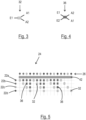
- the light sources 22 emit transmitted light 12 at the exit points to a photonic network 24. From the photonic network 24, the transmitted light 12 is selectively fed to various emission points 26. From the emission points 26, the transmitted light 12 enters the field of view 14 through a transmission optics designed as a lens 28. From each emission point 26, only a partial field of view 30 can be irradiated with transmitted light 12 and thus optically scanned.
Landscapes
- Physics & Mathematics (AREA)
- Engineering & Computer Science (AREA)
- General Physics & Mathematics (AREA)
- Computer Networks & Wireless Communication (AREA)
- Radar, Positioning & Navigation (AREA)
- Remote Sensing (AREA)
- Electromagnetism (AREA)
- Optics & Photonics (AREA)
- Optical Radar Systems And Details Thereof (AREA)
Claims (13)
- Capteur optoélectronique (10) pour détecter un objet (16) dans une zone de vision (14) du capteur (10), comprenant- plusieurs sources de lumière (22) pour produire une lumière d'émission (12), les sources de lumière (22) comprenant au moins une première et une deuxième source de lumière (22a, 22b),- une optique d'émission (28) pour projeter la lumière d'émission (12) dans la zone de vision (14),- au moins un détecteur pour détecter la lumière d'émission (18) renvoyée par l'objet (16),dans lequelles sources de lumière (22) émettent une lumière d'émission (12) vers un réseau photonique (24),le réseau photonique (24) présente plusieurs points de rayonnement (26) auxquels peut être amenée une lumière d'émission (12) respective de précisément une source de lumière (22) respective, plusieurs points de rayonnement (26) juxtaposés ou adjacents directement les uns aux autres étant conçus pour rayonner la lumière d'émission (12) dans plusieurs zones de vision partielles (30) juxtaposées ou adjacentes de préférence directement les unes aux autres,le réseau photonique (24) est conçu pour amener la lumière d'émission (12) de la même source de lumière (22) vers au moins deux points de rayonnement (26) différents,entre les deux points de rayonnement (26) différents, auxquels peut être amenée la lumière d'émission (12) de la première source de lumière (22a), est prévu au moins un point de rayonnement (26) auquel peut être amenée la lumière d'émission (12) de la deuxième source de lumière (22b), chaque source de lumière (22) fait partie d'un système FMCW respectif à canal unique pour mesurer la distance à l'objet (16),au moins les première et deuxième sources de lumière (22a, 22b) utilisent des longueurs d'onde et/ou des plages de longueurs d'onde différentes pour la lumière d'émission (12).
- Capteur optoélectronique (10) selon la revendication 1,
dans lequel le réseau photonique (24) comprend au moins un commutateur optique (32) pour chaque source de lumière (22), le commutateur respectif (32) étant conçu pour acheminer la lumière d'émission (12) vers au moins deux trajets lumineux différents dans le réseau photonique (24), afin d'amener la lumière d'émission (12) vers au moins deux points de rayonnement (26) différents. - Capteur optoélectronique (10) selon la revendication 1 ou 2,
dans lequel le réseau photonique (24) comprend au moins un croisement de guides d'ondes (36) pour amener la lumière d'émission (12) de la deuxième source de lumière (22b) vers le point de rayonnement (26) situé entre les deux points de rayonnement (26) différents auxquels peut être amenée la lumière d'émission (12) de la première source de lumière (22a). - Capteur optoélectronique (10) selon l'une des revendications précédentes, dans lequel le capteur (10) comprend au moins trois, quatre ou plus de quatre sources de lumière (22),
entre deux points de rayonnement (26) différents, auxquels peut être amenée la lumière d'émission (12) de la même source de lumière (22), est prévu un point de rayonnement (26) pour chaque autre source de lumière respective (22), auquel peut être amenée la lumière d'émission (12) de l'une des autres sources de lumière (22). - Capteur optoélectronique (10) selon l'une des revendications précédentes, dans lequel le réseau photonique (24) comprend un circuit photonique intégré comprenant en particulier le commutateur optique (32) et le croisement de guides d'ondes (36).
- Capteur optoélectronique (10) selon l'une des revendications précédentes, dans lequel les points de rayonnement (26) sont prévus le long d'une ligne droite, et/oule capteur optoélectronique (10) présente un groupe (40) de points de rayonnement (26) juxtaposés directement les uns aux autres, le nombre de points de rayonnement (26) dans le groupe (40) correspondant au nombre de sources de lumière (22), une lumière d'émission (12) d'une autre source de lumière (22) pouvant être amenée vers chacun des points de rayonnement (26) dans le groupe (40),plusieurs groupes (40) sont de préférence disposés les uns à la suite des autres.
- Capteur optoélectronique (10) selon l'une des revendications précédentes, dans lequel une partie des points de rayonnement (26) est conçue pour rayonner la lumière d'émission (12) dans des zones de vision partielles (30) disposées plus près les unes des autres.
- Capteur optoélectronique (10) selon l'une des revendications précédentes, dans lequel le capteur optoélectronique (10) est conçu pour amener la lumière d'émission (12) vers une partie des points de rayonnement (26) pendant une durée plus longue que vers les autres points de rayonnement (26) auxquels est amenée la lumière d'émission.
- Capteur optoélectronique (10) selon l'une des revendications précédentes, dans lequel le réseau photonique (24) comprend un premier étage (34) comprenant des commutateurs optiques (32) et des croisements de guides d'ondes (36), les commutateurs optiques (32) présentant chacun une entrée et deux sorties, les sorties de chaque commutateur (32) étant reliées à une pluralité de croisements de guides d'ondes (36), de sorte que les sorties d'un commutateur (32) croisent une fois au moins une sortie de chaque autre commutateur (32).
- Capteur optoélectronique (10) selon la revendication 9,
dans lequel le réseau photonique (24) comprend un deuxième et/ou un ou plusieurs autres étages (38) comprenant des commutateurs optiques (32) et des croisements de guides d'ondes (36), les commutateurs optiques (32) présentant chacun une entrée et deux sorties, les sorties de chaque commutateur (32) étant connectées à plusieurs croisements de guides d'ondes (36), de sorte que les sorties d'un commutateur (32) croisent une fois au moins une sortie de chaque autre commutateur (32), un commutateur optique (32) respectif du deuxième et/ou autre étage (38) étant prévu pour une sortie de l'étage précédent (34). - Capteur optoélectronique (10) selon l'une des revendications précédentes, dans lequel la lumière d'émission (18) renvoyée par l'objet (16) est injectée dans le réseau photonique (24) au niveau des points de rayonnement (26) et est amenée vers le détecteur au moyen du réseau photonique (24), de préférence, un détecteur séparé étant prévu pour chaque source de lumière (22).
- Procédé de fonctionnement d'un capteur optoélectronique (10), qui sert à détecter un objet (16) dans une zone de vision (14) du capteur (10), dans lequel- une première et une deuxième source de lumière (22a, 22b) produisent une lumière d'émission (12), les sources de lumière (22) émettant la lumière d'émission (12) vers un réseau photonique (24), la lumière d'émission (12) étant amenée à plusieurs points de rayonnement (26) du réseau photonique (24), la lumière d'émission (12) respective de précisément une source de lumière (22) respective étant amenée vers les points de rayonnement (26), la lumière d'émission (12) étant rayonnée à partir de plusieurs points de rayonnement (26) directement adjacents dans plusieurs zones de vision partielles (30) directement juxtaposées,- au moins un détecteur détecte la lumière d'émission (18) renvoyée par l'objet (16),la lumière d'émission (12) de la deuxième source de lumière (22b) est amenée vers au moins un point de rayonnement (26) qui se situe entre deux points de rayonnement (26) auxquels peut être amenée la lumière d'émission (12) de la première source de lumière (22a),chaque source de lumière (22) fait partie d'un système FMCW respectif à canal unique pour mesurer la distance à l'objet (16),au moins les première et deuxième sources de lumière (22a, 22b) utilisent des longueurs d'onde et/ou des plages de longueurs d'onde différentes pour la lumière d'émission (12).
- Procédé selon la revendication 12, dans lequel
le capteur optoélectronique (10) comprend au moins encore une troisième source de lumière (22), la lumière d'émission (12) de la première, de la deuxième et de la troisième source de lumière (22) étant amenée, en particulier simultanément, vers trois points de rayonnement (26) directement juxtaposés et étant rayonnée dans trois zones de vision partielles (30) directement juxtaposées.
Priority Applications (2)
| Application Number | Priority Date | Filing Date | Title |
|---|---|---|---|
| EP22157102.9A EP4231045B1 (fr) | 2022-02-16 | 2022-02-16 | Capteur optoélectronique |
| US18/110,020 US12607721B2 (en) | 2022-02-16 | 2023-02-15 | Optoelectronic sensor |
Applications Claiming Priority (1)
| Application Number | Priority Date | Filing Date | Title |
|---|---|---|---|
| EP22157102.9A EP4231045B1 (fr) | 2022-02-16 | 2022-02-16 | Capteur optoélectronique |
Publications (3)
| Publication Number | Publication Date |
|---|---|
| EP4231045A1 EP4231045A1 (fr) | 2023-08-23 |
| EP4231045B1 true EP4231045B1 (fr) | 2025-04-02 |
| EP4231045C0 EP4231045C0 (fr) | 2025-04-02 |
Family
ID=80682446
Family Applications (1)
| Application Number | Title | Priority Date | Filing Date |
|---|---|---|---|
| EP22157102.9A Active EP4231045B1 (fr) | 2022-02-16 | 2022-02-16 | Capteur optoélectronique |
Country Status (2)
| Country | Link |
|---|---|
| US (1) | US12607721B2 (fr) |
| EP (1) | EP4231045B1 (fr) |
Citations (1)
| Publication number | Priority date | Publication date | Assignee | Title |
|---|---|---|---|---|
| EP3916424A1 (fr) * | 2020-05-25 | 2021-12-01 | Scantinel Photonics GmbH | Dispositif et procédé de mesure par balayage de la distance à un objet |
Family Cites Families (12)
| Publication number | Priority date | Publication date | Assignee | Title |
|---|---|---|---|---|
| GB0625442D0 (en) * | 2006-12-20 | 2007-01-31 | Csl Surveys Stevenage Ltd | Profiling device |
| US10338321B2 (en) * | 2017-03-20 | 2019-07-02 | Analog Photonics LLC | Large scale steerable coherent optical switched arrays |
| US10254388B2 (en) | 2017-03-28 | 2019-04-09 | Luminar Technologies, Inc. | Dynamically varying laser output in a vehicle in view of weather conditions |
| US20180284234A1 (en) | 2017-03-29 | 2018-10-04 | Luminar Technologies, Inc. | Foveated Imaging in a Lidar System |
| DE102017107903A1 (de) * | 2017-04-12 | 2018-10-18 | Sick Ag | 3D-Lichtlaufzeitkamera und Verfahren zur Erfassung dreidimensionaler Bilddaten |
| US10641900B2 (en) | 2017-09-15 | 2020-05-05 | Aeye, Inc. | Low latency intra-frame motion estimation based on clusters of ladar pulses |
| US10613276B2 (en) * | 2018-06-08 | 2020-04-07 | Huawei Technologies Co., Ltd. | Optical scanner with optically switched paths to multiple surface or edge couplers |
| CN109633611B (zh) * | 2018-12-06 | 2020-02-07 | 上海交通大学 | 基于巴特勒矩阵的集成二维多波束激光雷达发射系统 |
| WO2021067911A1 (fr) * | 2019-10-04 | 2021-04-08 | University Of Rochester | Structure de réseau optique phasé et techniques de fabrication |
| DE102019133096A1 (de) | 2019-12-05 | 2021-06-10 | Sick Ag | Optoelektronischer Sensor und Verfahren zur Erfassung eines Objekts |
| US11378689B2 (en) | 2020-02-18 | 2022-07-05 | Analog Devices, Inc. | Highly multiplexed coherent LIDAR system |
| DE102020110142A1 (de) | 2020-04-14 | 2021-10-14 | Scantinel Photonics GmbH | Vorrichtung und Verfahren zur scannenden Messung des Abstands zu einem Objekt |
-
2022
- 2022-02-16 EP EP22157102.9A patent/EP4231045B1/fr active Active
-
2023
- 2023-02-15 US US18/110,020 patent/US12607721B2/en active Active
Patent Citations (1)
| Publication number | Priority date | Publication date | Assignee | Title |
|---|---|---|---|---|
| EP3916424A1 (fr) * | 2020-05-25 | 2021-12-01 | Scantinel Photonics GmbH | Dispositif et procédé de mesure par balayage de la distance à un objet |
Also Published As
| Publication number | Publication date |
|---|---|
| US12607721B2 (en) | 2026-04-21 |
| EP4231045A1 (fr) | 2023-08-23 |
| US20230258775A1 (en) | 2023-08-17 |
| EP4231045C0 (fr) | 2025-04-02 |
Similar Documents
| Publication | Publication Date | Title |
|---|---|---|
| EP0898783B1 (fr) | Microscope a balayage dans lequel un echantillon est excite optiquement simultanement en plusieurs points | |
| EP3916424A1 (fr) | Dispositif et procédé de mesure par balayage de la distance à un objet | |
| EP2917776B1 (fr) | Microscope optique et procédé de microscopie | |
| DE10225838B4 (de) | Verfahren zur Scanmikroskopie, Scanmikroskop und Vorrichtung zum Codieren eines Beleuchtungslichtstrahles | |
| DE102020110142A1 (de) | Vorrichtung und Verfahren zur scannenden Messung des Abstands zu einem Objekt | |
| DE2802417C2 (fr) | ||
| EP4162289B1 (fr) | Système lidar à commande grossière d'angle | |
| EP3832344B1 (fr) | Capteur optoélectronique et procédé de détection d'un objet | |
| EP2326915B1 (fr) | Procédé et dispositif de détection de données de contour et/ou de propriétés optiques d'un objet semi-transparent tridimensionnel | |
| DE102004037137A1 (de) | Verfahren und Vorrichtung zur Entfernungsmessung | |
| DE3905730C2 (de) | Positionsmeßeinrichtung | |
| DE112015001154T5 (de) | Mikroskop und Mikroskopie-Verfahren | |
| DE102017205889A1 (de) | Optische Anordnung zur Laserinterferenzstrukturierung einer Probe | |
| DE112020000407T5 (de) | Lidar-systeme und -verfahren mit strahllenkung und weitwinkelsignaldetektion | |
| DE102019125684A1 (de) | Optoelektronischer Sensor und Verfahren zur Erfassung von Objekten | |
| DE102021111949A1 (de) | Vorrichtung zur scannenden Messung des Abstands zu einem Objekt | |
| EP4231045B1 (fr) | Capteur optoélectronique | |
| EP2884241B1 (fr) | Système de détection de position et procédé de fonctionnement d'un système de détection de position | |
| DE202022100888U1 (de) | Optoelektronischer Sensor | |
| DE102016113909A1 (de) | Optische Sendeeinheit für eine optische Detektionsvorrichtung und Verfahren zum Betrieb einer optischen Sendeeinheit | |
| EP3631495A1 (fr) | Unite d'émission de rayonnement dans l'environnement | |
| EP2928280B1 (fr) | Système de repère pour l'étalonnage d'une machine | |
| EP3916423A1 (fr) | Dispositif et procédé de mesure par balayage de la distance à un objet | |
| EP4286886B1 (fr) | Capteur optoélectronique destiné à la mesure de distance doté d'une couche de routage | |
| DE102018117792A1 (de) | Vorrichtung zur ortsaufgelösten Abstands- und/oder Geschwindigkeitsermittlung eines Objekts |
Legal Events
| Date | Code | Title | Description |
|---|---|---|---|
| PUAI | Public reference made under article 153(3) epc to a published international application that has entered the european phase |
Free format text: ORIGINAL CODE: 0009012 |
|
| STAA | Information on the status of an ep patent application or granted ep patent |
Free format text: STATUS: EXAMINATION IS IN PROGRESS |
|
| 17P | Request for examination filed |
Effective date: 20230331 |
|
| AK | Designated contracting states |
Kind code of ref document: A1 Designated state(s): AL AT BE BG CH CY CZ DE DK EE ES FI FR GB GR HR HU IE IS IT LI LT LU LV MC MK MT NL NO PL PT RO RS SE SI SK SM TR |
|
| GRAP | Despatch of communication of intention to grant a patent |
Free format text: ORIGINAL CODE: EPIDOSNIGR1 |
|
| STAA | Information on the status of an ep patent application or granted ep patent |
Free format text: STATUS: GRANT OF PATENT IS INTENDED |
|
| INTG | Intention to grant announced |
Effective date: 20241010 |
|
| GRAS | Grant fee paid |
Free format text: ORIGINAL CODE: EPIDOSNIGR3 |
|
| GRAA | (expected) grant |
Free format text: ORIGINAL CODE: 0009210 |
|
| STAA | Information on the status of an ep patent application or granted ep patent |
Free format text: STATUS: THE PATENT HAS BEEN GRANTED |
|
| AK | Designated contracting states |
Kind code of ref document: B1 Designated state(s): AL AT BE BG CH CY CZ DE DK EE ES FI FR GB GR HR HU IE IS IT LI LT LU LV MC MK MT NL NO PL PT RO RS SE SI SK SM TR |
|
| REG | Reference to a national code |
Ref country code: GB Ref legal event code: FG4D Free format text: NOT ENGLISH |
|
| REG | Reference to a national code |
Ref country code: CH Ref legal event code: EP |
|
| REG | Reference to a national code |
Ref country code: IE Ref legal event code: FG4D Free format text: LANGUAGE OF EP DOCUMENT: GERMAN |
|
| U01 | Request for unitary effect filed |
Effective date: 20250402 |
|
| U07 | Unitary effect registered |
Designated state(s): AT BE BG DE DK EE FI FR IT LT LU LV MT NL PT RO SE SI Effective date: 20250408 |
|
| PG25 | Lapsed in a contracting state [announced via postgrant information from national office to epo] |
Ref country code: ES Free format text: LAPSE BECAUSE OF FAILURE TO SUBMIT A TRANSLATION OF THE DESCRIPTION OR TO PAY THE FEE WITHIN THE PRESCRIBED TIME-LIMIT Effective date: 20250402 |
|
| PG25 | Lapsed in a contracting state [announced via postgrant information from national office to epo] |
Ref country code: GR Free format text: LAPSE BECAUSE OF FAILURE TO SUBMIT A TRANSLATION OF THE DESCRIPTION OR TO PAY THE FEE WITHIN THE PRESCRIBED TIME-LIMIT Effective date: 20250703 Ref country code: NO Free format text: LAPSE BECAUSE OF FAILURE TO SUBMIT A TRANSLATION OF THE DESCRIPTION OR TO PAY THE FEE WITHIN THE PRESCRIBED TIME-LIMIT Effective date: 20250702 |
|
| PG25 | Lapsed in a contracting state [announced via postgrant information from national office to epo] |
Ref country code: PL Free format text: LAPSE BECAUSE OF FAILURE TO SUBMIT A TRANSLATION OF THE DESCRIPTION OR TO PAY THE FEE WITHIN THE PRESCRIBED TIME-LIMIT Effective date: 20250402 |
|
| PG25 | Lapsed in a contracting state [announced via postgrant information from national office to epo] |
Ref country code: HR Free format text: LAPSE BECAUSE OF FAILURE TO SUBMIT A TRANSLATION OF THE DESCRIPTION OR TO PAY THE FEE WITHIN THE PRESCRIBED TIME-LIMIT Effective date: 20250402 |
|
| PG25 | Lapsed in a contracting state [announced via postgrant information from national office to epo] |
Ref country code: RS Free format text: LAPSE BECAUSE OF FAILURE TO SUBMIT A TRANSLATION OF THE DESCRIPTION OR TO PAY THE FEE WITHIN THE PRESCRIBED TIME-LIMIT Effective date: 20250702 |
|
| PG25 | Lapsed in a contracting state [announced via postgrant information from national office to epo] |
Ref country code: IS Free format text: LAPSE BECAUSE OF FAILURE TO SUBMIT A TRANSLATION OF THE DESCRIPTION OR TO PAY THE FEE WITHIN THE PRESCRIBED TIME-LIMIT Effective date: 20250802 |
|
| PG25 | Lapsed in a contracting state [announced via postgrant information from national office to epo] |
Ref country code: SM Free format text: LAPSE BECAUSE OF FAILURE TO SUBMIT A TRANSLATION OF THE DESCRIPTION OR TO PAY THE FEE WITHIN THE PRESCRIBED TIME-LIMIT Effective date: 20250402 |
|
| PG25 | Lapsed in a contracting state [announced via postgrant information from national office to epo] |
Ref country code: CZ Free format text: LAPSE BECAUSE OF FAILURE TO SUBMIT A TRANSLATION OF THE DESCRIPTION OR TO PAY THE FEE WITHIN THE PRESCRIBED TIME-LIMIT Effective date: 20250402 |
|
| PG25 | Lapsed in a contracting state [announced via postgrant information from national office to epo] |
Ref country code: SK Free format text: LAPSE BECAUSE OF FAILURE TO SUBMIT A TRANSLATION OF THE DESCRIPTION OR TO PAY THE FEE WITHIN THE PRESCRIBED TIME-LIMIT Effective date: 20250402 |
|
| PLBE | No opposition filed within time limit |
Free format text: ORIGINAL CODE: 0009261 |
|
| STAA | Information on the status of an ep patent application or granted ep patent |
Free format text: STATUS: NO OPPOSITION FILED WITHIN TIME LIMIT |
|
| REG | Reference to a national code |
Ref country code: CH Ref legal event code: L10 Free format text: ST27 STATUS EVENT CODE: U-0-0-L10-L00 (AS PROVIDED BY THE NATIONAL OFFICE) Effective date: 20260211 |
|
| 26N | No opposition filed |
Effective date: 20260105 |
|
| U20 | Renewal fee for the european patent with unitary effect paid |
Year of fee payment: 5 Effective date: 20260224 |