EP4231666A1 - Mems-vorrichtung - Google Patents
Mems-vorrichtung Download PDFInfo
- Publication number
- EP4231666A1 EP4231666A1 EP22157127.6A EP22157127A EP4231666A1 EP 4231666 A1 EP4231666 A1 EP 4231666A1 EP 22157127 A EP22157127 A EP 22157127A EP 4231666 A1 EP4231666 A1 EP 4231666A1
- Authority
- EP
- European Patent Office
- Prior art keywords
- piezoelectric
- transducer
- piezoelectric transducer
- mems device
- bias
- Prior art date
- Legal status (The legal status is an assumption and is not a legal conclusion. Google has not performed a legal analysis and makes no representation as to the accuracy of the status listed.)
- Pending
Links
Images


Classifications
-
- H—ELECTRICITY
- H04—ELECTRIC COMMUNICATION TECHNIQUE
- H04R—LOUDSPEAKERS, MICROPHONES, GRAMOPHONE PICK-UPS OR LIKE ACOUSTIC ELECTROMECHANICAL TRANSDUCERS; ELECTRIC HEARING AIDS; PUBLIC ADDRESS SYSTEMS
- H04R17/00—Piezoelectric transducers; Electrostrictive transducers
- H04R17/02—Microphones
-
- H—ELECTRICITY
- H04—ELECTRIC COMMUNICATION TECHNIQUE
- H04R—LOUDSPEAKERS, MICROPHONES, GRAMOPHONE PICK-UPS OR LIKE ACOUSTIC ELECTROMECHANICAL TRANSDUCERS; ELECTRIC HEARING AIDS; PUBLIC ADDRESS SYSTEMS
- H04R17/00—Piezoelectric transducers; Electrostrictive transducers
- H04R17/10—Resonant transducers, i.e. adapted to produce maximum output at a predetermined frequency
-
- H—ELECTRICITY
- H04—ELECTRIC COMMUNICATION TECHNIQUE
- H04R—LOUDSPEAKERS, MICROPHONES, GRAMOPHONE PICK-UPS OR LIKE ACOUSTIC ELECTROMECHANICAL TRANSDUCERS; ELECTRIC HEARING AIDS; PUBLIC ADDRESS SYSTEMS
- H04R1/00—Details of transducers, loudspeakers or microphones
- H04R1/02—Casings; Cabinets ; Supports therefor; Mountings therein
- H04R1/04—Structural association of microphone with electric circuitry therefor
-
- B—PERFORMING OPERATIONS; TRANSPORTING
- B81—MICROSTRUCTURAL TECHNOLOGY
- B81B—MICROSTRUCTURAL DEVICES OR SYSTEMS, e.g. MICROMECHANICAL DEVICES
- B81B7/00—Microstructural systems; Auxiliary parts of microstructural devices or systems
- B81B7/008—MEMS characterised by an electronic circuit specially adapted for controlling or driving the same
-
- H—ELECTRICITY
- H04—ELECTRIC COMMUNICATION TECHNIQUE
- H04R—LOUDSPEAKERS, MICROPHONES, GRAMOPHONE PICK-UPS OR LIKE ACOUSTIC ELECTROMECHANICAL TRANSDUCERS; ELECTRIC HEARING AIDS; PUBLIC ADDRESS SYSTEMS
- H04R19/00—Electrostatic transducers
- H04R19/005—Electrostatic transducers using semiconductor materials
-
- H—ELECTRICITY
- H04—ELECTRIC COMMUNICATION TECHNIQUE
- H04R—LOUDSPEAKERS, MICROPHONES, GRAMOPHONE PICK-UPS OR LIKE ACOUSTIC ELECTROMECHANICAL TRANSDUCERS; ELECTRIC HEARING AIDS; PUBLIC ADDRESS SYSTEMS
- H04R3/00—Circuits for transducers
-
- H—ELECTRICITY
- H04—ELECTRIC COMMUNICATION TECHNIQUE
- H04R—LOUDSPEAKERS, MICROPHONES, GRAMOPHONE PICK-UPS OR LIKE ACOUSTIC ELECTROMECHANICAL TRANSDUCERS; ELECTRIC HEARING AIDS; PUBLIC ADDRESS SYSTEMS
- H04R3/00—Circuits for transducers
- H04R3/04—Circuits for transducers for correcting frequency response
- H04R3/06—Circuits for transducers for correcting frequency response of electrostatic transducers
-
- H—ELECTRICITY
- H04—ELECTRIC COMMUNICATION TECHNIQUE
- H04R—LOUDSPEAKERS, MICROPHONES, GRAMOPHONE PICK-UPS OR LIKE ACOUSTIC ELECTROMECHANICAL TRANSDUCERS; ELECTRIC HEARING AIDS; PUBLIC ADDRESS SYSTEMS
- H04R7/00—Diaphragms for electromechanical transducers; Cones
- H04R7/02—Diaphragms for electromechanical transducers; Cones characterised by the construction
- H04R7/04—Plane diaphragms
- H04R7/06—Plane diaphragms comprising a plurality of sections or layers
-
- B—PERFORMING OPERATIONS; TRANSPORTING
- B81—MICROSTRUCTURAL TECHNOLOGY
- B81B—MICROSTRUCTURAL DEVICES OR SYSTEMS, e.g. MICROMECHANICAL DEVICES
- B81B2201/00—Specific applications of microelectromechanical systems
- B81B2201/02—Sensors
- B81B2201/0257—Microphones or microspeakers
-
- B—PERFORMING OPERATIONS; TRANSPORTING
- B81—MICROSTRUCTURAL TECHNOLOGY
- B81B—MICROSTRUCTURAL DEVICES OR SYSTEMS, e.g. MICROMECHANICAL DEVICES
- B81B2203/00—Basic microelectromechanical structures
- B81B2203/01—Suspended structures, i.e. structures allowing a movement
- B81B2203/0127—Diaphragms, i.e. structures separating two media that can control the passage from one medium to another; Membranes, i.e. diaphragms with filtering function
-
- B—PERFORMING OPERATIONS; TRANSPORTING
- B81—MICROSTRUCTURAL TECHNOLOGY
- B81B—MICROSTRUCTURAL DEVICES OR SYSTEMS, e.g. MICROMECHANICAL DEVICES
- B81B2207/00—Microstructural systems or auxiliary parts thereof
- B81B2207/03—Electronic circuits for micromechanical devices which are not application specific, e.g. for controlling, power supplying, testing, protecting
-
- H—ELECTRICITY
- H04—ELECTRIC COMMUNICATION TECHNIQUE
- H04R—LOUDSPEAKERS, MICROPHONES, GRAMOPHONE PICK-UPS OR LIKE ACOUSTIC ELECTROMECHANICAL TRANSDUCERS; ELECTRIC HEARING AIDS; PUBLIC ADDRESS SYSTEMS
- H04R1/00—Details of transducers, loudspeakers or microphones
- H04R1/20—Arrangements for obtaining desired frequency or directional characteristics
- H04R1/22—Arrangements for obtaining desired frequency or directional characteristics for obtaining desired frequency characteristic only
- H04R1/28—Transducer mountings or enclosures modified by provision of mechanical or acoustic impedances, e.g. resonator, damping means
-
- H—ELECTRICITY
- H04—ELECTRIC COMMUNICATION TECHNIQUE
- H04R—LOUDSPEAKERS, MICROPHONES, GRAMOPHONE PICK-UPS OR LIKE ACOUSTIC ELECTROMECHANICAL TRANSDUCERS; ELECTRIC HEARING AIDS; PUBLIC ADDRESS SYSTEMS
- H04R19/00—Electrostatic transducers
- H04R19/04—Microphones
-
- H—ELECTRICITY
- H04—ELECTRIC COMMUNICATION TECHNIQUE
- H04R—LOUDSPEAKERS, MICROPHONES, GRAMOPHONE PICK-UPS OR LIKE ACOUSTIC ELECTROMECHANICAL TRANSDUCERS; ELECTRIC HEARING AIDS; PUBLIC ADDRESS SYSTEMS
- H04R2201/00—Details of transducers, loudspeakers or microphones covered by H04R1/00 but not provided for in any of its subgroups
- H04R2201/003—Mems transducers or their use
Definitions
- Piezoelectric MEMS devices may be implemented as MEMS sound transducers in form of MEMS microphones or MEMS loudspeakers, for example.
- MEMS microphones are used for recording ambient sound or ambient noise.
- MEMS loudspeakers are used for emitting acoustic or ultrasonic sound to the environment.
- MEMS sound transducers have a frequently still considerable variation in the frequency response, for example owing to process variations during manufacture or to package variations or, potentially, to ambient influences during operation of the sound transducer.
- the frequency response e.g. the sensitivity, the low-frequency roll-off (LFRO) and/or the resonance of a piezoelectric MEMS device
- LFRO low-frequency roll-off
- the resonance of a piezoelectric MEMS device can vary considerably.
- a tight trimming of the sensor sensitivity and frequency response is often mandatory for the products.
- a structure pre-bending due to material pre-stress can lead to an uncontrolled and inconsistent LFRO among piezoelectric MEMS devices of the same type.
- Fig. 9 shows a graph depicting the sensitivity of different MEMS devices (samples 1 - 5) as a function of the frequency of the output/input signal of the piezoelectric MEMS device.
- An ASIC Application Specific Integrated Circuit
- ASIC Application Specific Integrated Circuit
- PGA programmable gain amplifier
- SNR signal-to-noise ratio
- trimming the sensitivity to the desired target value fails to help to control the resonance behavior, e.g. the resonance frequencies, or the LFRO of the piezoelectric MEMS device.
- a MEMS device comprises a piezoelectric transducer (actuator or sensor) having a first frequency behavior, wherein the piezoelectric transducer comprises a piezoelectric trimming region, and a control circuitry configured to provide a bias signal to the piezoelectric trimming region of the piezoelectric transducer for adjusting a second frequency behavior (a target behavior) of the piezoelectric transducer.
- the piezoelectric transducer comprises a (first) piezoelectric transducing element (e.g. a piezoelectric layer), wherein at least a part of the (first) piezoelectric transducing element forms the piezoelectric trimming region.
- a (first) piezoelectric transducing element e.g. a piezoelectric layer
- the piezoelectric transducer comprises a (first) piezoelectric transducing element (e.g. a piezoelectric layer) and a further (second) piezoelectric transducing element, wherein the further (second) piezoelectric transducing element forms the piezoelectric trimming region.
- first piezoelectric transducing element e.g. a piezoelectric layer
- second piezoelectric transducing element forms the piezoelectric trimming region.
- the (first) piezoelectric transducing element and the further (second) piezoelectric transducing element may be formed as separate piezoelectric transducing elements.
- the term "separate" piezoelectric transducing elements relates to the embodiments which describe an "additional" trimming electrode, i.e. the further (second) piezoelectric transducing element (e.g. as an external trimming ring or an internal trimming electrode).
- exemplary embodiments of the present disclosure provide different approaches to trim the frequency response of piezoelectric MEMS devices.
- the frequency response e.g. in form of the sensitivity, the LFRO, the resonance frequency (resonance behavior), the total harmonic distortion (THD) and/or the acoustic overload point (AOP) of the MEMS device having a piezoelectric transducer can be individually trimmed, e.g. during a final product test or even during the (ongoing) operation of the piezoelectric MEMS device, e.g. in response to instantaneous environmental conditions.
- piezoelectric MEMS devices can be individually trimmed to meet a tight target specification.
- a bias signal (e.g. a bias voltage) is used, for example in addition to the PGA, to trim the frequency behavior of the piezoelectric transducer of the MEMS device without impacting the resulting SNR.
- a main surface region e.g. a displaceable or deflectable membrane
- a reference plane x-y-plane
- lateral means a direction parallel to the x- and/or y-direction or a direction parallel to (or in) the x-y-plane, wherein the term “vertical” means a direction parallel to the z-direction.
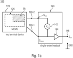
- Figs. 1a-b show an exemplary schematic illustration of the MEMS device 100 having a piezoelectric transducer 120, e.g. a two terminal piezoelectric device, and a control circuitry 140 (with a biasing and read-out function) according to an embodiment.
- the MEMS device 100 comprises the piezoelectric transducer 120, e.g. in form of an actuator (e.g. a loudspeaker) or a sensor (e.g. a microphone), having a first frequency behavior, wherein the piezoelectric transducer 120 comprises a piezoelectric trimming region TR.
- the MEMS device 100 comprises a control circuitry 140 configured to provide a bias signal S BIAS , e.g. a bias voltage V DC , to the piezoelectric trimming region TR of the piezoelectric transducer 120 for adjusting a second frequency behavior (target behavior) of the piezoelectric transducer 120.
- a bias signal S BIAS e.g. a bias voltage V DC
- the piezoelectric transducer 120 comprises a (first) piezoelectric transducing element 126, e.g. in form of a piezoelectric layer or structure, wherein at least a part of the (first) piezoelectric transducing element 126 or the complete (first) piezoelectric transducing element 126 forms the piezoelectric trimming region TR.
- the piezoelectric transducer 120 may be implemented as a two terminal piezoelectric device having a first terminal (contact or pad) 128-1, e.g. a sense or control terminal, and a second terminal (contact or pad) 128-2, e.g. a bias terminal.
- the first terminal 128-1 forms a sense terminal for outputting the sense signal S SENSE .
- the first terminal 128-1 forms a drive terminal for receiving a drive signal, for example (e.g. see also Fig. 3a-b and the associated description below).
- Fig. 1a shows a schematic equivalent circuit of the MEMS device 100 having the piezoelectric MEMS transducer 120 and the control circuitry 140
- Fig. 1b shows an exemplary technical implementation of the piezoelectric MEMS transducer 120
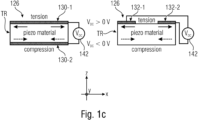
- the piezoelectric MEMS transducer 120 may have a membrane structure 122, the piezoelectric (layer) structure 126 and the contact structures (contact layers) 130, 132 which are connected to contact regions (or pads) 128-1, 128-2.
- the piezoelectric transducer 120 has a membrane structure 122, wherein the piezoelectric transducing element 126 is fixed (e.g.
- the membrane structure 122 may comprise (may be made) at least partially or completely (of) piezoelectric material.
- the membrane structure 122 may comprise a diaphragm (e.g. having a metallic, plastic, insulating or semiconductor material, e.g. poly-Si, etc.), wherein the piezoelectric transducing element 126 is fixed (e.g. mechanically coupled or attached) to the diaphragm.
- the piezoelectric transducing element 126 itself may form the membrane structure 122, wherein the membrane structure 122 may consist of or may comprise the piezoelectric material of the piezoelectric transducing element 126.
- the contact regions 128-1, 128-2 provide for electrical contacts and connections from the contact structures (contact layers) 130, 132 (see e.g. Fig. 1c ) of the piezoelectric (layer) structure 126 to the control circuitry 140 of the MEMS device 100.
- the control circuitry 140 is configured to read out the sense signal S SENSE from the piezoelectric MEMS transducer 120 at the first terminal 128-1 and to provide the bias signal S BIAS at the second terminal 128-2 to the piezoelectric MEMS transducer 120.
- the piezoelectric layer or structure 126 may partially or completely cover a main surface region (e.g. front or back side) of the membrane structure 122, wherein the electrodes (or terminals) 130, 132 cover partially or completely the piezoelectric layer or structure 126.
- the electrodes (or terminals) 130, 132 may cover (partially or completely) the (active) areas of the piezoelectric layer or structure 126.
- the piezoelectric MEMS transducer 120 may be segmented, i.e. may comprise a segmented membrane structure 122 having the membrane segments I, II, III, IV and a segmented piezoelectric (layer) structure 126 having accordingly formed piezoelectric structure segments and may comprise a segmented contact structure (contact layer) 130, 132 having accordingly formed contact structure (contact layer) segments, wherein the (e.g. four) segments I, II, III and IV of the piezoelectric MEMS transducer 120 are serially connected.
- the piezoelectric MEMS transducer 120 may also comprise a continuous (not-segmented or one-piece) structure.
- the piezoelectric transducer 120 may be implemented as a piezoelectric sensor.
- the piezoelectric sensor uses the piezoelectric effect to measure changes in pressure, acceleration, temperature, strain, or force by converting them to an electrical charge.
- the piezoelectric transducer 120 has (usually) a (very) high DC output impedance and can be modeled as a proportional voltage source.
- the output voltage S SENSE of the piezoelectric sensor 120 is directly proportional to the applied force, pressure, or strain, i.e. to the force, pressure, or strain applied to the displaceable or deflectable membrane structure 122 of the piezoelectric transducer 120
- the piezoelectric transducer 120 may be also implemented as an actuator, e.g. in form of a piezoelectric speaker (loudspeaker or piezo bender due to its mode of operation) that uses the piezoelectric effect for generating sound.
- the initial mechanical motion is created by applying a voltage to a piezoelectric material, and this motion is typically converted into audible sound or ultrasonic sound using a diaphragm (membrane).
- a diaphragm membrane
- Fig. 1c shows a schematic cross-sectional view of an exemplary piezoelectric structure 126 of the piezoelectric transducer 120 and exemplary biasing conditions of the piezoelectric structure 126 according to the embodiment.
- the piezoelectric transducer 120 of Figs. 1a-b is implemented as a piezoelectric sensor, which provides the sensor output signal S SENSE based on a deflection of the membrane structure 122 due to an acoustic or ultrasonic sound signal or a noise signal received from the environment of the MEMS device 100.
- Fig. 1c shows a schematic cross-sectional view of an exemplary trimming region TR of the piezoelectric structure 126 of the piezoelectric transducer 120 and exemplary biasing conditions of the trimming region TR according to the embodiment.
- different strain conditions exerted on the piezoelectric material of the piezoelectric trimming region TR of the piezoelectric transducer 126 which results in different biasing conditions of the piezoelectric trimming region TR of the piezoelectric transducer 126 of the MEMS device 100.
- the magnitude and extent of the strain conditions in the piezoelectric material of the piezoelectric trimming region TR of the piezoelectric transducer 126 can be adjusted.
- the contact structures 132-1, 132-2 may be arranged on the same surface region (e.g. the front or back side) of the piezoelectric layer TR in a laterally spaced and separated arrangement.
- the DC voltage V DC is applied to a specific physical region TR of a piezoelectric MEMS device 120 to trim its mechanical and system properties to a desired target specification.
- the control circuitry 140 is connected to the first and second terminal 128-1, 128-2 of the piezoelectric transducer 120, wherein the first terminal 128-1 forms a sense and/or control terminal, and the second terminal 128-2 forms a bias terminal of the piezoelectric transducer 120.
- the voltage source 142 is connected between the first and second terminal 128-1, 128-2 of the piezoelectric transducer 120.
- the bias signal S BIAS e.g. a DC bias voltage V DC
- the first terminal (output terminal) 128-1 of the piezoelectric transducer 120 is connected to a signal buffer 144 of the control circuitry 140 for providing the output signal S OUT of the MEMS device 100, e.g. in a single-ended readout configuration, to the output terminal 146.
- the signal level of the output signal S OUT at the output terminal 146 may be related to a reference potential (reference voltage) GND, e.g. ground potential.
- the sense (output) signal S SENSE of the piezoelectric transducer 120 is 'buffered from' the load (or currents produced by the load).
- the piezoelectric MEMS device 100 may be implemented as a piezoelectric MEMS sensor based on inverse piezoelectric effect, wherein the MEMS device 100 uses a bias voltage S BIAS which is applied between the electrodes 128-1, 128-2 of the piezoelectric MEMS transducer 120.
- the DC voltage applied to the MEMS transducer 120 causes a mechanical reaction in the MEMS transducer 120 (due to the direct piezoelectric effect).
- the generated strain/stress leads to a deformation or deflection of the MEMS structure 122, e.g. the membrane structure 122.
- Such a deformation can be used to trim the sensitivity, e.g. by counteracting the impact of material pre-stress hence making the whole structure softer/harder, and/or to trim the frequency response (LFRO and resonance).
- LFRO can be adjusted if the device deformation under bias leads to a physical change of the acoustic properties of the system, e.g. a variation of the size of the ventilation hole (see also for example Figs. 8a -c and the associated text passages of the description).
- exemplary embodiments of the present disclosure provide different trimming approaches suitable for piezoelectric MEMS devices during the frequency response of the piezoelectric MEMS device, such as the sensitivity, the LFRO, the resonance frequency (resonance behavior) ), the total harmonic distortion (THD) and/or the acoustic overload point (AOP) of the piezoelectric transducer 120 of the MEMS device having a piezoelectric transducer can be individually trimmed, e.g. during a final product test or even during the (ongoing) operation of the piezoelectric MEMS device.
- piezoelectric MEMS devices can be individually trimmed to meet a tight target specification.
- the described trimming and/or adjusting of the frequency behavior of the piezoelectric MEMS transducer 120 can be used for the initial microphone trimming but also during operation.
- the frequency response of the piezoelectric MEMS device e.g. the sensitivity, LFRO, resonance behavior, a total harmonic distortion (THD), or the acoustic overload point (AOP)
- TDD total harmonic distortion
- AOP acoustic overload point
- the trimming of the piezoelectric MEMS transducer 120 can be conducted to adapt the frequency response to the respective environmental conditions.
- Fig. 2 shows an schematic illustration of a change of a frequency behavior, i.e. a resonance shift, of the piezoelectric transducer 120 based on the applied bias signal S BIAS according to an embodiment.
- the resonance shift is measured by means of a impedance analyzer (LCR), for example.
- LCR impedance analyzer
- the degree or amount of the resonance shift depends on the design of the structure of the piezoelectric MEMS transducer 120.
- a continuous (not-segmented) piezoelectric MEMS transducer 120 (I) shows a larger dependency of the resonance shift from the bias signal S BIAS than a segmented piezoelectric MEMS transducer 120 (II) having e.g. six serially connected segments.
- the bias signal S BIAS is applied between the readout pins 128-1, 128-2 (first and second terminals).
- the bias voltage By applying the bias voltage between the readout pins 128, 122 of the piezoelectric MEMS transducer 120, the target frequency behavior of the piezoelectric MEMS transducer 120 can be adjusted.
- Fig. 2 show wafer level resonance shift measurements, wherein also the sensitivity (or the frequency response in general) can be adapted (e.g. an increased sensitivity can be achieved) by means of applying the bias voltage (having the right polarity) between the first and second terminals 128-1, 128-2 (pin 1, pin 2) of the piezoelectric MEMS transducer 120.
- Figs. 3a-c show different exemplary measured resonance shifts depending on the applied bias signal S BIAS in an actor operation of the piezoelectric transducer 120 according to an embodiment 120.
- the piezoelectric transducer 120 may be implemented as an actuator, e.g. in form of a piezoelectric speaker that uses the piezoelectric effect for generating sound, e.g. in the acoustic or ultrasonic frequency range.
- the bias signal S BIAS e.g. a bias voltage V DC
- V DC bias voltage
- the initial mechanical motion is created by applying with an AC signal source 143 an alternating signal (voltage) V AC to a piezoelectric transducing element 126, and this motion is typically converted into sound, e.g.
- Fig. 3c shows the resonance shift results performed with the LDV in a vacuum environment for the piezoelectric MEMS transducer 120.
- the sample chip having the MEMS transducer 120 is actuated with a DC bias voltage and an AC voltage whose frequency is swept from 1 kHz to 100 kHz.
- the actuation occurs between the readout electrodes 128-1, 128-2. Therefore, the sample is operated as an actor (micro-speaker), which emits acoustic waves at different frequencies.
- a maximal pressure is achieved at the first resonance frequency, hence at the peak of the frequency response.
- the peak position changes with the applied bias voltage S BIAS .
- the piezoelectric MEMS transducer 120 of the MEMS device 100 can be optimally operated at different working frequencies (operating frequencies) by changing the applied bias voltage.
- This trimming principle can also be used in ultrasonic applications with tunable working frequencies, e.g. for highly miniaturized distance measurement systems.
- the piezoelectric MEMS device 100 may be implemented as a piezoelectric MEMS actor based on the piezoelectric effect, wherein the MEMS device 100 uses a AC voltage V AC for operating and driving the piezoelectric MEMS transducer 120 and, also, uses a bias voltage S BIAS (V DC ) which is applied between the driving electrodes 128-1, 128-2 of the piezoelectric MEMS transducer 120 for adjusting the target behavior of the frequency response of the piezoelectric transducer 120.
- V DC bias voltage
- the DC voltage S BIAS applied to the MEMS transducer 120 causes a mechanical reaction in the MEMS transducer 120 (due to the direct piezoelectric effect).
- the generated strain/stress leads to a deformation or deflection of the MEMS structure 122, e.g. the membrane structure 120.
- a deformation can be used to trim the sensitivity, e.g. by counteracting the impact of material pre-stress hence making the whole structure softer/harder, and/or to trim the frequency response (e.g. LFRO and/or resonance) of the membrane structure 122.
- LFRO can be adjusted if the device deformation under bias leads to a physical change of the acoustic properties of the system, e.g. a variation of the size of ventilation holes (see also, for example, Figs. 6a-c and the associated text passages of the description).
- the same principle can be used to correct for manufacturing variations of the MEMS product in order to meet a defined target specification.
- the actuation voltage S DRIVE can be applied between each set of electrodes (readout, control, both) of the piezoelectric MEMS transducer 120.
- the MEMS device 100 comprises a piezoelectric transducer 120 (actuator or sensor) having a first frequency behavior, wherein the piezoelectric transducer 120 comprises a piezoelectric trimming region TR, and a control circuitry 140 configured to provide a bias signal S BIAS with respect to a first reference potential, e.g. ground GND1, to the piezoelectric trimming region 126 of the piezoelectric transducer 120 for adjusting a second frequency behavior (target behavior) of the piezoelectric transducer 120.
- a first reference potential e.g. ground GND1
- the piezoelectric transducer 120 comprises a (first) piezoelectric transducing element (piezoelectric layer) 126 and a further (second) piezoelectric transducing element TR, wherein the further (second) piezoelectric transducing 127 element forms the piezoelectric trimming region TR.
- the piezoelectric transducer 120 has a membrane structure 122, wherein the piezoelectric transducing element 126 and the further piezoelectric transducing element 127 are fixed to or form the membrane structure 122.
- the membrane structure 122 may comprise (may be made) at least partially or completely (of) piezoelectric material.
- the membrane structure 122 may comprise a diaphragm (e.g. having a metallic, plastic, insulating or semiconductor material, e.g. poly-Si, etc.), wherein the piezoelectric transducing element 126 and the further piezoelectric transducing element 127 may be fixed (e.g. mechanically coupled or attached) to the diaphragm.
- the piezoelectric transducing element 126 and the further piezoelectric transducing element 127 may form the membrane structure 122, wherein the membrane structure 122 may consist of or may comprise the piezoelectric material of the piezoelectric transducing element 126 and of the further piezoelectric transducing element 127.
- the (first) piezoelectric transducing element 126 and the further (second) piezoelectric transducing element 127 may be formed as separate piezoelectric transducing elements 126, 127.
- the term "separate" piezoelectric transducing elements 126, 127 relates to the embodiments which describe the further (second) piezoelectric transducing element 127, such as an "additional" trimming electrode, e.g. as an external trimming ring or an internal trimming electrode.
- the MEMS device 100 comprises the piezoelectric transducer 120 (e.g. a two terminal piezoelectric device with a control electrode) and a control circuitry 140 (with a biasing and readout function).
- Fig. 4a shows a schematic equivalent circuit of the MEMS device 100 having the piezoelectric MEMS transducer 120 and the control circuitry 140, wherein Fig. 4b shows an exemplary technical implementation of the piezoelectric MEMS transducer 120, and wherein Fig. 4c shows an enlarged cross-sectional partial view of the piezoelectric MEMS transducer 120.
- Fig. 4d shows an enlarged cross-sectional partial view of the trimming region TR of the piezoelectric MEMS transducer 120 along the section line A-A' in Fig. 4b .
- the terminal 128-2 forms a control electrode for the second piezoelectric (layer) structure 127 to provide a bias signal S BIAS with respect to a first reference potential, e.g. ground GND1, at the third terminal 128-3.
- the contact regions 128-1, 128-2, 128-3, 128-4 provide for electrical contacts and connections of the first and second piezoelectric structures 126, 127 to the control circuitry 140 of the MEMS device 100.
- the voltage source V DC 142 is connected between the second and third terminal 128-2, 128-3 of the piezoelectric transducer 120, i.e. the control bias S BIAS is applied between the control electrodes 128-2, 128-3, to provide the bias signal S BIAS with respect to a first reference potential, e.g. ground GND1, at the third terminal 128-3.
- the first terminal 128-1 forms the sense terminal for outputting the sense signal S SENSE with respect to a second reference potential, e.g. ground GND2, at the fourth terminal 128-4.
- the terminals 128-3, 128-4 may be formed as separate ground terminals 128-3, 128-4.
- a separated ground connection e.g. with different reference potentials GND1 and GND2 can be provided for the control electronics and the sense electronics.
- GND1 GND2
- GND1 GND2
- the second piezoelectric (layer) structure 127 is mechanically coupled (attached) to a further region or further regions of the membrane structure 122, e.g. to a border region 122-A and/or to a center region 122-B of the membrane structure 122.
- the second piezoelectric (layer) structure 127 may also comprise a plurality of partial structures 127 (I), 127 (II), which are arranged at different regions 122-A (border region), 122-B (center region) of the membrane structure 122 for trimming and/or adjusting of the frequency behavior of the piezoelectric MEMS transducer 120.
- a control electrode terminal 128-3 may be provided for each piezoelectric partial structure 127.
- the second piezoelectric (layer) structure 127 may also comprise only one piezoelectric structure 127, which is arranged at the membrane structure 122 for trimming and/or adjusting of the frequency behavior of the piezoelectric MEMS transducer 120.
- the second piezoelectric (layer) structure 127 may comprise an external trimming ring as the trimming region TR.
- the external trimming ring may be introduced as a ring electrode 127 at the outer rim 122-A of the membrane 122 to tune the resonance behavior, e.g. the resonance frequency, hence the sensitivity, by trimming the membrane compliance.
- Such a tuning principle recalls the tuning of a drum.
- an internal trimming electrode TR at the center region 122-B of the membrane 122 wherein the internal trimming electrode TR at the center region 122-B introduces strain/stress in the center part of the device 122.
- the bias signal application on the control electrode 128-2 can be performed using a specific ASIC output.
- the MEMS signal read-out and bias control can run on different channels, i.e. may be separated and independent.
- the piezoelectric MEMS transducer 120 may be segmented, i.e. may comprise a segmented membrane structure 122 and a segmented piezoelectric (layer) structure 126, wherein the (e.g. four or six) segments of the piezoelectric MEMS transducer 120 are serially connected.
- the piezoelectric MEMS transducer 120 may comprise a continuous (not-segmented or one-piece) structure.
- the second piezoelectric (layer) structure(s) 127 may (each) comprise a continuous (not-segmented or one-piece) structure.
- the piezoelectric transducer 120 may be implemented as a piezoelectric sensor for conducting a sensor operation.
- the piezoelectric sensor uses the piezoelectric effect to measure changes in pressure, acceleration, temperature, strain, or force by converting them to an electrical charge.
- the piezoelectric transducer 120 has (usually) a (very) high DC output impedance and can be modeled as a proportional voltage source.
- the output voltage S SENSE of the piezoelectric sensor 120 is directly proportional to the applied force, pressure, or strain, i.e. to the force, pressure, or strain applied to the displaceable or deflectable membrane structure 122 of the piezoelectric transducer 120
- the piezoelectric transducer 120 may be also implemented as an actuator, e.g. in form of a piezoelectric speaker (loudspeaker or piezo bender due to its mode of operation) that uses the piezoelectric effect for generating sound.
- the initial mechanical motion is created by applying a voltage to a piezoelectric material, and this motion is typically converted into audible sound using a diaphragm (membrane).
- a diaphragm membrane
- the control circuitry 140 is connected to the first, second and third terminal 128-1, 128-2, 128-3 of the piezoelectric transducer 120, wherein the first terminal 128-1 forms a sense terminal, the second terminal 128-2 forms a bias terminal, and the third terminal 128-3 forms a reference terminal (which is connected to a reference potential GND, e.g. ground potential) of the piezoelectric transducer 120.
- the voltage source V DC 142 is connected between the second and third terminal 128-2, 128-3 of the piezoelectric transducer 120.
- the first terminal (output terminal) 128-1 of the piezoelectric transducer 120 is connected to a signal buffer 144 of the control circuitry 140 for providing the output signal S OUT of the MEMS device 100 (e.g. in a single-ended readout configuration) to the output terminal 146.
- the signal level of the output signal S OUT at the output terminal 146 may be related to a reference potential GND, e.g. ground potential.
- the piezoelectric MEMS device 100 may be implemented as a piezoelectric MEMS sensor based on inverse piezoelectric effect, wherein the MEMS device 100 uses a bias voltage S BIAS which is applied between the electrodes 128-2, 128-3 of the piezoelectric MEMS transducer 120.
- the DC voltage applied to the MEMS transducer 120 causes a mechanical reaction in the piezoelectric trimming region TR of the MEMS transducer 120 (due to the direct piezoelectric effect), wherein the generated strain/stress leads to a deformation or deflection of the MEMS structure 122, e.g. the membrane structure 122.
- Such a deformation can be used to trim the sensitivity, e.g.
- LFRO frequency response
- LFRO can be adjusted if the device deformation under bias leads to a physical change of the acoustic properties of the system, e.g. a variation of the size of the ventilation hole (see also for example Figs. 8a -c and the associated text passages of the description). Also, the same principle can be exploited to correct for manufacturing variations of a MEMS product in order to meet a defined target specification.
- exemplary embodiments of the present disclosure provide different trimming approaches suitable for piezoelectric MEMS devices during the frequency response of the piezoelectric MEMS device, such as the sensitivity, the LFRO and/or the resonance frequency (resonance behavior) of the MEMS device having a piezoelectric transducer can be individually trimmed, e.g. during a final product test or even during the (ongoing) operation of the piezoelectric MEMS device.
- piezoelectric MEMS devices can be individually trimmed to meet a tight target specification.
- the piezoelectric transducer 120 may be implemented as an actuator, e.g. in form of a piezoelectric speaker that uses the piezoelectric effect for generating sound, e.g. in the acoustic or ultrasonic frequency range.
- Fig. 4d shows an enlarged cross-sectional partial view of the trimming region TR of the piezoelectric structure 127 of the piezoelectric MEMS transducer 120 along the section line A-A' in Fig. 4b and exemplary biasing conditions (tension and compression) of the trimming region TR according to the embodiment.
- different strain conditions exerted on the piezoelectric material of the piezoelectric trimming region TR of the piezoelectric structure 127 which results in different biasing conditions of the piezoelectric trimming region TR of the piezoelectric structure 127 of the MEMS device 100.
- the magnitude and extent of the strain conditions in the piezoelectric material of the piezoelectric trimming region TR of the piezoelectric structure 127 can be adjusted.
- Fig. 4d shows an exemplary implementation of contact structures (contact layers) 130-1,130-2 for the piezoelectric material of the piezoelectric trimming region TR of the piezoelectric structure 127.
- Figs. 5a-b show exemplary simulations of the resulting adjusting range (trimming range) of the frequency behavior of the piezoelectric transducer 120.
- Fig. 5a shows the dependency of the 1 st Eigenfrequency from the mechanical stress (Vb Rim) based on different Sc doping concentrations.
- Fig. 5b shows the dependency of the ASIC sensitivity from the mechanical stress (Vb Rim) based on different Sc doping concentrations.
- the simulation results were performed for a reference design of piezoelectric transducer 120.
- the sensitivity tuning effect depends on the pre-stress of the structure 120 and on the piezoelectric properties of the active material 126, 127.
- the (first) piezoelectric transducing element 126 and the further (second) piezoelectric transducing element 127 form the piezoelectric trimming region TR.
- embodiments of the MEMS device 100 may be combined in that at least a part of the (first) piezoelectric transducing element 126 and at least a part of the further (second) piezoelectric transducing element 127, which is electrically separated from the (first) piezoelectric transducing element 126, form together the piezoelectric trimming region.
- control circuitry 140 may configured to provide the bias signal S BIAS (with a defined signal strength) to the piezoelectric trimming region TR for adjusting the second frequency behavior by introducing mechanical stress or strain in the piezoelectric trimming region TR of the piezoelectric transducer 120.
- the first frequency behavior is a first frequency response of the piezoelectric transducer 120 and the second frequency behavior is a second frequency response of the piezoelectric transducer 120, wherein the (first and second) frequency response of the piezoelectric transducer 120 comprises the sensitivity, the LFRO (low-frequency roll-off) and/or a resonance (frequency) of the piezoelectric transducer 120.
- the first and second frequency response of the piezoelectric transducer 120 comprises at least one of the sensitivity, the LFRO (low-frequency roll-off), a resonance (frequency), a total harmonic distortion (THD) and the acoustic overload point (AOP) of the piezoelectric transducer 120.
- control circuitry 140 is configured to provide the bias signal S BIAS to a readout contact (pin) 128-2 of the piezoelectric transducer 120.
- the piezoelectric transducer 120 may comprise a (first) pair of contacts (single ended read-out) 128-1 128-2, wherein the control circuitry 140 is configured to provide the (first) bias signal S BIAS between the (first) pair of contacts 128-1 128-2.
- the piezoelectric transducer 120 may comprise a further (second) pair of contacts (differential read-out) 128-3, 128-4, wherein the control circuitry 140 is configured to provide further (second) bias signal S BIAS ' between the further (second) pair of contacts 128-3, 128-4.
- control circuitry is configured to provide the bias signal as a DC signal (DC voltage) to the piezoelectric electric trimming region of the piezoelectric transducer (during the operation of the piezoelectric transducer).
- DC signal DC voltage
- control circuitry 140 is configured to set the DC signal S BIAS for meeting a calibration target of the piezoelectric transducer 120.
- control circuitry 140 is configured to provide the bias signal S BIAS as a constant DC signal V DC during the operation of the piezoelectric transducer.
- control circuitry 140 is configured to adapt the bias signal S BIAS during the operation of the piezoelectric transducer 120 based on an environmental parameter for adapting the second frequency behavior of the piezoelectric transducer in response to the environmental parameter (environmental condition).
- the MEMS device 100 can be the sensing sub-part (component) of a smartphone, head phone or headset or other portable device.
- Figs. 6a-c show an exemplary schematic illustration of a MEMS device 100 according to a further embodiment.
- Fig. 6a shows a schematic top view (plain view) of the piezoelectric MEMS sound transducer 120 of the MEMS device 100.
- Fig. 6b shows an enlarged partial view of the piezoelectric MEMS sound transducer 120 of the MEMS device100.
- Fig. 6c shows an enlarged cross-sectional partial view of the trimming region TR of the piezoelectric MEMS transducer 120 along the section line A-A' in Fig. 6b .
- the membrane structure 122 may comprise, for example, a corrugated membrane region 124, wherein the first piezoelectric (layer) structure 126 is mechanically coupled (attached) to the membrane structure 122, e.g. to a corrugated membrane region 124 of the membrane structure 122.
- Contact regions 128-1, 128-2, 128-3 provide for electrical contacts and connections of the first and second piezoelectric structures 126, 127 to the control circuitry 140 of the MEMS device 100.
- the flap element 134 can be (continuously) deflected by means of the bias signal V BIAS into intermediate positions between a first position (e.g. closed condition) and a second position (e.g. completely open condition) for providing an additional ventilation path with an adjusted path diameter through the membrane 122.
- Fig. 6c shows an enlarged cross-sectional partial view of the trimming region TR of the piezoelectric structure 127 of the piezoelectric MEMS transducer 120 along the section line A-A' in Fig. 6b and exemplary biasing conditions (tension and compression) of the trimming region TR according to the embodiment.
- exemplary biasing conditions tension and compression
- different strain conditions exerted on the piezoelectric material of the piezoelectric trimming region TR of the piezoelectric structure 127 which results in different biasing conditions of the piezoelectric trimming region TR of the piezoelectric structure 127 of the MEMS device 100.
- the magnitude and extent of the strain conditions in the piezoelectric material of the piezoelectric trimming region TR of the piezoelectric structure 127 can be adjusted.
- both upwards and downwards flap movement can be achieved.
- the described trimming and/or adjusting of the frequency behavior of the piezoelectric MEMS transducer 120 can be used for the initial microphone trimming but also during operation.
- the frequency response of the piezoelectric MEMS device, (sensitivity, LFRO and/or resonance behavior) can be adjusted depending on environmental conditions of the MEMS device 100.
- the trimming of the piezoelectric MEMS transducer 120 can be conducted to adapt the frequency response to the respective environmental conditions.
- the MEMS device 100 comprises flaps 134 in the membrane structure 122, that can be opened and closed for trimming, it is possible to adapt the low frequency roll-off to the situation, e.g. the environmental condition. This can be useful, for example, in a windy environment, so that the low frequencies that come from the wind are more strongly suppressed and thus prevent the membrane structure 122 from being deflected too much.
- the piezoelectric transducer 120 may be implemented as a piezoelectric sensor.
- the piezoelectric sensor uses the piezoelectric effect to measure changes in pressure, acceleration, temperature, strain, or force by converting them to an electrical charge.
- the piezoelectric transducer 120 has (usually) a (very) high DC output impedance and can be modeled as a proportional voltage source.
- the output voltage S SENSE of the piezoelectric sensor 120 is directly proportional to the applied force, pressure, or strain, i.e. to the force, pressure, or strain applied to the displaceable or deflectable membrane structure 122 of the piezoelectric transducer 120
- the piezoelectric transducer 120 may be also implemented as an actuator, e.g. in form of a piezoelectric speaker (loudspeaker or piezo bender due to its mode of operation) that uses the piezoelectric effect for generating sound.
- the initial mechanical motion is created by applying a voltage to a piezoelectric material, and this motion is typically converted into audible sound using a diaphragm (membrane).
- a diaphragm membrane
- exemplary embodiments of the present disclosure provide different trimming approaches suitable for piezoelectric MEMS devices during the frequency response of the piezoelectric MEMS device, such as the sensitivity, the LFRO, the resonance frequency (resonance behavior) and/or the total harmonic distortion (THD) and/or the acoustic overload point (AOP) of the MEMS device having a piezoelectric transducer can be individually trimmed, e.g. during a final product test or even during the (ongoing) operation of the piezoelectric MEMS device.
- piezoelectric MEMS devices can be individually trimmed to meet a tight target specification.
- the same principle can be exploited to correct for manufacturing variations of a MEMS product in order to meet a defined target specification.
- Figs. 7a-b show exemplary schematic illustrations of the MEMS device 100 in a single-ended readout configuration according to a further embodiments.
- the control circuitry 140 is connected to the first, second, third and fourth terminal 128-1, 128-2, 128-3, 128-4 of the piezoelectric transducer 120, wherein the first terminal 128-1 forms a sense and control terminal, the second terminal 128-2 forms a bias terminal, the third terminal 128-3 forms a (first) reference terminal (which is connected to a reference potential GND1, e.g. ground potential) of the piezoelectric transducer 120, and the fourth terminal 128-4 forms a (second) reference terminal (which is connected to a further (second) reference potential GND2, e.g. ground potential) of the piezoelectric transducer 120.
- GND1 reference potential
- GND2 e.g. ground potential
- the (first) voltage source 142 (V DC1 ) is connected between the second and third terminal 128-2, 128-3 of the piezoelectric transducer 120.
- the further (second) voltage source 148 (V DC2 ) is connected between the first and fourth terminal 128-1, 128-4 of the piezoelectric transducer 120.
- the control bias voltages are applied between the readout electrodes and between the control electrodes.
- the terminals 128-3, 128-4 may be formed as separate ground terminals 128-3, 128-4.
- a separated ground connection e.g. with different reference potentials GND1 and GND2 can be provided for the control electronics and the sense electronics.
- GND1 GND2
- GND1 GND2
- the bias signal V DC2 is used as trimming signal on the same piezo-region where the sensor signal S SENSE is generated.
- the bias signal V DC1 is applied between the control electrodes only.
- the first terminal (output terminal) 128-1 of the piezoelectric transducer 120 is connected to a signal buffer 144 of the control circuitry 140 for providing the output signal S OUT of the MEMS device 100 (e.g. in a single-ended readout configuration) to the output terminal 146.
- the signal level of the output signal S OUT at the output terminal 146 may be related to a reference potential GND, e.g. ground potential.
- the piezoelectric transducer 120 may be implemented as a piezoelectric sensor for conducting a sensor operation.
- the piezoelectric MEMS device 100 may be implemented as a piezoelectric MEMS actor based on the piezoelectric effect, wherein the MEMS device 100 uses a AC voltage V AC for operating and driving the piezoelectric MEMS transducer 120 and, also, uses a bias voltage S BIAS (V DC1 ) which is applied between the driving electrodes 128-2, 128-3 of the piezoelectric MEMS transducer 120 for adjusting the target behavior of the frequency response of the piezoelectric transducer 120.
- V AC AC
- S BIAS V DC1
- the MEMS device 100 has separated readout and actuation electrode for providing a single-ended actuation and a single-ended readout.
- the bias signal V DC2 is used as trimming signal on the same piezo-region where the sensor signal S SENSE is generated.
- the bias signal V DC1 is applied between the control electrodes only.
- the first terminal (output terminal) 128-1 of the piezoelectric transducer 120 is connected to a signal buffer 144 of the control circuitry 140 for providing the output signal S OUT of the MEMS device 100 (e.g. in a single-ended readout configuration) to the output terminal 146.
- the signal level of the output signal S OUT at the output terminal 146 may be related to a reference potential GND, e.g. ground potential.
- the piezoelectric transducer 120 may be implemented as a piezoelectric sensor for conducting a sensor operation.
- Figs. 8a-b show exemplary schematic illustrations of the MEMS device 100 in a differential readout configuration according to embodiments.
- Fig. 8a shows a schematic equivalent circuit of the MEMS device 100 having the piezoelectric MEMS transducer 120 and the control circuitry 140
- Fig. 8b shows an exemplary technical implementation of the piezoelectric MEMS transducer 120.
- the control circuitry 140 is connected to the first, second and third terminal 128-1, 128-2, 128-3 of the piezoelectric transducer 120.
- the voltage source 142 V DC is connected between the second and third terminal 128-2, 128-3 of the piezoelectric transducer 120.
- the control bias voltages are applied between the readout electrodes.
- the bias signal V DC2 is used as trimming signal on the same piezo-region where the sensor signal S SENSE is generated.
- the bias signal V DC1 is applied between the control electrodes only.
- the first terminal (output terminal) 128-1 of the piezoelectric transducer 120 is connected to a signal buffer 144 of the control circuitry 140 for providing the output signal S OUT of the MEMS device 100 to the output terminal 146.
- the second terminal 128-2 of the piezoelectric transducer 120 is connected to a further signal buffer 145 of the control circuitry 140 for providing a further output signal S' OUT of the MEMS device 100 (e.g. in a differential readout configuration) to the further output terminal 147.
- the piezoelectric transducer 120 may be implemented as a piezoelectric sensor for conducting a sensor operation.
- a MEMS device comprises a piezoelectric transducer having a first frequency behavior, wherein the piezoelectric transducer comprises a piezoelectric trimming region, and a control circuitry configured to provide a bias signal to the piezoelectric trimming region of the piezoelectric transducer for adjusting a second frequency behavior of the piezoelectric transducer.
- the piezoelectric transducer comprises a piezoelectric transducing element, wherein at least a part of the piezoelectric transducing element forms the piezoelectric trimming region.
- the piezoelectric transducer has a membrane structure, wherein the piezoelectric transducing element (126) is fixed to or form the membrane structure.
- the piezoelectric transducer comprises a piezoelectric transducing element and a further piezoelectric transducing element, which is electrically separated from the piezoelectric transducing element, wherein the further piezoelectric transducing element forms the piezoelectric trimming region.
- the piezoelectric transducer has a membrane structure, wherein the piezoelectric transducing element and the further piezoelectric transducing element are fixed to or form the membrane structure.
- the piezoelectric transducing element and the further piezoelectric transducing element form the piezoelectric trimming region.
- control circuitry is configured to provide the bias signal to the piezoelectric trimming region for adjusting the second frequency behavior by introducing mechanical stress or strain in the piezoelectric trimming region of the piezoelectric transducer.
- the piezoelectric transducing element comprises a membrane structure
- the piezoelectric trimming region comprises a flap element in the membrane structure, and wherein the flap element can be deflected by means of the bias signal between a first position and a second position.
- the first frequency behavior is a first frequency response of the piezoelectric transducer and the second frequency behavior is a second frequency response of the piezoelectric transducer, wherein the frequency response of the piezoelectric transducer comprises the sensitivity, the LFRO (low-frequency roll-off) and/or a resonance of the piezoelectric transducer.
- the first and second frequency response of the piezoelectric transducer comprises at least one of the sensitivity, the LFRO (low-frequency roll-off), a resonance, a total harmonic distortion (THD) and the acoustic overload point (AOP) of the piezoelectric transducer.
- control circuitry is configured to provide the bias signal to a readout contact of the piezoelectric transducer.
- the piezoelectric transducer comprises a pair of contacts, wherein the control circuitry is configured to provide the bias signal between the pair of contacts.
- the piezoelectric transducer comprises a further pair of contacts, wherein the control circuitry is configured to provide further bias signal between the further pair of contacts.
- control circuitry is configured to provide the bias signal as a DC signal to the piezoelectric electric trimming region of the piezoelectric transducer.
- control circuitry is configured to set the DC signal for meeting a calibration target of the piezoelectric transducer.
- control circuitry is configured to provide the bias signal as a constant DC signal during the operation of the piezoelectric transducer.
- control circuitry is configured to adapt the bias signal during the operation of the piezoelectric transducer based on an environmental parameter for adapting the second frequency behavior of the piezoelectric transducer in response to the environmental parameter.
- control circuitry can be implemented in hardware or in software or at least partially in hardware or at least partially in software.
- control circuitry can be implemented as a computer program product with a program code, the program code being operative for performing one of the methods when the computer program product runs on a computer.
- the program code may for example be stored on a machine readable carrier.
Landscapes
- Engineering & Computer Science (AREA)
- Physics & Mathematics (AREA)
- Acoustics & Sound (AREA)
- Signal Processing (AREA)
- Multimedia (AREA)
- Computer Hardware Design (AREA)
- Microelectronics & Electronic Packaging (AREA)
- Micromachines (AREA)
Priority Applications (3)
| Application Number | Priority Date | Filing Date | Title |
|---|---|---|---|
| EP22157127.6A EP4231666A1 (de) | 2022-02-16 | 2022-02-16 | Mems-vorrichtung |
| US18/162,212 US12075212B2 (en) | 2022-02-16 | 2023-01-31 | Method of electrical trimming of sensitivity and frequency response for piezoelectric MEMS |
| CN202310117244.7A CN116614756A (zh) | 2022-02-16 | 2023-02-15 | Mems设备 |
Applications Claiming Priority (1)
| Application Number | Priority Date | Filing Date | Title |
|---|---|---|---|
| EP22157127.6A EP4231666A1 (de) | 2022-02-16 | 2022-02-16 | Mems-vorrichtung |
Publications (1)
| Publication Number | Publication Date |
|---|---|
| EP4231666A1 true EP4231666A1 (de) | 2023-08-23 |
Family
ID=80682971
Family Applications (1)
| Application Number | Title | Priority Date | Filing Date |
|---|---|---|---|
| EP22157127.6A Pending EP4231666A1 (de) | 2022-02-16 | 2022-02-16 | Mems-vorrichtung |
Country Status (3)
| Country | Link |
|---|---|
| US (1) | US12075212B2 (de) |
| EP (1) | EP4231666A1 (de) |
| CN (1) | CN116614756A (de) |
Citations (2)
| Publication number | Priority date | Publication date | Assignee | Title |
|---|---|---|---|---|
| US20190289405A1 (en) * | 2018-03-16 | 2019-09-19 | Vesper Technologies, Inc. | Transducer System with Configurable Acoustic Overload Point |
| US20210385584A1 (en) * | 2020-06-09 | 2021-12-09 | Infineon Technologies Ag | Combined corrugated piezoelectric microphone and corrugated piezoelectric vibration sensor |
Family Cites Families (12)
| Publication number | Priority date | Publication date | Assignee | Title |
|---|---|---|---|---|
| WO2003055063A1 (en) * | 2001-12-06 | 2003-07-03 | University Of Pittsburgh | Tunable piezoelectric micro-mechanical resonator |
| DE102008028885A1 (de) * | 2008-06-18 | 2009-12-31 | Epcos Ag | Verfahren zur Abstimmung einer Resonanzfrequenz eines piezoelektrischen Bauelementes |
| US10170685B2 (en) * | 2008-06-30 | 2019-01-01 | The Regents Of The University Of Michigan | Piezoelectric MEMS microphone |
| EP2282404A1 (de) * | 2009-08-03 | 2011-02-09 | Nxp B.V. | Frequenzauswahl- und Verstärkungsvorrichtung |
| FR2951335A1 (fr) * | 2009-10-09 | 2011-04-15 | Senseor | Transpondeur a modes resonants couples integrant une charge variable |
| US8686802B1 (en) * | 2011-01-16 | 2014-04-01 | Micrel, Incorporated | Bias voltage tuning of MEMS resonator operation point |
| WO2013002847A1 (en) | 2011-03-31 | 2013-01-03 | Bakr-Calling, Inc. | Acoustic transducer with gap-controlling geometry and method of manufacturing an acoustic transducer |
| FR2996061B1 (fr) * | 2012-09-27 | 2015-12-25 | Commissariat Energie Atomique | Structure acoustique comportant au moins un resonateur et au moins une capacite cointegree dans une meme couche piezoelectrique ou ferroelectrique |
| US10643810B2 (en) * | 2015-08-20 | 2020-05-05 | Northeastern University | Zero power plasmonic microelectromechanical device |
| US10367430B2 (en) * | 2016-01-11 | 2019-07-30 | Infineon Technologies Ag | System and method for a variable flow transducer |
| GB2552555B (en) * | 2016-07-28 | 2019-11-20 | Cirrus Logic Int Semiconductor Ltd | MEMS device and process |
| DE102017115923B4 (de) * | 2017-07-14 | 2026-03-26 | Infineon Technologies Ag | Mikroelektromechanischer Transducer |
-
2022
- 2022-02-16 EP EP22157127.6A patent/EP4231666A1/de active Pending
-
2023
- 2023-01-31 US US18/162,212 patent/US12075212B2/en active Active
- 2023-02-15 CN CN202310117244.7A patent/CN116614756A/zh active Pending
Patent Citations (2)
| Publication number | Priority date | Publication date | Assignee | Title |
|---|---|---|---|---|
| US20190289405A1 (en) * | 2018-03-16 | 2019-09-19 | Vesper Technologies, Inc. | Transducer System with Configurable Acoustic Overload Point |
| US20210385584A1 (en) * | 2020-06-09 | 2021-12-09 | Infineon Technologies Ag | Combined corrugated piezoelectric microphone and corrugated piezoelectric vibration sensor |
Non-Patent Citations (1)
| Title |
|---|
| TSENG SHIH-HSIUNG ET AL: "Implementation of Piezoelectric MEMS Microphone for Sensitivity and Sensing Range Enhancement", 2020 IEEE 33RD INTERNATIONAL CONFERENCE ON MICRO ELECTRO MECHANICAL SYSTEMS (MEMS), IEEE, 18 January 2020 (2020-01-18), pages 845 - 848, XP033753117, DOI: 10.1109/MEMS46641.2020.9056150 * |
Also Published As
| Publication number | Publication date |
|---|---|
| CN116614756A (zh) | 2023-08-18 |
| US20230262397A1 (en) | 2023-08-17 |
| US12075212B2 (en) | 2024-08-27 |
Similar Documents
| Publication | Publication Date | Title |
|---|---|---|
| US11477580B2 (en) | Piezoelectric microphone chip and piezoelectric microphone | |
| US7579753B2 (en) | Transducers with annular contacts | |
| US9363608B2 (en) | Acoustic transducer | |
| US20180091906A1 (en) | Mems device and process | |
| JP5325630B2 (ja) | マイクロホン装置並びにその調整装置及び調整方法 | |
| CN104427450A (zh) | 多级灵敏度输出的微机电系统麦克风装置以及其电路 | |
| US12297096B2 (en) | MEMS transducer | |
| US20180152792A1 (en) | Mems device | |
| US20150035094A1 (en) | Microphone assembly having at least two mems microphone components | |
| JP2018098546A (ja) | 圧電型memsマイクロフォン | |
| US12507018B2 (en) | Piezoelectric transducer | |
| EP4231666A1 (de) | Mems-vorrichtung | |
| JP7691252B2 (ja) | 制御システムおよび制御方法 | |
| US11770658B2 (en) | Sensor interface including resonator and differential amplifier | |
| US20220070590A1 (en) | Piezoresistive microphone with arc-shaped springs | |
| US12598430B2 (en) | MEMS microphone | |
| US12470874B2 (en) | MEMS device and method for operating a MEMS device | |
| JP6867789B2 (ja) | Memsマイクロフォン | |
| Zhu et al. | Novel ferroelectrics-based micro-acoustic devices and their ultrasonic applications | |
| Pedersen et al. | Electroacoustical measurements of silicon microphones on wafer scale | |
| US20240430623A1 (en) | Diaphragmless viscosity-driven acousitic velocity-sensing microphone | |
| US20240343552A1 (en) | Microelectromechanical acoustic component | |
| Ramegowda et al. | Zero-Power ScAIN PiezoMEMS Receiver Arrays for Voice and Broadband Acoustic Wakeup Sensing | |
| WO2018100373A1 (en) | Mems device | |
| DE102017209470B3 (de) | Mikromechanische Vorrichtung und Verfahren zur Erzeugung mechanischer Schwingungen |
Legal Events
| Date | Code | Title | Description |
|---|---|---|---|
| PUAI | Public reference made under article 153(3) epc to a published international application that has entered the european phase |
Free format text: ORIGINAL CODE: 0009012 |
|
| STAA | Information on the status of an ep patent application or granted ep patent |
Free format text: STATUS: THE APPLICATION HAS BEEN PUBLISHED |
|
| AK | Designated contracting states |
Kind code of ref document: A1 Designated state(s): AL AT BE BG CH CY CZ DE DK EE ES FI FR GB GR HR HU IE IS IT LI LT LU LV MC MK MT NL NO PL PT RO RS SE SI SK SM TR |
|
| STAA | Information on the status of an ep patent application or granted ep patent |
Free format text: STATUS: REQUEST FOR EXAMINATION WAS MADE |
|
| 17P | Request for examination filed |
Effective date: 20230901 |
|
| RBV | Designated contracting states (corrected) |
Designated state(s): AL AT BE BG CH CY CZ DE DK EE ES FI FR GB GR HR HU IE IS IT LI LT LU LV MC MK MT NL NO PL PT RO RS SE SI SK SM TR |
|
| RAP1 | Party data changed (applicant data changed or rights of an application transferred) |
Owner name: INFINEON TECHNOLOGIES AG |
|
| STAA | Information on the status of an ep patent application or granted ep patent |
Free format text: STATUS: EXAMINATION IS IN PROGRESS |
|
| 17Q | First examination report despatched |
Effective date: 20241212 |