EP4235771A1 - Dispositif semi-conducteur pourvu d'au moins un élément semi-conducteur, d'une première couche de matière et d'une seconde couche de matière - Google Patents
Dispositif semi-conducteur pourvu d'au moins un élément semi-conducteur, d'une première couche de matière et d'une seconde couche de matière Download PDFInfo
- Publication number
- EP4235771A1 EP4235771A1 EP22158230.7A EP22158230A EP4235771A1 EP 4235771 A1 EP4235771 A1 EP 4235771A1 EP 22158230 A EP22158230 A EP 22158230A EP 4235771 A1 EP4235771 A1 EP 4235771A1
- Authority
- EP
- European Patent Office
- Prior art keywords
- material layer
- cooling channel
- semiconductor
- semiconductor arrangement
- cooling
- Prior art date
- Legal status (The legal status is an assumption and is not a legal conclusion. Google has not performed a legal analysis and makes no representation as to the accuracy of the status listed.)
- Withdrawn
Links
Images


Classifications
-
- H—ELECTRICITY
- H10—SEMICONDUCTOR DEVICES; ELECTRIC SOLID-STATE DEVICES NOT OTHERWISE PROVIDED FOR
- H10W—GENERIC PACKAGES, INTERCONNECTIONS, CONNECTORS OR OTHER CONSTRUCTIONAL DETAILS OF DEVICES COVERED BY CLASS H10
- H10W40/00—Arrangements for thermal protection or thermal control
- H10W40/40—Arrangements for thermal protection or thermal control involving heat exchange by flowing fluids
- H10W40/47—Arrangements for thermal protection or thermal control involving heat exchange by flowing fluids by flowing liquids, e.g. forced water cooling
-
- H—ELECTRICITY
- H10—SEMICONDUCTOR DEVICES; ELECTRIC SOLID-STATE DEVICES NOT OTHERWISE PROVIDED FOR
- H10W—GENERIC PACKAGES, INTERCONNECTIONS, CONNECTORS OR OTHER CONSTRUCTIONAL DETAILS OF DEVICES COVERED BY CLASS H10
- H10W70/00—Package substrates; Interposers; Redistribution layers [RDL]
- H10W70/01—Manufacture or treatment
- H10W70/02—Manufacture or treatment of conductive package substrates serving as an interconnection, e.g. of metal plates
-
- H—ELECTRICITY
- H10—SEMICONDUCTOR DEVICES; ELECTRIC SOLID-STATE DEVICES NOT OTHERWISE PROVIDED FOR
- H10W—GENERIC PACKAGES, INTERCONNECTIONS, CONNECTORS OR OTHER CONSTRUCTIONAL DETAILS OF DEVICES COVERED BY CLASS H10
- H10W40/00—Arrangements for thermal protection or thermal control
- H10W40/70—Fillings or auxiliary members in containers or in encapsulations for thermal protection or control
- H10W40/73—Fillings or auxiliary members in containers or in encapsulations for thermal protection or control for cooling by change of state
Definitions
- WO 2018/202439 A1 describes an electronic assembly with a component which is held between a first substrate and a second substrate.
- a gap between the first substrate and the component is connected to a through hole, so that through the through hole, for example, a solder material using capillary forces acting in the through-hole and in the gap can be dosed. Dosing takes place automatically since the capillary forces only act in the gap. Tolerance compensation, which may become necessary due to different gap dimensions, can be advantageously achieved through the automatic dosing of the brazing material.
- the disclosure document EP 3 823 018 A1 describes an electronic module.
- the electronics module includes a pulsating heat pipe with a channel structure in which a heat transport medium is arranged, and at least one electrical component that is in direct contact with the heat transport medium and/or is connected to an electrically conductive contact element that is in direct contact with the heat transport medium .
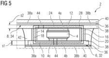
- the first layer of material is designed as a busbar, for example, while the second layer of material is designed as a cooling plate. Furthermore, at least one of the two material layers can be designed as a substrate, in particular as a DCB substrate.
- the semiconductor element is designed, for example, as a vertical semiconductor, in particular as an insulated gate bipolar transistor (IGBT). Other examples of such semiconductor elements include other types of transistors such as field effect transistors, but also triacs, thyristors and diodes, but also, in particular complete, power modules.
- a power module can contain, among other things, a plurality of switches, in particular transistors.
- An example of such a power module is, inter alia, a half-bridge module with at least one half-bridge.
- the semiconductor element 4 can be designed as a, in particular vertical, semiconductor, e.g. as an insulated gate bipolar transistor (IGBT) or another type of transistor, such as a field effect transistor, but also as a triac, thyristor or diode.
- IGBT insulated gate bipolar transistor
- this can, for example, be in contact with the cooling plate on the collector side, while the busbar is connected to the emitter.
- a gate connection can be contacted, among other things, by means of a bond connection or another busbar.
Landscapes
- Cooling Or The Like Of Semiconductors Or Solid State Devices (AREA)
Priority Applications (5)
| Application Number | Priority Date | Filing Date | Title |
|---|---|---|---|
| EP22158230.7A EP4235771A1 (fr) | 2022-02-23 | 2022-02-23 | Dispositif semi-conducteur pourvu d'au moins un élément semi-conducteur, d'une première couche de matière et d'une seconde couche de matière |
| EP22163532.9A EP4235754A1 (fr) | 2022-02-23 | 2022-03-22 | Dispositif à semi-conducteur comprenant un premier élément semi-conducteur et un premier élément de connexion |
| PCT/EP2023/052151 WO2023160949A1 (fr) | 2022-02-23 | 2023-01-30 | Ensemble semi-conducteur comprenant un premier élément semi-conducteur et un premier élément de connexion |
| US18/839,996 US12538801B2 (en) | 2022-02-23 | 2023-01-30 | Semiconductor assembly comprising a first semiconductor element and a first connection element |
| EP23704263.5A EP4441786B1 (fr) | 2022-02-23 | 2023-01-30 | Dispositif semi-conducteur pourvu d'au moins un élément semi-conducteur et d'une première connexion |
Applications Claiming Priority (1)
| Application Number | Priority Date | Filing Date | Title |
|---|---|---|---|
| EP22158230.7A EP4235771A1 (fr) | 2022-02-23 | 2022-02-23 | Dispositif semi-conducteur pourvu d'au moins un élément semi-conducteur, d'une première couche de matière et d'une seconde couche de matière |
Publications (1)
| Publication Number | Publication Date |
|---|---|
| EP4235771A1 true EP4235771A1 (fr) | 2023-08-30 |
Family
ID=80449091
Family Applications (2)
| Application Number | Title | Priority Date | Filing Date |
|---|---|---|---|
| EP22158230.7A Withdrawn EP4235771A1 (fr) | 2022-02-23 | 2022-02-23 | Dispositif semi-conducteur pourvu d'au moins un élément semi-conducteur, d'une première couche de matière et d'une seconde couche de matière |
| EP22163532.9A Withdrawn EP4235754A1 (fr) | 2022-02-23 | 2022-03-22 | Dispositif à semi-conducteur comprenant un premier élément semi-conducteur et un premier élément de connexion |
Family Applications After (1)
| Application Number | Title | Priority Date | Filing Date |
|---|---|---|---|
| EP22163532.9A Withdrawn EP4235754A1 (fr) | 2022-02-23 | 2022-03-22 | Dispositif à semi-conducteur comprenant un premier élément semi-conducteur et un premier élément de connexion |
Country Status (1)
| Country | Link |
|---|---|
| EP (2) | EP4235771A1 (fr) |
Citations (9)
| Publication number | Priority date | Publication date | Assignee | Title |
|---|---|---|---|---|
| US6923362B2 (en) | 2002-09-30 | 2005-08-02 | The Curators Of University Of Missouri | Integral channels in metal components and fabrication thereof |
| US20080224303A1 (en) * | 2006-10-18 | 2008-09-18 | Sunao Funakoshi | Power Semiconductor Module |
| EP2597676A2 (fr) * | 2011-11-28 | 2013-05-29 | Samsung Electro-Mechanics Co., Ltd | Emballage de module de puissance |
| WO2013151606A1 (fr) * | 2012-04-02 | 2013-10-10 | Raytheon Company | Appareil de refroidissement de semi-conducteur |
| WO2018202439A1 (fr) | 2017-05-02 | 2018-11-08 | Siemens Aktiengesellschaft | Module électronique doté d'un composant monté entre deux substrats et procédé pour le fabriquer |
| EP3428964A1 (fr) * | 2016-04-15 | 2019-01-16 | KYOCERA Corporation | Dispositif à semi-conducteurs |
| WO2019015901A1 (fr) | 2017-07-18 | 2019-01-24 | Siemens Aktiengesellschaft | Sous-ensemble électrique et son procédé de fabrication |
| WO2020249479A1 (fr) | 2019-06-11 | 2020-12-17 | Siemens Aktiengesellschaft | Circuit électronique et procédé de fabrication d'un circuit électronique |
| EP3823018A1 (fr) | 2019-11-18 | 2021-05-19 | Siemens Aktiengesellschaft | Module électronique doté d'un caloduc pulsant |
Family Cites Families (2)
| Publication number | Priority date | Publication date | Assignee | Title |
|---|---|---|---|---|
| DE102004057497B4 (de) * | 2004-11-29 | 2012-01-12 | Siemens Ag | Wärmeaustauschvorrichtung und Verfahren zum Herstellen der Wärmeaustauschvorrichtung sowie Anordnung eines Bauelements und der Wärmeaustauschvorrichtung und Verfahren zum Herstellen der Anordnung |
| DE102008063724B4 (de) * | 2007-12-19 | 2012-08-23 | GM Global Technology Operations LLC (n. d. Ges. d. Staates Delaware) | Sammelschienenanordnung mit eingebauter Kühlung, Fahrzeugwechselrichtermodul und Verfahren zum Kühlen eines Wechselrichtermoduls |
-
2022
- 2022-02-23 EP EP22158230.7A patent/EP4235771A1/fr not_active Withdrawn
- 2022-03-22 EP EP22163532.9A patent/EP4235754A1/fr not_active Withdrawn
Patent Citations (9)
| Publication number | Priority date | Publication date | Assignee | Title |
|---|---|---|---|---|
| US6923362B2 (en) | 2002-09-30 | 2005-08-02 | The Curators Of University Of Missouri | Integral channels in metal components and fabrication thereof |
| US20080224303A1 (en) * | 2006-10-18 | 2008-09-18 | Sunao Funakoshi | Power Semiconductor Module |
| EP2597676A2 (fr) * | 2011-11-28 | 2013-05-29 | Samsung Electro-Mechanics Co., Ltd | Emballage de module de puissance |
| WO2013151606A1 (fr) * | 2012-04-02 | 2013-10-10 | Raytheon Company | Appareil de refroidissement de semi-conducteur |
| EP3428964A1 (fr) * | 2016-04-15 | 2019-01-16 | KYOCERA Corporation | Dispositif à semi-conducteurs |
| WO2018202439A1 (fr) | 2017-05-02 | 2018-11-08 | Siemens Aktiengesellschaft | Module électronique doté d'un composant monté entre deux substrats et procédé pour le fabriquer |
| WO2019015901A1 (fr) | 2017-07-18 | 2019-01-24 | Siemens Aktiengesellschaft | Sous-ensemble électrique et son procédé de fabrication |
| WO2020249479A1 (fr) | 2019-06-11 | 2020-12-17 | Siemens Aktiengesellschaft | Circuit électronique et procédé de fabrication d'un circuit électronique |
| EP3823018A1 (fr) | 2019-11-18 | 2021-05-19 | Siemens Aktiengesellschaft | Module électronique doté d'un caloduc pulsant |
Also Published As
| Publication number | Publication date |
|---|---|
| EP4235754A1 (fr) | 2023-08-30 |
Similar Documents
| Publication | Publication Date | Title |
|---|---|---|
| EP4128337B1 (fr) | Module de puissance pourvu d'au moins trois unités de puissance | |
| EP2308274A1 (fr) | Circuit imprimé avec composant électronique | |
| EP3794641B1 (fr) | Dispositif d'évacuation de chaleur pour un module de puissance à semi-conducteurs | |
| EP4275228B1 (fr) | Agencement de module semi-conducteur doté d'un dissipateur thermique et d'au moins un module semi-conducteur | |
| EP3958306A1 (fr) | Module de puissance pourvu d'au moins deux dispositifs de semi-conducteurs de puissance en contact sur un substrat | |
| EP4300574A1 (fr) | Module d'alimentation modulaire | |
| DE4132947C2 (de) | Elektronische Schaltungsanordnung | |
| EP4235771A1 (fr) | Dispositif semi-conducteur pourvu d'au moins un élément semi-conducteur, d'une première couche de matière et d'une seconde couche de matière | |
| EP4012762A1 (fr) | Module semi-conducteur pourvu d'au moins un élément semi-conducteur | |
| EP4211719B1 (fr) | Module semi-conducteur pourvu d'au moins un élément semi-conducteur | |
| EP3940769A1 (fr) | Module semi-conducteur pourvu d'au moins un élément semi-conducteur et d'un substrat | |
| DE102016211479A1 (de) | Leistungsmodul | |
| EP4441786B1 (fr) | Dispositif semi-conducteur pourvu d'au moins un élément semi-conducteur et d'une première connexion | |
| WO2022223237A1 (fr) | Module semi-conducteur comprenant un substrat et au moins un composant semi-conducteur mis en contact sur le substrat | |
| EP4199075A1 (fr) | Module électronique comprenant un caloduc pulsant doté d'une structure de canal | |
| EP4604178A1 (fr) | Dispositif semi-conducteur de puissance comprenant un support de circuit, un dissipateur thermique et un circuit électronique et procédé de fabrication de ce dispositif | |
| DE10249854B4 (de) | Leistungshalbleiter-Baugruppe | |
| EP4682953A1 (fr) | Dispositif semi-conducteur comprenant au moins un élément semi-conducteur, un premier support de circuit et un second support de circuit | |
| EP4128326A2 (fr) | Procédé de mise en contact d'un semi-conducteur de puissance sur un substrat | |
| EP4250340A1 (fr) | Procédé de fabrication d'un dispositif de refroidissement d'un agencement à semi-conducteur comprennant un corps métallique | |
| EP4318554A1 (fr) | Module à semi-conducteur doté d'au moins un premier dispositif à semi-conducteur, d'un second dispositif à semi-conducteur et d'un dissipateur thermique | |
| DE9113276U1 (de) | Elektronische Schaltungsanordnung | |
| EP4665089A1 (fr) | Agencement de circuit | |
| DE102024205618A1 (de) | Durchkontaktierung eines Oberseitensubstrats | |
| EP4546408A1 (fr) | Dispositif semi-conducteur comprenant un premier élément semi-conducteur |
Legal Events
| Date | Code | Title | Description |
|---|---|---|---|
| PUAI | Public reference made under article 153(3) epc to a published international application that has entered the european phase |
Free format text: ORIGINAL CODE: 0009012 |
|
| STAA | Information on the status of an ep patent application or granted ep patent |
Free format text: STATUS: THE APPLICATION HAS BEEN PUBLISHED |
|
| AK | Designated contracting states |
Kind code of ref document: A1 Designated state(s): AL AT BE BG CH CY CZ DE DK EE ES FI FR GB GR HR HU IE IS IT LI LT LU LV MC MK MT NL NO PL PT RO RS SE SI SK SM TR |
|
| STAA | Information on the status of an ep patent application or granted ep patent |
Free format text: STATUS: THE APPLICATION IS DEEMED TO BE WITHDRAWN |
|
| 18D | Application deemed to be withdrawn |
Effective date: 20240301 |