EP4245558A1 - Fälschungssicheres optisches element, herstellungsverfahren dafür und fälschungssicheres produkt - Google Patents
Fälschungssicheres optisches element, herstellungsverfahren dafür und fälschungssicheres produkt Download PDFInfo
- Publication number
- EP4245558A1 EP4245558A1 EP21890989.3A EP21890989A EP4245558A1 EP 4245558 A1 EP4245558 A1 EP 4245558A1 EP 21890989 A EP21890989 A EP 21890989A EP 4245558 A1 EP4245558 A1 EP 4245558A1
- Authority
- EP
- European Patent Office
- Prior art keywords
- area
- layer
- reflective layer
- microstructure
- optical anti
- Prior art date
- Legal status (The legal status is an assumption and is not a legal conclusion. Google has not performed a legal analysis and makes no representation as to the accuracy of the status listed.)
- Pending
Links
- 230000003287 optical effect Effects 0.000 title claims abstract description 87
- 238000004519 manufacturing process Methods 0.000 title claims abstract description 31
- 230000000007 visual effect Effects 0.000 claims abstract description 12
- 239000010410 layer Substances 0.000 claims description 244
- 239000000463 material Substances 0.000 claims description 50
- 238000000576 coating method Methods 0.000 claims description 43
- 239000011241 protective layer Substances 0.000 claims description 30
- 239000000758 substrate Substances 0.000 claims description 29
- 239000011248 coating agent Substances 0.000 claims description 28
- 239000000047 product Substances 0.000 claims description 21
- 239000000049 pigment Substances 0.000 claims description 17
- PXHVJJICTQNCMI-UHFFFAOYSA-N Nickel Chemical compound [Ni] PXHVJJICTQNCMI-UHFFFAOYSA-N 0.000 claims description 12
- 229910052782 aluminium Inorganic materials 0.000 claims description 10
- XAGFODPZIPBFFR-UHFFFAOYSA-N aluminium Chemical compound [Al] XAGFODPZIPBFFR-UHFFFAOYSA-N 0.000 claims description 10
- 239000002245 particle Substances 0.000 claims description 9
- ATJFFYVFTNAWJD-UHFFFAOYSA-N Tin Chemical compound [Sn] ATJFFYVFTNAWJD-UHFFFAOYSA-N 0.000 claims description 8
- 239000011135 tin Substances 0.000 claims description 8
- 229910052718 tin Inorganic materials 0.000 claims description 8
- VYZAMTAEIAYCRO-UHFFFAOYSA-N Chromium Chemical compound [Cr] VYZAMTAEIAYCRO-UHFFFAOYSA-N 0.000 claims description 6
- RYGMFSIKBFXOCR-UHFFFAOYSA-N Copper Chemical compound [Cu] RYGMFSIKBFXOCR-UHFFFAOYSA-N 0.000 claims description 6
- BQCADISMDOOEFD-UHFFFAOYSA-N Silver Chemical compound [Ag] BQCADISMDOOEFD-UHFFFAOYSA-N 0.000 claims description 6
- RTAQQCXQSZGOHL-UHFFFAOYSA-N Titanium Chemical compound [Ti] RTAQQCXQSZGOHL-UHFFFAOYSA-N 0.000 claims description 6
- 238000010521 absorption reaction Methods 0.000 claims description 6
- 229910052804 chromium Inorganic materials 0.000 claims description 6
- 239000011651 chromium Substances 0.000 claims description 6
- 229910052802 copper Inorganic materials 0.000 claims description 6
- 239000010949 copper Substances 0.000 claims description 6
- 229910052759 nickel Inorganic materials 0.000 claims description 6
- 229910052709 silver Inorganic materials 0.000 claims description 6
- 239000004332 silver Substances 0.000 claims description 6
- 239000010936 titanium Substances 0.000 claims description 6
- 229910052719 titanium Inorganic materials 0.000 claims description 6
- VYPSYNLAJGMNEJ-UHFFFAOYSA-N Silicium dioxide Chemical compound O=[Si]=O VYPSYNLAJGMNEJ-UHFFFAOYSA-N 0.000 claims description 4
- GWEVSGVZZGPLCZ-UHFFFAOYSA-N Titan oxide Chemical compound O=[Ti]=O GWEVSGVZZGPLCZ-UHFFFAOYSA-N 0.000 claims description 4
- WMWLMWRWZQELOS-UHFFFAOYSA-N bismuth(iii) oxide Chemical compound O=[Bi]O[Bi]=O WMWLMWRWZQELOS-UHFFFAOYSA-N 0.000 claims description 4
- QDOXWKRWXJOMAK-UHFFFAOYSA-N dichromium trioxide Chemical compound O=[Cr]O[Cr]=O QDOXWKRWXJOMAK-UHFFFAOYSA-N 0.000 claims description 4
- 239000000203 mixture Substances 0.000 claims description 4
- ZKATWMILCYLAPD-UHFFFAOYSA-N niobium pentoxide Chemical compound O=[Nb](=O)O[Nb](=O)=O ZKATWMILCYLAPD-UHFFFAOYSA-N 0.000 claims description 4
- 238000007740 vapor deposition Methods 0.000 claims description 4
- 239000011265 semifinished product Substances 0.000 claims description 3
- 229910009973 Ti2O3 Inorganic materials 0.000 claims description 2
- 241001296405 Tiso Species 0.000 claims description 2
- CETPSERCERDGAM-UHFFFAOYSA-N ceric oxide Chemical compound O=[Ce]=O CETPSERCERDGAM-UHFFFAOYSA-N 0.000 claims description 2
- 229910000422 cerium(IV) oxide Inorganic materials 0.000 claims description 2
- 229910052681 coesite Inorganic materials 0.000 claims description 2
- 229910052906 cristobalite Inorganic materials 0.000 claims description 2
- CJNBYAVZURUTKZ-UHFFFAOYSA-N hafnium(IV) oxide Inorganic materials O=[Hf]=O CJNBYAVZURUTKZ-UHFFFAOYSA-N 0.000 claims description 2
- JEIPFZHSYJVQDO-UHFFFAOYSA-N iron(III) oxide Inorganic materials O=[Fe]O[Fe]=O JEIPFZHSYJVQDO-UHFFFAOYSA-N 0.000 claims description 2
- 229910001635 magnesium fluoride Inorganic materials 0.000 claims description 2
- 230000000737 periodic effect Effects 0.000 claims description 2
- 239000000377 silicon dioxide Substances 0.000 claims description 2
- 229910052950 sphalerite Inorganic materials 0.000 claims description 2
- 229910052682 stishovite Inorganic materials 0.000 claims description 2
- PBCFLUZVCVVTBY-UHFFFAOYSA-N tantalum pentoxide Inorganic materials O=[Ta](=O)O[Ta](=O)=O PBCFLUZVCVVTBY-UHFFFAOYSA-N 0.000 claims description 2
- OGIDPMRJRNCKJF-UHFFFAOYSA-N titanium oxide Inorganic materials [Ti]=O OGIDPMRJRNCKJF-UHFFFAOYSA-N 0.000 claims description 2
- GQUJEMVIKWQAEH-UHFFFAOYSA-N titanium(III) oxide Chemical compound O=[Ti]O[Ti]=O GQUJEMVIKWQAEH-UHFFFAOYSA-N 0.000 claims description 2
- 229910052905 tridymite Inorganic materials 0.000 claims description 2
- 238000005019 vapor deposition process Methods 0.000 claims description 2
- XLOMVQKBTHCTTD-UHFFFAOYSA-N zinc oxide Inorganic materials [Zn]=O XLOMVQKBTHCTTD-UHFFFAOYSA-N 0.000 claims description 2
- 229910052984 zinc sulfide Inorganic materials 0.000 claims description 2
- 238000000034 method Methods 0.000 description 20
- 230000000694 effects Effects 0.000 description 17
- 239000010408 film Substances 0.000 description 15
- 238000005516 engineering process Methods 0.000 description 12
- 238000010586 diagram Methods 0.000 description 10
- 230000008569 process Effects 0.000 description 10
- 238000007639 printing Methods 0.000 description 7
- 229920000139 polyethylene terephthalate Polymers 0.000 description 6
- 239000005020 polyethylene terephthalate Substances 0.000 description 6
- -1 aluminum silver Chemical compound 0.000 description 5
- HEMHJVSKTPXQMS-UHFFFAOYSA-M sodium hydroxide Inorganic materials [OH-].[Na+] HEMHJVSKTPXQMS-UHFFFAOYSA-M 0.000 description 5
- 239000004743 Polypropylene Substances 0.000 description 4
- 238000004806 packaging method and process Methods 0.000 description 4
- 229920001155 polypropylene Polymers 0.000 description 4
- 229920005989 resin Polymers 0.000 description 4
- 239000011347 resin Substances 0.000 description 4
- 239000003086 colorant Substances 0.000 description 3
- PCHJSUWPFVWCPO-UHFFFAOYSA-N gold Chemical compound [Au] PCHJSUWPFVWCPO-UHFFFAOYSA-N 0.000 description 3
- 229910052737 gold Inorganic materials 0.000 description 3
- 239000010931 gold Substances 0.000 description 3
- 238000012986 modification Methods 0.000 description 3
- 230000004048 modification Effects 0.000 description 3
- 229930014626 natural product Natural products 0.000 description 3
- 239000000126 substance Substances 0.000 description 3
- QAOWNCQODCNURD-UHFFFAOYSA-N Sulfuric acid Chemical compound OS(O)(=O)=O QAOWNCQODCNURD-UHFFFAOYSA-N 0.000 description 2
- 239000011230 binding agent Substances 0.000 description 2
- 238000005266 casting Methods 0.000 description 2
- 239000002131 composite material Substances 0.000 description 2
- 239000007788 liquid Substances 0.000 description 2
- 238000000465 moulding Methods 0.000 description 2
- 239000002985 plastic film Substances 0.000 description 2
- 229920006255 plastic film Polymers 0.000 description 2
- 239000011112 polyethylene naphthalate Substances 0.000 description 2
- 239000002994 raw material Substances 0.000 description 2
- 230000002787 reinforcement Effects 0.000 description 2
- 238000007650 screen-printing Methods 0.000 description 2
- 238000000926 separation method Methods 0.000 description 2
- 238000004528 spin coating Methods 0.000 description 2
- 238000005507 spraying Methods 0.000 description 2
- 229920005992 thermoplastic resin Polymers 0.000 description 2
- 239000002253 acid Substances 0.000 description 1
- NIXOWILDQLNWCW-UHFFFAOYSA-N acrylic acid group Chemical group C(C=C)(=O)O NIXOWILDQLNWCW-UHFFFAOYSA-N 0.000 description 1
- 230000003321 amplification Effects 0.000 description 1
- 238000003491 array Methods 0.000 description 1
- 238000006243 chemical reaction Methods 0.000 description 1
- 235000019504 cigarettes Nutrition 0.000 description 1
- 230000008094 contradictory effect Effects 0.000 description 1
- 238000005260 corrosion Methods 0.000 description 1
- 230000007797 corrosion Effects 0.000 description 1
- 239000013039 cover film Substances 0.000 description 1
- 238000003618 dip coating Methods 0.000 description 1
- 239000003814 drug Substances 0.000 description 1
- 229940079593 drug Drugs 0.000 description 1
- 238000005566 electron beam evaporation Methods 0.000 description 1
- 238000010894 electron beam technology Methods 0.000 description 1
- 238000001093 holography Methods 0.000 description 1
- 238000001755 magnetron sputter deposition Methods 0.000 description 1
- 229910052751 metal Inorganic materials 0.000 description 1
- 239000002184 metal Substances 0.000 description 1
- 238000003199 nucleic acid amplification method Methods 0.000 description 1
- 229920000728 polyester Polymers 0.000 description 1
- 229920002635 polyurethane Polymers 0.000 description 1
- 239000004814 polyurethane Substances 0.000 description 1
- 238000003672 processing method Methods 0.000 description 1
- 230000005855 radiation Effects 0.000 description 1
- 238000003847 radiation curing Methods 0.000 description 1
- 230000002285 radioactive effect Effects 0.000 description 1
- 238000007761 roller coating Methods 0.000 description 1
- 229920006395 saturated elastomer Polymers 0.000 description 1
- 239000002904 solvent Substances 0.000 description 1
- 239000004753 textile Substances 0.000 description 1
- 238000002207 thermal evaporation Methods 0.000 description 1
- 230000009466 transformation Effects 0.000 description 1
- 238000000844 transformation Methods 0.000 description 1
Images


Classifications
-
- B—PERFORMING OPERATIONS; TRANSPORTING
- B42—BOOKBINDING; ALBUMS; FILES; SPECIAL PRINTED MATTER
- B42D—BOOKS; BOOK COVERS; LOOSE LEAVES; PRINTED MATTER CHARACTERISED BY IDENTIFICATION OR SECURITY FEATURES; PRINTED MATTER OF SPECIAL FORMAT OR STYLE NOT OTHERWISE PROVIDED FOR; DEVICES FOR USE THEREWITH AND NOT OTHERWISE PROVIDED FOR; MOVABLE-STRIP WRITING OR READING APPARATUS
- B42D25/00—Information-bearing cards or sheet-like structures characterised by identification or security features; Manufacture thereof
- B42D25/30—Identification or security features, e.g. for preventing forgery
- B42D25/324—Reliefs
-
- B—PERFORMING OPERATIONS; TRANSPORTING
- B42—BOOKBINDING; ALBUMS; FILES; SPECIAL PRINTED MATTER
- B42D—BOOKS; BOOK COVERS; LOOSE LEAVES; PRINTED MATTER CHARACTERISED BY IDENTIFICATION OR SECURITY FEATURES; PRINTED MATTER OF SPECIAL FORMAT OR STYLE NOT OTHERWISE PROVIDED FOR; DEVICES FOR USE THEREWITH AND NOT OTHERWISE PROVIDED FOR; MOVABLE-STRIP WRITING OR READING APPARATUS
- B42D25/00—Information-bearing cards or sheet-like structures characterised by identification or security features; Manufacture thereof
- B42D25/30—Identification or security features, e.g. for preventing forgery
- B42D25/328—Diffraction gratings; Holograms
-
- B—PERFORMING OPERATIONS; TRANSPORTING
- B42—BOOKBINDING; ALBUMS; FILES; SPECIAL PRINTED MATTER
- B42D—BOOKS; BOOK COVERS; LOOSE LEAVES; PRINTED MATTER CHARACTERISED BY IDENTIFICATION OR SECURITY FEATURES; PRINTED MATTER OF SPECIAL FORMAT OR STYLE NOT OTHERWISE PROVIDED FOR; DEVICES FOR USE THEREWITH AND NOT OTHERWISE PROVIDED FOR; MOVABLE-STRIP WRITING OR READING APPARATUS
- B42D25/00—Information-bearing cards or sheet-like structures characterised by identification or security features; Manufacture thereof
- B42D25/30—Identification or security features, e.g. for preventing forgery
- B42D25/36—Identification or security features, e.g. for preventing forgery comprising special materials
- B42D25/373—Metallic materials
-
- B—PERFORMING OPERATIONS; TRANSPORTING
- B42—BOOKBINDING; ALBUMS; FILES; SPECIAL PRINTED MATTER
- B42D—BOOKS; BOOK COVERS; LOOSE LEAVES; PRINTED MATTER CHARACTERISED BY IDENTIFICATION OR SECURITY FEATURES; PRINTED MATTER OF SPECIAL FORMAT OR STYLE NOT OTHERWISE PROVIDED FOR; DEVICES FOR USE THEREWITH AND NOT OTHERWISE PROVIDED FOR; MOVABLE-STRIP WRITING OR READING APPARATUS
- B42D25/00—Information-bearing cards or sheet-like structures characterised by identification or security features; Manufacture thereof
- B42D25/30—Identification or security features, e.g. for preventing forgery
- B42D25/36—Identification or security features, e.g. for preventing forgery comprising special materials
- B42D25/378—Special inks
-
- B—PERFORMING OPERATIONS; TRANSPORTING
- B42—BOOKBINDING; ALBUMS; FILES; SPECIAL PRINTED MATTER
- B42D—BOOKS; BOOK COVERS; LOOSE LEAVES; PRINTED MATTER CHARACTERISED BY IDENTIFICATION OR SECURITY FEATURES; PRINTED MATTER OF SPECIAL FORMAT OR STYLE NOT OTHERWISE PROVIDED FOR; DEVICES FOR USE THEREWITH AND NOT OTHERWISE PROVIDED FOR; MOVABLE-STRIP WRITING OR READING APPARATUS
- B42D25/00—Information-bearing cards or sheet-like structures characterised by identification or security features; Manufacture thereof
- B42D25/40—Manufacture
- B42D25/405—Marking
- B42D25/425—Marking by deformation, e.g. embossing
-
- B—PERFORMING OPERATIONS; TRANSPORTING
- B42—BOOKBINDING; ALBUMS; FILES; SPECIAL PRINTED MATTER
- B42D—BOOKS; BOOK COVERS; LOOSE LEAVES; PRINTED MATTER CHARACTERISED BY IDENTIFICATION OR SECURITY FEATURES; PRINTED MATTER OF SPECIAL FORMAT OR STYLE NOT OTHERWISE PROVIDED FOR; DEVICES FOR USE THEREWITH AND NOT OTHERWISE PROVIDED FOR; MOVABLE-STRIP WRITING OR READING APPARATUS
- B42D25/00—Information-bearing cards or sheet-like structures characterised by identification or security features; Manufacture thereof
- B42D25/40—Manufacture
- B42D25/405—Marking
- B42D25/43—Marking by removal of material
-
- B—PERFORMING OPERATIONS; TRANSPORTING
- B42—BOOKBINDING; ALBUMS; FILES; SPECIAL PRINTED MATTER
- B42D—BOOKS; BOOK COVERS; LOOSE LEAVES; PRINTED MATTER CHARACTERISED BY IDENTIFICATION OR SECURITY FEATURES; PRINTED MATTER OF SPECIAL FORMAT OR STYLE NOT OTHERWISE PROVIDED FOR; DEVICES FOR USE THEREWITH AND NOT OTHERWISE PROVIDED FOR; MOVABLE-STRIP WRITING OR READING APPARATUS
- B42D25/00—Information-bearing cards or sheet-like structures characterised by identification or security features; Manufacture thereof
- B42D25/40—Manufacture
- B42D25/45—Associating two or more layers
-
- G—PHYSICS
- G02—OPTICS
- G02B—OPTICAL ELEMENTS, SYSTEMS OR APPARATUS
- G02B5/00—Optical elements other than lenses
- G02B5/08—Mirrors
- G02B5/10—Mirrors with curved faces
-
- G—PHYSICS
- G02—OPTICS
- G02B—OPTICAL ELEMENTS, SYSTEMS OR APPARATUS
- G02B5/00—Optical elements other than lenses
- G02B5/08—Mirrors
- G02B5/09—Multifaceted or polygonal mirrors, e.g. polygonal scanning mirrors; Fresnel mirrors
Definitions
- the present invention relates to the technical field of various types of high-security or high-value-added printed matter such as banknotes, cards and product packaging, in particular to an optical anti-counterfeiting element and a manufacturing method thereof, and an anti-counterfeiting product with the anti-counterfeiting element.
- optical anti-counterfeiting elements such as security threads, bars or labels are widely used in various types of high-security or high-value-added printed matter such as banknotes, cards and product packaging.
- a variety of anti-counterfeiting technologies are adopted for the optical anti-counterfeiting elements.
- holographic anti-counterfeiting technology is the most common anti-counterfeiting technology at present, for example, windowed security threads of China's fifth RMB series (2005 edition) except for 1-yuan banknotes, and ID cards, driving licenses, passports and other important documents in China.
- this technology has also been widely used in the civil packaging industry, such as packaging of cigarettes, wine and drugs, and even labels of textiles and toys have adopted this technology, which also makes the anti-counterfeiting performance of this technology worse and worse.
- the anti-counterfeiting industry has great interest in this new-type micro lens array technology, which is an anti-counterfeiting technology with dynamic features or with a depth-of-field effect based on a Moire amplification effect of a micro lens array on a micrographic array, that is, the micro lens array may sample and synthesize the micrographic array to form an image.
- This technology requires sufficient contrast in color or brightness between a micrographic area and a micrographic background area.
- the patent document CN200680062431.9 discloses a method of producing micrographics by squeegeeing, that is, an undulating structure layer with an iconic depression structure is formed firstly, and is then integrally coated with radiation-curable ink with a certain thickness, then ink outside the depression structure is removed with a squeegee, and finally the radiation-curable ink in the depression structure is radiation-cured with a certain dose of radiation source.
- the difficulty of this method is that it is difficult for the squeegee to remove ink from the micrographic background area completely, in particular, for large-width film rolls (for example, being 1m wide), it is difficult to control the lateral uniformity.
- the method may only achieve manufacturing of micrographics with particular colors, but not micrographics that present different color features depending on a viewing angle.
- the patent document US20030179364 discloses manufacturing of black micrographics using microstructures with a high depth-to-width ratio. This method is simple in process and highly feasible, but poor in color effect, and may not achieve producing of color graphics with high brightness and high saturation or color-shifting micrographics.
- an object of the present invention is to provide an optical anti-counterfeiting element, a manufacturing method thereof, and an anti-counterfeiting product.
- the optical anti-counterfeiting element includes: an undulating structure layer, a surface of the undulating structure layer is in an undulating shape.
- the undulating structure layer includes at least two areas, and different reflective layers are correspondingly arranged in the areas on the surface in the undulating shape, such that when observing from the other surface of the undulating structure layer, the different areas present visual features of the corresponding reflective layers.
- the undulating structure layer includes: a first area, including a first microstructure; and a second area, including a second microstructure.
- the first area is provided with a first reflective layer
- the second area is provided with a second reflective layer, such that when observing from the other surface of the undulating structure layer, the first area has visual features presented by the first reflective layer, and the second area has visual features presented by the second reflective layer.
- At least one of the first area and the second area includes a pattern with a line or a dot, and a width of the line or a diameter of the dot is less than 0.25mm.
- the first reflective layer is located in the first area, and the second reflective layer is located at least in the second area.
- a specific volume of the first microstructure is less than a specific volume of the second microstructure.
- the first microstructure or the second microstructure is: at least one of a periodic structure and an aperiodic structure; and a cross-sectional structure of the first microstructure or the second microstructure along an extension direction is: at least one of a sinusoidal structure, a rectangular grating structure, a trapezoidal grating structure, a blazed grating structure and an arc grating structure.
- the specific volume of the first microstructure ranges from 0 ⁇ m 3 / ⁇ m 2 to 0.5 ⁇ m 3 / ⁇ m 2 ; and the specific volume of the second microstructure ranges from 0.4 ⁇ m 3 / ⁇ m 2 to 2 ⁇ m 3 / ⁇ m 2 .
- the first reflective layer is formed by a vapor deposition process, and a material of the first reflective layer is at least one of aluminum, silver, copper, tin, chromium, nickel and titanium.
- a thickness of the first reflective layer ranges from 10nm to 80nm.
- the first reflective layer is a multilayer interference optically variable coating.
- the second reflective layer or a sublayer of the second reflective layer is formed by a wet coating process.
- the multilayer interference optically variable coating includes a mirror layer, a dielectric layer and an absorption layer, and the absorption layer is arranged adjacent to the undulating structure layer; a material of the mirror layer includes at least one of aluminum, silver, copper, tin, chromium, nickel and titanium; a material of the dielectric layer includes at least one of MgF 2 , SiO 2 , ZnS, TiN, TiO 2 , TiO, Ti 2 O 3 , TisOs, Ta 2 O 5 , Nb 2 O 5 , CeO 2 , Bi 2 O 3 , Cr 2 O 3 , Fe 2 O 3 , HfO 2 and ZnO; and the absorption layer includes at least one of nickel, chromium, aluminum, silver, copper, tin and titanium.
- the second reflective layer is a coating formed by a metallic ink.
- the metallic ink is an optically variable ink.
- the second reflective layer is a coating formed by a mixture of the metallic ink and a color pigment.
- a metallic pigment of the metallic ink is an aluminum microchip.
- an average diameter of a pigment flake particle of the metallic ink is less than a width of a cross-section of the second microstructure.
- the average diameter of the pigment flake particle of the metallic ink is less than 10 ⁇ m.
- the second reflective layer is a multilayer structure, and includes a color ink layer sublayer and a reflective layer sublayer, and the color ink layer sublayer is formed by a wet coating process.
- a surface of a color ink layer away from the undulating structure layer corresponds to the undulating shape of the surface of the undulating structure layer.
- the color ink layer sublayer is applied in an amount ranging from 0.1g/m 2 to 1g/m 2 .
- the anti-counterfeiting product includes the above-mentioned optical anti-counterfeiting element.
- the manufacturing method includes: forming an undulating structure layer, the undulating structure layer at least includes a first area formed by a first microstructure, and a second area formed by a second microstructure, a specific volume of the first microstructure is less than a specific volume of the second microstructure; forming a first reflective layer located in the first area but not in the second area; and forming a second reflective layer located at least in the second area, the second reflective layer or a sublayer of the second reflective layer is formed by a wet coating process.
- the forming the first reflective layer located in the first area but not in the second area further includes: forming a material of the first reflective layer on the undulating structure layer by a vapor deposition; forming a protective layer on the material of the first reflective layer; and placing an obtained semi-finished product into an atmosphere capable of reacting with the material of the first reflective layer to remove all or a part of the material of the first reflective layer located in the second area.
- the manufacturing method further includes: continuing a procedure of applying other inorganic or organic coatings to achieve other optical anti-counterfeiting functions or assisting functions.
- the embodiments of the present invention mainly provide the optical anti-counterfeiting element, the optical anti-counterfeiting element is partitioned by the undulating structure layer, and different reflective layers are correspondingly arranged in the corresponding areas, such that when observing from the other surface of the undulating structure layer by users, different areas present visual features of the corresponding reflective layers, thereby improving anti-counterfeiting capability.
- Embodiment 1 of the present invention provides shape features of an optical anti-counterfeiting element, and it should be understood that this embodiment serves only as an example for the optical anti-counterfeiting element, and does not limit the appearance and specific graphic content of the optical anti-counterfeiting element.
- Fig. 1 is a top view of an optical anti-counterfeiting element according to the present invention.
- the optical anti-counterfeiting element includes a first area A presenting an effect of a first reflective layer, and a second area B presenting an effect of a second reflective layer.
- the first area A presents an aluminum silver color
- the second area B presents a gold color.
- the first area A has a particular optical effect presented by a first microstructure
- the second area B has another particular optical effect presented by a second microstructure.
- first area A and the second area B are distinguished based on the first microstructure and the second microstructure, as illustrated in the following embodiments, which is not illustrated too much in the embodiment of the present invention.
- the first area A and the second area B are presented by means of a preset pattern or image background, the pattern is presented in a form of including a line or a dot, or a combination of both.
- the second area B is letters of "PY" having an embossed optical effect.
- an anti-counterfeiting effect is increased by improving a fineness of an image line, for example, the image line is less than 0.25mm, or even less than 0.05mm.
- the first area A is also set with other optical effects, such as holography, to be visually distinguished from the second area B, thereby increasing the anti-counterfeiting effect.
- Embodiment 2 of the present invention provides a specific structural composition of the optical anti-counterfeiting element.
- Fig. 2 is a cross-sectional view of the optical anti-counterfeiting element shown in Fig. 1 along X-X according to the embodiment of the present invention.
- the optical anti-counterfeiting element includes an undulating structure layer 2, a surface of the undulating structure layer 2 is in an undulating shape. Specifically, a back side of user vision is in the undulating shape, that is, a side of the optical anti-counterfeiting element is in the undulating shape away from the user vision.
- the undulating structure layer 2 includes at least two areas, and different reflective layers are correspondingly arranged in the areas on the undulating surface in the undulating shape, such that when observing from the other surface of the undulating structure layer 2, the different areas present visual features of the corresponding reflective layers.
- the undulating structure layer 2 includes two areas corresponding to Embodiment 1, that is, a first area A formed by a first microstructure (for example, a microstructure presenting a holographic effect), and a second area B adjacent to the first area and formed by a second microstructure (for example, a microstructure presenting an embossed effect).
- a specific volume of the first microstructure is less than a specific volume of the second microstructure.
- the specific volume refers to a volume occupied by a substance per unit mass.
- the first microstructure included in the first area A occupies a smaller volume per unit mass than the second microstructure, but specific shapes and percentages of the first area A and the second area B are not predetermined and are set according to product requirements.
- the optical anti-counterfeiting element further includes a first reflective layer 3 corresponding to the first area A, and a second reflective layer 5 corresponding to the second area B.
- first reflective layer 3 When observing from a non-undulating side of the undulating structure layer 2, the first reflective layer 3 is strictly located in the first area A, and the second reflective layer 5 is strictly located in the second area B.
- the first area A of the undulating structure layer 2 presents optical features of the first reflective layer 3 and the second area B presents optical features of the second reflective layer 5.
- the second reflective layer 5 is a metallic ink coating with a different visual effect from the first reflective layer 3, and the metallic ink coating is formed by a wet coating process.
- the metallic ink coating generally includes a metallic flake particle pigment (for example, a metallic pigment presenting a gold color) and a resin binder.
- the metallic flake particle pigment is basically parallel to an inclined plane of the second microstructure, so that a desired microstructure optical effect is able to be formed.
- the second reflective layer 5 is a result of natural leveling of liquid ink applied to the undulating structure layer, that is, an undulating shape of a surface of the second reflective layer 5 is basically the same as an undulating shape of a surface of the undulating structure layer 2 at the corresponding position.
- an undulating degree of the second reflective layer 5 is set to be less than an undulating degree of the surface of the undulating structure layer 2.
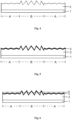
- Fig. 3 is another cross-sectional view of the optical anti-counterfeiting element shown in Fig. 2 along X-X.
- the optical anti-counterfeiting element further includes:
- the substrate layer 1 is at least partially transparent, or a colored dielectric layer, or a transparent dielectric film with a functional coating on a surface, or a composite multilayer film.
- the substrate layer 1 is formed by a film material with good physical and chemical resistance and high mechanical strength.
- a polyethylene terephthalate (PET) film, a polyethylene naphthalate (PEN) film, a polypropylene (PP) film and other plastic films are configured to form the substrate layer 1.
- the substrate layer 1 is formed by the PET material.
- a bonding reinforcement layer (not shown) is arranged between the substrate layer 1 and the undulating structure layer 2 to enhance bonding between the substrate layer 1 and the undulating structure layer 2, and a release layer (not shown) is also arranged therebetween to facilitate separation of the substrate layer 1 from the undulating structure layer 2.
- the protective layer 4 is a natural product of the product manufacturing process.
- Other functional coatings 6 are provided as needed, for example, a bonding layer for bonding with an applicable main product or a protective layer for protection, or a layer for both protection and bonding.
- a manufacturing method of the optical anti-counterfeiting element according to Embodiment 2 of the present invention is described with reference to a flowchart illustration, and it will be appreciated by those skilled in the art that the manufacturing method includes steps S1 to S3.
- Fig. 4 is a structural schematic diagram of step S1 of the manufacturing method of the optical anti-counterfeiting element according to the embodiment of the present invention.
- the undulating structure layer 2 is made by a jig for fixing the substrate layer 1.
- the substrate layer 1 is at least partially transparent, or a colored dielectric layer, or a transparent dielectric film with a functional coating on a surface, or a composite multilayer film.
- the substrate layer 1 is generally formed by a film material with good physical and chemical resistance and high mechanical strength.
- a polyethylene terephthalate (PET) film, a polyethylene naphthalate (PEN) film, a polypropylene (PP) film and other plastic films are configured to form the substrate layer 1.
- the substrate layer 1 is formed by the PET material.
- the substrate layer 1 includes a bonding reinforcement layer to enhance the bonding between the substrate layer 1 and the undulating structure layer 2, and also includes a release layer to facilitate separation of the substrate layer 1 from the undulating structure layer 2.
- the undulating structure layer 2 is duplicated in batches by UV casting, molding, nanoimprinting, and other processing methods.
- the undulating structure layer 2 is formed from thermoplastic resin by a molding process, that is, the thermoplastic resin pre-printed on the substrate layer 1 is softened and deformed by heat when passing through a high-temperature metal stencil so as to form a particular undulating structure, and is then cooled and molded.
- the undulating structure layer 2 is also formed by a radiation-curing casting process, that is, radiation-curable resin is printed on the substrate layer 1, and an original plate is pushed onto the substrate layer while the substrate layer is irradiated with radioactive rays such as ultraviolet light or electron beams, so that the above material is cured, then the original plate is removed, and the undulating structure layer 2 is formed.
- a radiation-curing casting process that is, radiation-curable resin is printed on the substrate layer 1, and an original plate is pushed onto the substrate layer while the substrate layer is irradiated with radioactive rays such as ultraviolet light or electron beams, so that the above material is cured, then the original plate is removed, and the undulating structure layer 2 is formed.
- the undulating structure layer 2 at least includes a first area A formed by a first microstructure, and a second area B adjacent to the first area and formed by a second microstructure.
- a specific volume of the first microstructure is less than a specific volume of the second microstructure. Shapes and specific structure parameters of the first microstructure and the second microstructure are set based on a desired optical effect.
- a cross-section thereof is a blazed grating structure with a variable width of 2 ⁇ m to 20 ⁇ m and a specific volume of about 1 ⁇ m 3 / ⁇ m 2 ; and if the second microstructure is an optical microstructure with a holographic effect, a cross-section thereof is a sinusoidal grating structure with a specific volume of about 0.1 ⁇ m 3 / ⁇ m 2 .
- Fig. 5 is a structural schematic diagram of step S2 of the manufacturing method of the optical anti-counterfeiting element according to the embodiment of the present invention.
- the first reflective layer 3 located in the first area A but not in the second area B.
- a vapor deposition method specifically includes, but is not limited to, thermal evaporation, electron beam evaporation, magnetron sputtering, etc.
- the material of the first reflective layer 3 is formed on the undulating structure layer 2 with a uniform surface density in a homotypically located or basically homotypically located manner.
- the material of the first reflective layer 3 is aluminum, with a thickness of 30nm.
- Fig. 6 is a structural schematic diagram of step S2-2 of the manufacturing method of the optical anti-counterfeiting element according to the embodiment of the present invention.
- the step of forming, in the first area, a first reflective layer located in the first area further includes: S2-2: Forming a material of a protective layer 4 on the material of the first reflective layer 3, as shown in Fig. 6
- the material of the protective layer 4 is generally formed by a wet coating process. In term of a forming area, the material of the protective layer is able to be formed within the whole area of a film (referred to as a coating process), or within a local area of the film (referred to as a printing process). In terms of specific implementation technology, there are spraying, roller coating, spin coating, flexographic printing, intaglio printing, screen printing, etc.
- the protective layer 4 plays a role in protecting the material of the first reflective layer 3 in the image area A in a hollowing process.
- the material of the protective layer 4 needs to be applied in such an amount that the minimum thickness of the material of the protective layer on the material of the first reflective layer 3 in the image area A is significantly less than that of the material of the protective layer on the material of the first reflective layer 3 in the hollowed-out area B.
- a position, with the minimum thickness, of a coating is located on the top of a microstructure.
- the material of the protective layer 4 is applied generally in an amount of greater than 0.1 g/m 2 and less than 0.5 g/m 2 .
- the protective layer 4 provides effective protection for the material of the first reflective layer 3 in the image area A, but not for the material of the first reflective layer 3 in the hollowed-out area B.
- Main resin of the protective layer 4 is formed by polyurethane, acrylic, polyester, or a combination thereof.
- Fig. 7 is a structural schematic diagram of step S2-3 of the manufacturing method of the optical anti-counterfeiting element according to the embodiment of the present invention.
- the step of forming, in the first area, a first reflective layer located in the first area further includes: S2-3: Placing a semi-finished product obtained in S2-2 into an atmosphere capable of reacting with the material of the first reflective layer 3 to remove all or a part of the material of the first reflective layer 3 located in the second area B, as shown in Fig. 7 .
- the minimum thickness of the material of the protective layer 4 on the material of the first reflective layer 3 in the image area A is significantly less than that of the material of the protective layer on the material of the first reflective layer 3 in the hollowed-out area B.
- the corrosive atmosphere capable of reacting with the material of the first reflective layer 3
- the corrosive atmosphere reaches the material of the first reflective layer 3 below through a weak point (that is, corresponding to the top of the microstructure) of the material of the protective layer 4 in the hollowed-out area B, and carries out a corrosion reaction on the material of the first reflective layer.
- the material of the protective layer 4 located in image area A effectively protects the material of the first reflective layer 3 below.
- the first reflective layer 3 located precisely in the first area A is obtained.
- the material of the first reflective layer 3 is aluminum
- the corrosive atmosphere is lye or acid, for example, an NaOH solution or a sulfuric acid solution.
- Fig. 8 is a structural schematic diagram of step S3 of the manufacturing method of the optical anti-counterfeiting element according to the embodiment of the present invention.
- the manufacturing method further includes: S3: Forming a second reflective layer 5 located at least in the second area B, the second reflective layer 5 is formed by a wet coating process.
- the second reflective layer 5 is a metallic ink coating.
- a raw material of the metallic ink coating is a liquid metallic ink formed by a metallic flake particle pigment (for example, a metallic pigment presenting a gold color), a resin binder, and a solvent.
- the wet coating process is intaglio coating, spray coating, dip coating, spin coating, intaglio printing, flexographic printing, screen printing, undulating printing, etc.
- a local printing process is adopted, that is, the second reflective layer 5 is formed merely in the second area B and a small part of the first area surrounding the second area B.
- the metallic flake particle pigment is basically parallel to an inclined plane of the second microstructure, so that a desired microstructure optical effect may be formed.
- An embodiment of the present invention further provides a post-treatment process following step S3, that is, a functional coating 6 is applied as required, for example, a bonding layer for bonding with a main product.
- Fig. 9 is another cross-sectional view of the exemplary optical anti-counterfeiting element shown in Fig. 1 along X-X according to Embodiment 2 of the present invention.
- the optical anti-counterfeiting element includes a substrate layer 1, an undulating structure layer 2, a first reflective layer 3, a protective layer 4, a second reflective layer 5, and the functional coating 6.
- the undulating structure layer 2 at least includes a first area A formed by a first microstructure (for example, a microstructure presenting a holographic effect), and a second area B adjacent to the first area and formed by a second microstructure (for example, a microstructure presenting an embossed effect).
- a specific volume of the first microstructure is less than a specific volume of the second microstructure.
- the first reflective layer 3 is strictly located in the first area A
- the second reflective layer 5 is strictly located in the second area B.
- the second reflective layer 5 is a coating with a different visual effect from the first reflective layer 3, and is formed by a wet coating process.
- the second reflective layer 5 is a coating of a mixture of a metallic ink and a color pigment. Compared with a single metallic ink in Embodiment 1, the color pigment provides rich selections of colors for the reflective layer, thereby having a better visual effect.
- the metallic flake particle pigment is basically parallel to an inclined plane of the second microstructure, so that a desired microstructure optical effect is ensured.
- the protective layer 4 is a natural product of the product manufacturing process.
- the functional coating 6 is provided as needed, for example, a bonding layer for bonding with a main product.
- Fig. 10 is another cross-sectional view of the optical anti-counterfeiting element shown in Fig. 1 along X-X according to Embodiment 3 of the present invention.
- the optical anti-counterfeiting element includes a substrate layer 1, an undulating structure layer 2, a first reflective layer 3, a protective layer 4, a second reflective layer 5 (including a color sublayer 51 of the second reflective layer and a reflective sublayer 52 of the second reflective layer), and a functional coating 6.
- the undulating structure layer 2 at least includes a first area A formed by a first microstructure (for example, a microstructure presenting a holographic effect), and a second area B adjacent to the first area and formed by a second microstructure (for example, a microstructure presenting an embossed effect).
- a specific volume of the first microstructure is less than a specific volume of the second microstructure.
- the first reflective layer 3 is strictly located in the first area A
- the second reflective layer 5 is strictly located in the second area B.
- the color sublayer 51 of the second reflective layer 5 provides rich selections of highly saturated colors for the reflective layer
- the reflective sublayer 52 of the second reflective layer 5 provides a high-brightness reflection function.
- the multilayer second reflective layer 5 has higher brightness and color saturation, thereby having a better visual effect.
- the protective layer 4 is a natural product of the product manufacturing process.
- the functional coating 6 is provided as needed, for example, a bonding layer for bonding with a main product.
- the manufacturing method of the optical anti-counterfeiting element according to the present invention is suitable for manufacturing a windowed security thread, a label, a logo, a wide strip, a transparent window, a cover film, etc.
- Security paper with the windowed security thread is configured to prevent counterfeiting of banknotes, passports, securities and other high-security products.
- An embodiment of the present invention further provides an anti-counterfeiting product.
- the anti-counterfeiting product includes the above-mentioned optical anti-counterfeiting element.
- the optical anti-counterfeiting element is transferred or pasted to the anti-counterfeiting product in the form of a logo, a hot-stamped wide strip, a sticker, a security thread, etc. to achieve an anti-counterfeiting effect.
Landscapes
- Engineering & Computer Science (AREA)
- Manufacturing & Machinery (AREA)
- Physics & Mathematics (AREA)
- General Physics & Mathematics (AREA)
- Optics & Photonics (AREA)
- Credit Cards Or The Like (AREA)
Applications Claiming Priority (2)
| Application Number | Priority Date | Filing Date | Title |
|---|---|---|---|
| CN202011255955.3A CN114475043B (zh) | 2020-11-11 | 2020-11-11 | 光学防伪元件及其制作方法、防伪产品 |
| PCT/CN2021/127488 WO2022100462A1 (zh) | 2020-11-11 | 2021-10-29 | 光学防伪元件及其制作方法、防伪产品 |
Publications (2)
| Publication Number | Publication Date |
|---|---|
| EP4245558A1 true EP4245558A1 (de) | 2023-09-20 |
| EP4245558A4 EP4245558A4 (de) | 2024-04-24 |
Family
ID=81490792
Family Applications (1)
| Application Number | Title | Priority Date | Filing Date |
|---|---|---|---|
| EP21890989.3A Pending EP4245558A4 (de) | 2020-11-11 | 2021-10-29 | Fälschungssicheres optisches element, herstellungsverfahren dafür und fälschungssicheres produkt |
Country Status (3)
| Country | Link |
|---|---|
| EP (1) | EP4245558A4 (de) |
| CN (1) | CN114475043B (de) |
| WO (1) | WO2022100462A1 (de) |
Family Cites Families (17)
| Publication number | Priority date | Publication date | Assignee | Title |
|---|---|---|---|---|
| AUPQ146199A0 (en) * | 1999-07-07 | 1999-07-29 | Note Printing Australia Limited | Improved security document or device |
| HK1044960A1 (zh) * | 1999-10-19 | 2002-11-08 | Rolic Ag | 拓撲結構化的聚合物塗層 |
| US7221512B2 (en) | 2002-01-24 | 2007-05-22 | Nanoventions, Inc. | Light control material for displaying color information, and images |
| FR2982038B1 (fr) * | 2011-10-28 | 2013-11-15 | Hologram Ind | Composant optique de securite a effet reflectif, fabrication d'un tel composant et document securise equipe d'un tel composant |
| FR3000112B1 (fr) * | 2012-12-20 | 2015-03-06 | Arjowiggins Security | Structure de securite. |
| CN103963510B (zh) * | 2013-01-29 | 2015-12-23 | 中钞特种防伪科技有限公司 | 一种制备光学防伪元件的方法 |
| CN104647934B (zh) * | 2013-11-21 | 2016-10-05 | 中钞特种防伪科技有限公司 | 一种光学防伪元件及其制作方法 |
| CN104647938B (zh) * | 2013-11-22 | 2016-03-23 | 中钞特种防伪科技有限公司 | 一种制备光学防伪元件的方法 |
| CN106891637B (zh) * | 2015-12-17 | 2018-12-21 | 中钞特种防伪科技有限公司 | 光学防伪元件及其制备方法 |
| CN107379814B (zh) * | 2017-08-31 | 2018-04-13 | 霍辰尧 | 防伪文件及其制造方法和安全票证 |
| CN109895526B (zh) * | 2017-12-08 | 2021-06-22 | 中钞特种防伪科技有限公司 | 光学防伪元件及其制作方法 |
| DE102018004089A1 (de) * | 2018-05-18 | 2019-11-21 | Giesecke+Devrient Currency Technology Gmbh | Sicherheitselement mit bereichsweise metallisiertem Flächenbereich, Herstellungsverfahren und Prägewerkzeug |
| CN110712452B (zh) * | 2018-07-13 | 2021-03-12 | 中钞特种防伪科技有限公司 | 光学防伪元件及其制备方法和光学防伪产品 |
| CN111746171B (zh) * | 2019-03-29 | 2021-06-15 | 中钞特种防伪科技有限公司 | 光学防伪元件及其制作方法 |
| CN111746172B (zh) * | 2019-03-29 | 2021-11-12 | 中钞特种防伪科技有限公司 | 双面异色光学防伪元件及其制作方法 |
| CN111823749B (zh) * | 2019-04-19 | 2022-02-25 | 中钞特种防伪科技有限公司 | 光学防伪元件及其制作方法、光学防伪产品 |
| CN111890817B (zh) * | 2019-05-05 | 2022-03-22 | 中钞特种防伪科技有限公司 | 多层镀层光学防伪元件及其制作方法 |
-
2020
- 2020-11-11 CN CN202011255955.3A patent/CN114475043B/zh active Active
-
2021
- 2021-10-29 EP EP21890989.3A patent/EP4245558A4/de active Pending
- 2021-10-29 WO PCT/CN2021/127488 patent/WO2022100462A1/zh not_active Ceased
Also Published As
| Publication number | Publication date |
|---|---|
| EP4245558A4 (de) | 2024-04-24 |
| WO2022100462A1 (zh) | 2022-05-19 |
| CN114475043B (zh) | 2023-04-28 |
| CN114475043A (zh) | 2022-05-13 |
Similar Documents
| Publication | Publication Date | Title |
|---|---|---|
| JP5037863B2 (ja) | 隠しセキュリティ・コーティング | |
| CN101824776B (zh) | 防伪装置 | |
| RU2641864C2 (ru) | Оптически изменяющиеся защитные нити и полоски | |
| US7625632B2 (en) | Alignable diffractive pigment flakes and method and apparatus for alignment and images formed therefrom | |
| DE60024827T2 (de) | Diffraktionsfläche mit hintergrund aus wechselenden farben | |
| RU2676011C2 (ru) | Оптически изменяющиеся магнитные защитные нити и полоски | |
| CN102186677B (zh) | 印刷安全特征的改进 | |
| US20080088895A1 (en) | Article With Micro Indicia Security Enhancement | |
| US8067056B2 (en) | Method for producing tamper-proof identification elements | |
| CN109895526B (zh) | 光学防伪元件及其制作方法 | |
| US20110091665A1 (en) | Security element having a screened layer composed of grid elements | |
| US20150258837A1 (en) | Optically variable security threads and stripes | |
| CA2769036A1 (en) | Transfer foil comprising optically variable magnetic pigment, method of making, use of transfer foil, and article or document comprising such | |
| US20060275625A1 (en) | High and low refractive index and metallic surface relief coatings | |
| KR100429414B1 (ko) | 다층재료및그제조방법 | |
| JP2009063703A (ja) | 偽造防止積層体、偽造防止転写箔、偽造防止シール、偽造防止媒体、およびこれらの製造方法 | |
| US20080054623A1 (en) | Printed Article With Special Effect Coating | |
| CN110712451B (zh) | 光学防伪元件及其制备方法和光学防伪产品 | |
| CN111746172B (zh) | 双面异色光学防伪元件及其制作方法 | |
| US20080019003A1 (en) | Vacuum Roll Coated Security Thin Film Interference Products With Overt And/Or Covert Patterned Layers | |
| CN114746282B (zh) | 装饰膜、制造装饰膜的方法和装饰目标基材的方法 | |
| EP4245558A1 (de) | Fälschungssicheres optisches element, herstellungsverfahren dafür und fälschungssicheres produkt | |
| EP3055457B1 (de) | Optisch variable sicherheitsfäden und -streifen | |
| RU2459710C2 (ru) | Защитное устройство, содержащее связующий материал с изменяющимися оптическими свойствами | |
| DE68927899T2 (de) | Bebilderte Prägefolie für Wärmeübertragung, Artikel und Verfahren |
Legal Events
| Date | Code | Title | Description |
|---|---|---|---|
| STAA | Information on the status of an ep patent application or granted ep patent |
Free format text: STATUS: THE INTERNATIONAL PUBLICATION HAS BEEN MADE |
|
| PUAI | Public reference made under article 153(3) epc to a published international application that has entered the european phase |
Free format text: ORIGINAL CODE: 0009012 |
|
| STAA | Information on the status of an ep patent application or granted ep patent |
Free format text: STATUS: REQUEST FOR EXAMINATION WAS MADE |
|
| 17P | Request for examination filed |
Effective date: 20230609 |
|
| AK | Designated contracting states |
Kind code of ref document: A1 Designated state(s): AL AT BE BG CH CY CZ DE DK EE ES FI FR GB GR HR HU IE IS IT LI LT LU LV MC MK MT NL NO PL PT RO RS SE SI SK SM TR |
|
| DAV | Request for validation of the european patent (deleted) | ||
| DAX | Request for extension of the european patent (deleted) | ||
| A4 | Supplementary search report drawn up and despatched |
Effective date: 20240326 |
|
| RIC1 | Information provided on ipc code assigned before grant |
Ipc: B42D 25/40 20140101ALI20240320BHEP Ipc: B42D 25/324 20140101ALI20240320BHEP Ipc: B42D 25/328 20140101ALI20240320BHEP Ipc: B42D 25/30 20140101AFI20240320BHEP |