EP4529369A1 - Verfahren zur herstellung von mindestens einer leitfähigen strukturschicht auf oder in einem komponententräger - Google Patents
Verfahren zur herstellung von mindestens einer leitfähigen strukturschicht auf oder in einem komponententräger Download PDFInfo
- Publication number
- EP4529369A1 EP4529369A1 EP23198894.0A EP23198894A EP4529369A1 EP 4529369 A1 EP4529369 A1 EP 4529369A1 EP 23198894 A EP23198894 A EP 23198894A EP 4529369 A1 EP4529369 A1 EP 4529369A1
- Authority
- EP
- European Patent Office
- Prior art keywords
- structure layer
- conductive structure
- conductive
- electric
- model
- Prior art date
- Legal status (The legal status is an assumption and is not a legal conclusion. Google has not performed a legal analysis and makes no representation as to the accuracy of the status listed.)
- Withdrawn
Links
Images
Classifications
-
- H—ELECTRICITY
- H05—ELECTRIC TECHNIQUES NOT OTHERWISE PROVIDED FOR
- H05K—PRINTED CIRCUITS; CASINGS OR CONSTRUCTIONAL DETAILS OF ELECTRIC APPARATUS; MANUFACTURE OF ASSEMBLAGES OF ELECTRICAL COMPONENTS
- H05K3/00—Apparatus or processes for manufacturing printed circuits
- H05K3/22—Secondary treatment of printed circuits
- H05K3/225—Correcting or repairing of printed circuits
-
- G—PHYSICS
- G06—COMPUTING OR CALCULATING; COUNTING
- G06N—COMPUTING ARRANGEMENTS BASED ON SPECIFIC COMPUTATIONAL MODELS
- G06N3/00—Computing arrangements based on biological models
- G06N3/02—Neural networks
- G06N3/08—Learning methods
-
- H—ELECTRICITY
- H05—ELECTRIC TECHNIQUES NOT OTHERWISE PROVIDED FOR
- H05K—PRINTED CIRCUITS; CASINGS OR CONSTRUCTIONAL DETAILS OF ELECTRIC APPARATUS; MANUFACTURE OF ASSEMBLAGES OF ELECTRICAL COMPONENTS
- H05K1/00—Printed circuits
- H05K1/02—Details
- H05K1/0286—Programmable, customizable or modifiable circuits
- H05K1/0293—Individual printed conductors which are adapted for modification, e.g. fusable or breakable conductors, printed switches
-
- H—ELECTRICITY
- H05—ELECTRIC TECHNIQUES NOT OTHERWISE PROVIDED FOR
- H05K—PRINTED CIRCUITS; CASINGS OR CONSTRUCTIONAL DETAILS OF ELECTRIC APPARATUS; MANUFACTURE OF ASSEMBLAGES OF ELECTRICAL COMPONENTS
- H05K3/00—Apparatus or processes for manufacturing printed circuits
- H05K3/0005—Apparatus or processes for manufacturing printed circuits for designing circuits by computer
-
- B—PERFORMING OPERATIONS; TRANSPORTING
- B23—MACHINE TOOLS; METAL-WORKING NOT OTHERWISE PROVIDED FOR
- B23K—SOLDERING OR UNSOLDERING; WELDING; CLADDING OR PLATING BY SOLDERING OR WELDING; CUTTING BY APPLYING HEAT LOCALLY, e.g. FLAME CUTTING; WORKING BY LASER BEAM
- B23K26/00—Working by laser beam, e.g. welding, cutting or boring
- B23K26/351—Working by laser beam, e.g. welding, cutting or boring for trimming or tuning of electrical components
-
- H—ELECTRICITY
- H05—ELECTRIC TECHNIQUES NOT OTHERWISE PROVIDED FOR
- H05K—PRINTED CIRCUITS; CASINGS OR CONSTRUCTIONAL DETAILS OF ELECTRIC APPARATUS; MANUFACTURE OF ASSEMBLAGES OF ELECTRICAL COMPONENTS
- H05K2203/00—Indexing scheme relating to apparatus or processes for manufacturing printed circuits covered by H05K3/00
- H05K2203/10—Using electric, magnetic and electromagnetic fields; Using laser light
- H05K2203/107—Using laser light
-
- H—ELECTRICITY
- H05—ELECTRIC TECHNIQUES NOT OTHERWISE PROVIDED FOR
- H05K—PRINTED CIRCUITS; CASINGS OR CONSTRUCTIONAL DETAILS OF ELECTRIC APPARATUS; MANUFACTURE OF ASSEMBLAGES OF ELECTRICAL COMPONENTS
- H05K2203/00—Indexing scheme relating to apparatus or processes for manufacturing printed circuits covered by H05K3/00
- H05K2203/17—Post-manufacturing processes
- H05K2203/171—Tuning, e.g. by trimming of printed components or high frequency circuits
Definitions
- the invention concerns a method for fabricating at least one conductive structure layer, preferably in the form of a trace, a pad, a land or a connecting lip, on or in a component carrier, preferably in the form of a printed circuit board or an integrated circuit (IC) substrate, according to the preamble of claim 1, to a computer-implemented method, further a production facility for fabricating a conductive structure layer, a computer program, and a computer readable medium.
- Methods known so far for fabricating circuit traces on for instance printed circuit boards comprise standard subtractive techniques (for example etching subtractive), or additive techniques (for example mSAP, semi-additive).
- the conductive traces are part of at least one electrically conductive layer structure may comprise at least one of the group consisting of copper, aluminum, nickel, silver, gold, palladium, and tungsten. Although copper is usually preferred, other materials or coated versions thereof are possible as well, in particular coated with supra-conductive material such as graphene.
- the conductive layer may form electrical or electronical components, conductive traces, vias or the like.
- the manufacturing of the trace or the changing or reworking of a prefabricated trace is done based on models combining design parameters with desired electric or electronic properties, in particular the impedance.
- the key influence factors for the impedance of these traces are the copper thickness, the trace width, the material roughness, and the dielectric thickness. Material properties are, however, not considered as they are not process influenced. By using these factors, the impedance can be modelled, calculated and the trace is the produced, resulting in often a wide variation of the electric property under consideration, which can only be measured after the production process.
- the CN 216565769 U discloses an intelligent circuit board etching device, which is suitable for the manufacturing process of a circuit board, the surface of the circuit board is provided with a copper layer, and the intelligent circuit board etching device comprises a copper thickness measuring device for measuring the thickness distribution of the copper layer on the surface of the circuit board; and the matrix type wet etching machine table is connected with the copper thickness measuring device and is used for non-uniformly etching the copper layer according to the thickness distribution of the copper layer and enabling the thickness of the copper layer to be uniform.
- the intelligent circuit board etching device the thickness of an electroplating copper layer can be effectively uniformized, and the precision and reliability of a non-uniformized thin copper manufacturing procedure can be improved through machine learning.
- the US 2003088802 A1 discloses an apparatus and method are described for reducing the timing skew on a printed circuit board including a plurality of conductive traces interconnecting a first node and a second node. At least one section is removed from at least one printed circuit board trace to thereby sever a trace and prevent signals passing from the first node to the second node from following the severed trace. In this manner, signal path length can be adjusted to reduce timing skews in the circuit. Sections are removed from the traces by using a laser, CVD, a router, a plasma or by passing sufficient current through weakened areas of the traces.
- the KR20070085202 A relates to a method for processing a substrate, comprising providing a multi-layer substrate, wherein the multi-layer substrate has a first surface, a second surface that opposes the first surface, and conductive paths extending from the first surface to the second surface. A portion of the first surface is covered with a conductive material after a smoothing step, followed by removing a portion of the conductive material to define conductive traces on the first surface, by laser trimming.
- the proposed method is characterized by the steps of
- the present invention provides the advantage to decrease, preferably to eliminate, the variations among manufacturing lots and/or during production due to the proper adjustment of the parameter basing to actual time-by-time acquired data.
- the model may be a straight-forward model or a complex model.
- the model is configured to provide artificial intelligence.
- the model may be implemented on a data processing device and/or data storage, preferably in form of a program, algorithm and/or routine.
- the component carrier comprising the conductive structure layer from which said actual data are acquired (by measurement or detection method) is a different one as the conductive structure layer (or component carrier) that is manufactured, changed or reworked according to the at least one adjusted design parameter.
- the electric or electronic properties of a trace (or component carrier) may be optimized using (measurement and modelling) information retrieved from a conductive structure layer of another component carrier.
- the method according to a still further embodiment of the present invention preferably includes a step of inputting the measurement data of at least one design parameter of said conductive structure layer and the value of at least one electric or electronic property into the AI based software environment. This may further contribute to the advantage of allowing a much faster deduction of adjusting the most relevant parameters, in particular to adjust for best results of actual signal performance, in the most appropriate manner than could be done by human or common electronical computing means.
- An advantageous version of the method according to the invention is characterized by LDI (Laser Direct Imaging) based structure layer/spacing processing based on actual structure layer feature input from AI based software. This may bring the advantage of applying a highly effective, fast and exact method for material deposition with finest structures.
- LDI Laser Direct Imaging
- the method provides for collecting at least one-dimensional data of the conductive structure layer and modelling at least one design parameter based on actual dielectric values.
- the structure layer thickness and/or cross section are considered.
- Further parameters that may be processed by AI are the (plating) thickness of the structure layer, structure layer pattern design parameters, structure layer surface (roughness, porosity) and material treatment. This allows for the quick determination and adjustment of the most relevant design parameters that are determining the desired property of the structure layer, in particular for impedance being the mass of the structure layer, e.g. the material and the length of the structure layer.
- the above-given features of the present invention allow an AI based dynamic structure layer/space modelling, with actual structure layer data to be collected and used to accurately model the required value for at least one adjustable structure layer parameter based on actual electric or electronic values of said structure layer.
- the signal properties and/or impedance of the structure layer or a group of structure layers with interstitial gaps can be modelled based on AI infused data models and previously etched structure layers are reworked, in particular by means of laser trimming, to its optimum. Trimming can be done in all directions, with adjustment of preferably width, thickness and even length of the structure layer, in case of X/Y trimming to result in serpentine form of the reworked structure layer.
- the object of the present invention can also be achieved by a computer-implemented method for automatically executing the above-explained process steps, allowing for all the advantages discussed already in the above paragraphs.
- the invention also relates to a computer-implemented method for determining at least one design parameter for at least one (electrically) conductive structure layer on or in a component carrier and with at least one specific electric or electronic property, used for manufacturing the conductive structure layer or changing or reworking a prefabricated conductive structure layer, based on at least one model combining design parameters with at least one electric or electronic property, in particular the impedance, the method comprising the steps of
- said model comprises at least one feedback loop into which said actual data of said at least one conductive structure layer are fed, and that said at least one design parameter for the conductive structure layer is adjusted based on at least one output from the at least one feedback loop.
- a computer device comprising means for carrying out the above-explained method. This may bring the advantage of having the possibility to adapt every existing production lines with computer controlled operation.
- PCB printed circuit board
- a component carrier which may be plate-shaped (i.e. planar), three-dimensionally curved (for instance when manufactured using 3D printing) or which may have any other shape) which is formed by laminating several electrically conductive layer structures with several electrically insulating layer structures, for instance by applying pressure, if desired accompanied by the supply of thermal energy.
- the electrically conductive layer structures for instance traces, pads or the like, are made of metal, for example copper, whereas the electrically insulating layer structures may comprise resin and/or glass fibers, so-called prepreg or FR4 material.
- the various electrically conductive layer structures may be connected to one another in a desired way by forming through-holes through the laminate, for instance by laser drilling or mechanical drilling, and by filling them with electrically conductive material (in particular copper), thereby forming vias as through-hole connections.
- a component carrier is usually configured for accommodating one or more components on one or both opposing surfaces of the (e.g. plate-shaped) component carrier. They may be connected to the respective main surface by soldering.
- a dielectric part of a PCB may be composed of resin with reinforcing fibers (such as glass fibers).
- the component carrier may additionally comprise a substrate (in particular an IC substrate).
- a substrate may particularly denote a small component carrier having substantially the same size as a component (in particular an electronic component) to be mounted thereon. More specifically, a substrate can be understood as a carrier for electrical connections or electrical networks as well as component carrier comparable to a printed circuit board (PCB), however with a considerably higher density of laterally and/or vertically arranged connections. Lateral connections are for example conductive paths, whereas vertical connections may be for example drill holes.
- lateral and/or vertical connections are arranged within the substrate and can be used to provide electrical and/or mechanical connections of housed components or unhoused components (such as bare dies), particularly of IC chips, with component carrier, such as a printed circuit board or intermediate printed circuit board).
- component carrier such as a printed circuit board or intermediate printed circuit board.
- substrate also includes "IC substrates".
- a dielectric part of a substrate may be composed of resin with reinforcing spheres (such as glass spheres).
- the at least one electrically insulating layer structure can comprise at least one of the group consisting of resin (such as reinforced or non-reinforced resins, for instance epoxy resin or Bismaleimide-Triazine resin, more specifically FR-4 or FR-5), cyanate ester, polyphenylene derivate, glass (in particular glass fibers, multi-layer glass, glass-like materials), prepreg material, polyimide, polyamide, liquid crystal polymer (LCP), epoxy-based Build-Up Film, polytetrafluoroethylene (Teflon), a ceramic, and a metal oxide. Reinforcing materials such as webs, fibers or spheres, for example made of glass (multilayer glass) may be used as well.
- resin such as reinforced or non-reinforced resins, for instance epoxy resin or Bismaleimide-Triazine resin, more specifically FR-4 or FR-5
- cyanate ester polyphenylene derivate
- glass in particular glass fibers, multi-layer glass, glass-like materials
- prepreg or FR4 are usually preferred, other materials may be used as well.
- high-frequency materials such as polytetrafluoroethylene, liquid crystal polymer and/or cyanate ester resins may be implemented in the component carrier as electrically insulating layer structure.
- the component can be an active electronic component, a passive electronic component, an electronic chip, a storage device (for instance a DRAM or another data memory), a filter, an integrated circuit, a signal processing component, a power management component, an optoelectronic interface element, a voltage converter (for example a DC/DC converter or an AC/DC converter), a cryptographic component, a transmitter and/or receiver, an electromechanical transducer, a sensor, an actuator, a microe-lectromechanical system (MEMS), a microprocessor, a capacitor, a resistor, an inductance, a battery, a switch, a camera, an antenna, a logic chip, and an energy harvesting unit.
- other components may be embedded in the component carrier.
- the component carrier is a laminate-type component carrier.
- the component carrier is a compound of multiple layer structures which are stacked, in particular parallel stacked, and connected together by applying a pressing force, if desired accompanied by heat.
- the component carrier may be configured to carry further electric and/or electronic components, such as resistances, capacitors, diodes, transistors, or integrated circuits.
- the invention can be applied to any product which requires e.g. impedance measurements throughout various applications and industries.
- the proposed method is especially interesting for 5G devices or other high frequency applications.
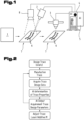
- the method for fabricating at least one conductive circuit structure layer 6, for instance a trace or at least a longitudinal section of a trace, on or in a component carrier 7, for instance a printed circuit board, and with at least one specific electric or electronic property, as in its essential steps shown in the block diagram of Fig. 2 comprises the step of manufacturing a conductive structure layer 6 or changing or reworking a prefabricated conductive structure layer 6.
- Such structure layers are produced based on models combining design parameters with desired electric or electronic properties, in particular the impedance.
- the next step in the process according to the invention is to acquire - preferably by measurement or detection method(s) or any kind of equivalent input - actual data from at least one conductive structure layer of a component carrier (see as an exemplary embodiment an imaging device 8, such as a camera, in Fig. 1 ).
- This can be done in particular comprising capturing one or more images of the structure layer.
- the capturing of at least one image of the structure layer may be done preferably using light in the visible range and/or using X-ray radiation, allowing to detect in the visible light range exposed structures and/or in the X-ray range non-exposed/embedded structures. Even other spectral bands may be used for special purposes.
- the structure layer measurement can be done also by direct and/or indirect measurement also through physical tools like pointers or by optical tools, preferably using the IR-range. Further, electric values measurement, e.g. a two-four wires test, or a ground measurement could be provided for data acquisition in this early stage.
- said (acquired) actual data of said at least one conductive structure layer are fed into at least one model, said model determining - in dependence of said actual data of said at least one conductive structure layer and in dependence of at least one predefined electric or electronic property for the conductive structure layer - at least one adjusted design parameter for the conductive structure layer, allowing to preferably establish a PE/CAM (Process Engineering/Computer Aided Manufacturing) system.
- the at least one adjusted design parameter may relate to a geometric characteristic and/or a material characteristic of the conductive structure layer, in particular the structure layer width, the structure layer thickness, the structure layer length, the structure layer roughness, the structure layer porosity and/or the structure layer material.
- the step of manufacturing a conductive structure layer or changing or reworking a pre-fabricated conductive structure layer is performed in a dynamic production environment.
- a dynamic production environment with at least one feedback loop, into which loop the data acquired from and about the structure layer are fed back.
- a feedback loop into an AI based software environment and adjusting at least one parameter guided by AI based software based on said feedback loop.
- the main feature to take into consideration is the data-based model being trained by any suitable algorithm (e.g. by a machine learning method such as artificial (deep) neuronal net, Bayesian Algorithms, Clustering Algorithms etc.) in order to rank the feedbacks and the eventual variables to adapt the subsequent performances evaluation/calculation/modification.
- most relevant parameters that can be processed by the AI system are at least one of the group of the (plating) thickness, the structure layer pattern design parameters, the structure layer surface (roughness, porosity) or the material treatment.
- the manufacturing, adjustment or reworking of the structure layer is then performed with at least one adjusted process design parameter loaded after the AI system has processed the acquired data and relating them to the desired properties of the structure layer. That means that said process design parameter is based on at least one output from said at least one feedback loop and is implemented in the fabricating process of the at least one conductive structure layer.
Landscapes
- Engineering & Computer Science (AREA)
- Microelectronics & Electronic Packaging (AREA)
- Physics & Mathematics (AREA)
- Manufacturing & Machinery (AREA)
- Theoretical Computer Science (AREA)
- General Health & Medical Sciences (AREA)
- General Physics & Mathematics (AREA)
- Computational Linguistics (AREA)
- Data Mining & Analysis (AREA)
- Evolutionary Computation (AREA)
- Biomedical Technology (AREA)
- Molecular Biology (AREA)
- Computing Systems (AREA)
- General Engineering & Computer Science (AREA)
- Biophysics (AREA)
- Mathematical Physics (AREA)
- Software Systems (AREA)
- Artificial Intelligence (AREA)
- Life Sciences & Earth Sciences (AREA)
- Computer Hardware Design (AREA)
- Health & Medical Sciences (AREA)
- Manufacturing Of Printed Wiring (AREA)
Priority Applications (2)
| Application Number | Priority Date | Filing Date | Title |
|---|---|---|---|
| EP23198894.0A EP4529369A1 (de) | 2023-09-21 | 2023-09-21 | Verfahren zur herstellung von mindestens einer leitfähigen strukturschicht auf oder in einem komponententräger |
| PCT/EP2024/076184 WO2025061808A1 (en) | 2023-09-21 | 2024-09-19 | A method for fabricating at least one conductive structure layer on or in a component carrier |
Applications Claiming Priority (1)
| Application Number | Priority Date | Filing Date | Title |
|---|---|---|---|
| EP23198894.0A EP4529369A1 (de) | 2023-09-21 | 2023-09-21 | Verfahren zur herstellung von mindestens einer leitfähigen strukturschicht auf oder in einem komponententräger |
Publications (1)
| Publication Number | Publication Date |
|---|---|
| EP4529369A1 true EP4529369A1 (de) | 2025-03-26 |
Family
ID=88147135
Family Applications (1)
| Application Number | Title | Priority Date | Filing Date |
|---|---|---|---|
| EP23198894.0A Withdrawn EP4529369A1 (de) | 2023-09-21 | 2023-09-21 | Verfahren zur herstellung von mindestens einer leitfähigen strukturschicht auf oder in einem komponententräger |
Country Status (2)
| Country | Link |
|---|---|
| EP (1) | EP4529369A1 (de) |
| WO (1) | WO2025061808A1 (de) |
Citations (5)
| Publication number | Priority date | Publication date | Assignee | Title |
|---|---|---|---|---|
| US20030088802A1 (en) | 1999-08-27 | 2003-05-08 | David Cuthbert | Method and apparatus for reducing signal timing skew on a printed circuit board |
| US20050168318A1 (en) * | 2002-11-21 | 2005-08-04 | Nicholas Biunno | Laser trimming of resistors |
| KR20070085202A (ko) | 2004-06-28 | 2007-08-27 | 에스브이 프로브 피티이 엘티디 | 패턴화된 도전층을 구비한 기판 |
| KR102203169B1 (ko) * | 2019-12-30 | 2021-01-14 | 주식회사 태크녹스 | 저항성 온도센서의 교정장치 |
| CN216565769U (zh) | 2021-10-01 | 2022-05-17 | 联策科技股份有限公司 | 智慧化电路板蚀刻装置 |
-
2023
- 2023-09-21 EP EP23198894.0A patent/EP4529369A1/de not_active Withdrawn
-
2024
- 2024-09-19 WO PCT/EP2024/076184 patent/WO2025061808A1/en active Pending
Patent Citations (5)
| Publication number | Priority date | Publication date | Assignee | Title |
|---|---|---|---|---|
| US20030088802A1 (en) | 1999-08-27 | 2003-05-08 | David Cuthbert | Method and apparatus for reducing signal timing skew on a printed circuit board |
| US20050168318A1 (en) * | 2002-11-21 | 2005-08-04 | Nicholas Biunno | Laser trimming of resistors |
| KR20070085202A (ko) | 2004-06-28 | 2007-08-27 | 에스브이 프로브 피티이 엘티디 | 패턴화된 도전층을 구비한 기판 |
| KR102203169B1 (ko) * | 2019-12-30 | 2021-01-14 | 주식회사 태크녹스 | 저항성 온도센서의 교정장치 |
| CN216565769U (zh) | 2021-10-01 | 2022-05-17 | 联策科技股份有限公司 | 智慧化电路板蚀刻装置 |
Also Published As
| Publication number | Publication date |
|---|---|
| WO2025061808A1 (en) | 2025-03-27 |
Similar Documents
| Publication | Publication Date | Title |
|---|---|---|
| EP3878826A1 (de) | Komponententräger und verfahren zur herstellung davon | |
| CN111511105B (zh) | 具有用额外镀覆结构和桥结构填充的通孔的部件承载件 | |
| US8215011B2 (en) | Method of manufacturing a printed circuit board | |
| CN210928127U (zh) | 部件承载件 | |
| CN111511102B (zh) | 在通孔中具有符合最小距离设计原则的桥结构的部件承载件 | |
| WO2006089255A2 (en) | High aspect ratio plated through holes in a printed circuit board | |
| US12117810B2 (en) | AI-based determination of action plan for manufacturing component carriers | |
| CN105744739B (zh) | 印刷电路板及其制造方法 | |
| US11166385B2 (en) | Component carrier having a laser via and method of manufacturing | |
| CN102523703A (zh) | 一种pcb板上背钻孔的制作方法 | |
| US20220095457A1 (en) | Component Carrier With Blind Hole Filled With An Electrically Conductive Medium And Fulfilling A Minimum Thickness Design Rule | |
| TWI407869B (zh) | 製造電路化基板之方法 | |
| EP4529369A1 (de) | Verfahren zur herstellung von mindestens einer leitfähigen strukturschicht auf oder in einem komponententräger | |
| WO2024062396A1 (en) | A galvanic plating apparatus and a method for galvanically plating a component carrier structure | |
| CN112087887A (zh) | 通过组合评估垫型和孔型对准标记来对准部件承载件结构 | |
| US6846993B2 (en) | Multilayer printed wiring board and its manufacturing method | |
| US11439026B2 (en) | Printed circuit board | |
| KR102793570B1 (ko) | 부품 캐리어 제조용 패널의 열-유도 및 압력-유도 적층을 위한 열 관리 | |
| US11284511B2 (en) | Component carrier with different surface finishes and method for manufacturing the same | |
| Bupp et al. | High-density board fabrication techniques | |
| JP2015220354A (ja) | 配線基板の製造方法 | |
| JP2003008238A (ja) | 多層プリント板用穴明け加工機及びそれを用いた製造方法。 | |
| CN113316324B (zh) | 一种hdi板制造工艺 | |
| CN118250937B (zh) | 一种任意层互连印刷线路板制作工艺 | |
| JP2001230508A (ja) | ストリップライン構造のバイアホールおよびその製造方法 |
Legal Events
| Date | Code | Title | Description |
|---|---|---|---|
| PUAI | Public reference made under article 153(3) epc to a published international application that has entered the european phase |
Free format text: ORIGINAL CODE: 0009012 |
|
| STAA | Information on the status of an ep patent application or granted ep patent |
Free format text: STATUS: THE APPLICATION HAS BEEN PUBLISHED |
|
| AK | Designated contracting states |
Kind code of ref document: A1 Designated state(s): AL AT BE BG CH CY CZ DE DK EE ES FI FR GB GR HR HU IE IS IT LI LT LU LV MC ME MK MT NL NO PL PT RO RS SE SI SK SM TR |
|
| STAA | Information on the status of an ep patent application or granted ep patent |
Free format text: STATUS: THE APPLICATION IS DEEMED TO BE WITHDRAWN |
|
| 18D | Application deemed to be withdrawn |
Effective date: 20250927 |