JP2004014207A - Semiconductor circuit pattern inspection equipment - Google Patents
Semiconductor circuit pattern inspection equipment Download PDFInfo
- Publication number
- JP2004014207A JP2004014207A JP2002163701A JP2002163701A JP2004014207A JP 2004014207 A JP2004014207 A JP 2004014207A JP 2002163701 A JP2002163701 A JP 2002163701A JP 2002163701 A JP2002163701 A JP 2002163701A JP 2004014207 A JP2004014207 A JP 2004014207A
- Authority
- JP
- Japan
- Prior art keywords
- electron beam
- circuit pattern
- center
- electron
- semiconductor circuit
- Prior art date
- Legal status (The legal status is an assumption and is not a legal conclusion. Google has not performed a legal analysis and makes no representation as to the accuracy of the status listed.)
- Granted
Links
Images


Landscapes
- Testing Or Measuring Of Semiconductors Or The Like (AREA)
- Electron Sources, Ion Sources (AREA)
Abstract
【課題】半導体装置の製造過程にあるウェハ上の半導体装置の回路パターンの欠陥を電位コントラストにより検出する装置において、電子源を複数備えることなく高感度に検出可能とする。
【解決手段】電子線の電流を制限する絞りに、光軸中心の孔以外の孔を周囲に1個または複数個設け、それらの孔を通過した電子線が対物レンズの球面収差の作用により中心の孔からの電子線の着地点よりやや離れた場所に着地するようにする。
【選択図】図1An apparatus for detecting a defect in a circuit pattern of a semiconductor device on a wafer in a process of manufacturing the semiconductor device by using a potential contrast can be detected with high sensitivity without providing a plurality of electron sources.
One or more holes other than the hole at the center of the optical axis are provided around a stop for limiting the current of the electron beam, and the electron beam passing through those holes is centered by the action of the spherical aberration of the objective lens. So that it lands slightly away from the point where the electron beam lands through the hole.
[Selection diagram] Fig. 1
Description
【0001】
【発明の属する技術分野】
本発明は半導体装置製造過程のウェハ上の回路パターンの検査に好適な電子線応用装置に関する。
【0002】
【従来の技術】
半導体装置の製造過程において、ウェハ上に形成された回路パターンの欠陥を比較検査して検出する検査方法には、例えば1つのウェハ上の2つ以上のLSIの同種パターンの画像をSEMにより取得し、それらを比較し、あらかじめ設定した閾値よりも明るさに差がある部分を回路パターンの欠陥として表示する欠陥検査装置が実用化されている。それら従来技術は、例として特開昭59−192943号公報、特開平5−258703号公報、文献J.Vac.Sci.Tech.B,Vol.9,No.6,pp.3005−3009(1991)、J.Vac.Sci.Tech.B,Vol.10,No.6,pp.2511−2515(1992),SPIEVol.2439,等に記載されている。
【0003】
上記従来技術においては、実用的なスループットを得るために、非常に高速に画像を取得する必要がある。そして高速で取得した画像のSNを確保するために通常の走査型電子顕微鏡の100倍以上(10nA以上)の電子線電流を用い、実用的な検査速度を維持しながら画像のSNを確保している。
【0004】
また、上述のような電子線を用いた検査装置では、絶縁されているものは帯電が発生するので、光では検出できない欠陥、すなわち電気的欠陥が検出できるのがひとつの特徴である。電気的欠陥とは、導通すべき部分が電気的に絶縁されていたり、逆に絶縁されているべき箇所がショートしていたりする欠陥である。
【0005】
特開平10−294345には、特に絶縁物を含む回路パターンや電気的欠陥を高感度に再現性よく検査するために、ウェハ上の回路パターンを所望の電位に積極的に帯電させる手段について記述されている。これによると、大電流の電子ビームを一回のみ走査させて画像を取得することや、高分解能な検査画像を形成するために、電子ビームの主発生源以外に1個または複数個の電子源を備え、それらの電子源からの電子ビームのエネルギや照射量を制御してウェハ回路パターンに照射することで、所望の帯電電位に設定することが可能となると記されている。
【0006】
また、電子ビームによるウェハ回路パターン検査によれば、回路パターンに設けられた層間の導通用の孔の非導通欠陥を電位コントラストにより高感度に検査できる。この技術に関しては、特開2000−208579号公報等に記載されている。ここではウェハをあらかじめ所望の電位に帯電させるために画像形成に用いる電子ビームとは別個の電子源(フラッドガン)を設けている。
【0007】
【発明が解決しようとする課題】
上記した、電子線により絶縁物を含むウェハ回路パターンの欠陥を安定にかつ高感度に検査するために、大電流の一回走査で画像を取得することが記されているが、回路パターンの電気的特性によっては、あらかじめ帯電させておかないと十分なコントラストが得られないものがあった。これを解決するには、複数の電子源を設ける必要があることが述べられている。
【0008】
しかし、複数の電子源を設けることはそれだけ電子ビームの制御が困難となり装置も大型化する。また2つ以上の電子ビームを最適な条件でウェハ上の所望の領域に照射するためには制御系が電子源の数だけ必要となり装置価格の増加や調整の長時間化等問題が多かった。
【0009】
本発明の課題は、従来の大電流一回走査では十分なコントラストが得られなかった半導体回路パターンにおいても複数の電子源を備えることなく画像形成用の電子源のみで、高速、安定かつ明暗コントラストの大きい良質の画像として取得し、その画像を自動比較検査し欠陥を誤りなく検出することである。
【0010】
【課題を解決するための手段】
電子線を発生する電子源と電子線を被検査半導体回路パターン上に集束する対物レンズと上記電子線の電流量を調整するための絞りと電子線を被検査半導体回路パターンの所望の位置に位置付けるための偏向器と絶縁物を含む上記被検査半導体回路パターンの第1と第2の領域の画像を電子線により取得した画像を比較することで上記被検査半導体回路パターンの欠陥を検査する装置において、上記絞りに、電子線の光軸中心にほぼ一致する位置に備えた中心孔と、中心孔の周囲に中心穴と比較して小さい孔を1個または複数個設ける。上記絞りの中心孔の中心と周囲の小さい孔の中心の距離は、周囲の小さい孔を通過した電子線が対物レンズ中心軸の十分外側を通過し、中心孔を通過した電子線が半導体回路パターン上に焦点を結ぶ場所よりも離れた位置に照射されるようにすることで課題を解決できる。
【0011】
【発明の実施の形態】
まず、本発明がなされるきっかけとなった現象について説明し、本発明の動作原理を説明する。
【0012】
電子ビームを用いて絶縁膜を含む半導体を観察するとき、絶縁膜表面は電子ビームの照射エネルギや表面の電界に応じた電荷を帯びる。通常、プラスに帯電したところは暗く、マイナスに帯電したところは明るいコントラストが生じる。これを電位コントラストと呼んでいる。
【0013】
SEMを応用したウェハ検査装置では、前記したように検査時間短縮のために大電流(100nA程度)の電子ビームを高速に一回だけ走査することで画像を形成している。このとき、電子ビームの焦点が外れた状態、すなわち径の大きな電子ビームでSEM画像を形成すると導電物と絶縁物の回路パターンの明るさの違いすなわちコントラストが強調されるという現象がしばしば発生した。コントラストが強調されることで微小な形状欠陥や導通不良欠陥が感度よく検出できることが期待される。
【0014】
この原因は以下のように考えられる。導電物と絶縁物が混在する回路パターンでは、絶縁物が電子ビームの照射により帯電し、導電物がグランド電位を維持することで電位コントラストが発生する。小さい直径の電子ビームを走査する場合、絶縁物が十分帯電しきらない短い時間で電子ビームが隣の位置に移動してしまうため、画像形成時すなわち二次電子が発生したときの絶縁物の帯電電位は低い。一方、電子ビームの直径が大きい場合は、電子ビームが同一箇所を比較的長い時間照射することとなり、画像形成時の絶縁物の帯電電位は比較的高い。これがフォーカスをずらして電子ビームの直径を大きくした場合にコントラストが強調される原因と考えられる。
【0015】
同様の原理で、あらかじめ電子ビームを照射しておき、十分に帯電させてから観察すれば、同様にコントラストの強い画像が得られるはずである。ところが、多数のウェハにおいて観察、または検査前に電子ビームを照射したのでは十分なコントラストが得られないという現象が発生した。これは、一度帯電しても時間が経過することで電荷が逃げてしまうためと考えられる。この電荷の逃げる時間はデバイスの構造や絶縁膜の種類によって決まると考えられる。
【0016】
したがって、デフォーカスによるコントラスト強調が最も効果があることがわかる。しかし、フォーカスをずらした状態では半導体の微細な回路パターンを分離して高分解能に観察することが不可能になる。
【0017】
本発明においては、中心部では直径の小さい鋭いピークを持ち、周辺部にはある程度広がった分布を持ちながら電流密度が小さく、中心のピークに含まれる電荷量と比較して、周辺部の電荷量が十分少ない分布を持った電子ビームを形成することで、上記の問題を解決した。
【0018】
以下では、上記のような特徴を持った電子ビームを形成し、回路パターンを検査する装置の構成例を、図面を参照しながら詳細に説明する。
(実施例1)
本発明の基本概念は、穴を複数個備えた電流制限絞りを用いることで実現する。以下、図1に第1の実施例の構成図を示す。本実施例の検査装置は大別して電子光学系101、試料室102、制御部104、画像処理部105より構成されている。
【0019】
電子光学系101は電子銃1、電子線引き出し電極2、コンデンサレンズ3、ブランキング用偏向器4、走査偏向器5、絞り6、対物レンズ7により構成されている。
【0020】
試料室102は、X−Yステージ8、回転ステージ9、位置モニタ用測長器10、被検査基板高さ測定器11より構成されており、また二次電子検出器12が対物レンズ7の上方にあり、二次電子検出器12の出力信号はプリアンプ13で増幅されAD変換器14によりデジタルデータとなる。
【0021】
画像処理部105は画像記憶部18・19、演算部20、欠陥判定部21より構成されている。取り込まれた電子線画像および光学画像は、モニタ22に表示される。
【0022】
検査装置各部の動作命令および動作条件は、制御部104から入出力される。あらかじめ制御部104に電子線発生時の加速電圧・電子線偏向幅・偏向速度・試料台移動速度・検出器の信号取り込みタイミング等々の条件が入力されている。また、位置モニタ用測長器10、被検査基板高さ測定器11の信号から補正信号を生成し、電子線が常に正しい位置に照射されるように、対物レンズ電源26や走査信号発生器28に補正信号を送る。
【0023】
本実施例において、電子銃1には拡散補給型の熱電界放出電子源を用いた。これにより明るさ変動の少ない比較検査画像が得られ、かつ電子ビーム電流を大きくすることが可能で、高速検査が可能になる。電子線は引出電極2に電圧を印加することで電子銃1から引き出される。電子線の加速は電子銃1に高圧の負の電位を印加することでなされ、電子線はその電位に相当するエネルギで試料台8の方向に進み、コンデンサレンズ3で収束され、絞り6により通過する電流量が制限される。
【0024】
図2に、上記絞り6の穴の構造の一例を示す。絞り6は、その中心に直径30〜50μm程度の中心孔61、中心孔61の周辺には10μm以下の直径の周辺孔62が1個ないし6個程度設けられている(図2では周辺孔62が4個の場合を示した)。この絞り6の孔61もしくは62を通過した電子ビームは、対物レンズ47により細く絞られ、X−Yステージ8の上に搭載された被検査基板23(ウェハあるいはチップ等)に照射される。
【0025】
被検査基板23には高圧電源25により負の電圧を印加できるようになっている。この高圧電源25を調節することにより被検査基板23への電子線照射エネルギを最適な値に調節することが容易となる。画像形成には、XYステージ8を静止させ電子線201を二次元に走査する方法と、電子線は一次元走査し走査方向と直行する方向にXYステージ8を連続的に移動する方法のいずれかを選択できる。ある特定の場所を検査する場合にはステージを静止させて検査し、被検査基板23の広い範囲を検査するときはステージを連続移動して検査すると効率のよい検査が行える。
【0026】
試料室102に被検査基板23が移動すると、電子銃1からの電子線201で比較検査用の画像を取得して比較検査を実行する。被検査基板23の画像を取得するためには、細く絞った電子線201を上記被検査基板23に照射し、二次電子および反射電子を発生させ、これらを電子線201の走査およびステージの移動と同期して検出することで被検査基板表面の画像を得る。
【0027】
本発明で述べるような自動検査では、検査速度が速いことが必須となる。したがって通常のSEMのようにpAオーダのビーム電流を低速で走査したり、複数回走査は行わない。そこで、通常のSEMに比べ約100倍以上の、例えば100nAの大電流電子線を一回だけ走査することにより画像を形成する構成とした。一枚の画像は1000×1000画素で、これを約10msecで取得するようにした。
【0028】
上記構成において、絞り6の中心孔61と周辺孔62により被検査基板23上の電子線の形状がどのようなものになるかを説明する。中心孔61の半径をR1、中心孔61を通過した電子線36の被検査基板23上の照射角をα1とする。また、周辺孔62の中心孔61の中心からの距離をR2とし、周辺孔62を通過した電子線37の光軸中心からの角度をα2とする。なお、被検査基板23には高圧電源25により負の電位が印加されており、電子線36、37は基板23直前で減速されるため実際の照射角は基板23直前で数倍に増大する。ここでは説明を簡単にするために、高圧電源25がゼロ電位の場合について説明する。なお、負電位が印加されている場合は照射角等の値が一定の割合で拡大するだけである。
【0029】
中心孔61を通過した電子線36はほぼ100nAの電流で被検査基板23上の直径はおよそ0.1μmまたはそれ以下になっている。この直径は、対物レンズ7とコンデンサレンズ3の球面収差と色収差およびビームの照射角で決まる回折収差、さらには空間電荷効果と電子源の光源の大きさで決定される。これらの収差のうち球面収差と色収差は絞り半径R1が大きいほど増大し、回折収差と空間電荷効果は小さいほど増大する。中心孔61の半径R1は、電子線36が所定のビーム電流(例えば100nA)において、これらの収差が最小となるような条件に最適化されている。例えば15〜25μm程度である。
【0030】
一方、周辺孔62の中心からの距離R2は収差の最適値R1より非常に大きい。したがって周辺孔62を通過した電子線37は対物レンズ7の中心から大きく離れた角度を通過するために球面収差と色収差が大きくなる。特に球面収差は照射角の3乗に比例するために急激に大きくなる。球面収差とはレンズの中心軸から離れた軌道を通る電子線ほど焦点が短くなる収差と定義される。
【0031】
これらの電子線の概念図を図3(a)と図3(b)に示す。図3(a)は絞り6と対物レンズ7を含んだ図で、周辺孔62を通過した電子線37は中心孔61を通過した電子線36よりも手前に焦点を結んでいる。図3(b)は、被検査基板23の近傍を拡大した図で、電子線37は電子線36の周辺部を広がって照射することになる。
【0032】
図3(c)は被検査基板23上に照射される電子の断面密度分布を示したものである。中心は鋭く立ちあがったピークを持ち、その周辺に小さなピークを持つことになる。ピークに含まれる電流は100nA程度であり、周辺部のなだらかな分布に含まれる電流は、周辺孔62の大きさを十分小さくすることにより1nA以下に小さくすることができる。なお、周辺孔62を通過した電子線37の位置が中心の電子線36に対して、電子線の走査方向に存在するように周辺孔62が配置されている。
【0033】
以下、一例として具体的な数値を示す。対物レンズ7の球面収差係数をCsとし、中心孔61を通過した電子線36の被検査基板上の直径をd1、電子線37の光軸中心からの距離の2倍をd2、ビーム直径をDdとする。これらの関係は以下の式により表すことができる。
【0034】
【数1】
【0035】
以上説明してきた構成により、絶縁物を含む半導体回路パターンを観察した例を説明する。
【0036】
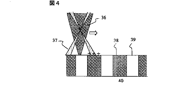
図4はSi基板40上に酸化膜38と導通孔39が形成されている構造を模式的に示したものである。ここでは導通孔39にはタングステンが埋め込まれている場合について説明する。中心部の鋭いピークを持った大電流の電子線36と、その周囲の電子線37が左から右に走査されている。電子線37が酸化膜38をあらかじめ帯電させた後に電子線36が照射されるため、このとき酸化膜38がプラスに帯電された状態で二次電子が発生する。このため、この電界の作用を受け、試料の電位コントラストが明確に観察される。
【0037】
このときの画像は、例えば図5のように酸化膜部分は十分に暗く、導通孔部分は十分に明るい像となる。仮に、非導通の欠陥孔があれば、その部分だけ酸化膜と同様に暗くなるために、すぐに欠陥として検出することが可能であった。
【0038】
一方、図6は、中心部の電子線36のみで観察した従来の構成での観察例である。電子線36が照射されるまで電子線の照射を受けていないため、帯電が十分進まないうちに電子線36が通過して画像を形成してしまう。したがって、酸化膜部と導通孔部の明るさにほとんど違いが認められず、仮に導通していない孔が存在しても検出することが困難であった。
【0039】
【発明の効果】
本発明によれば、半導体の回路パターンの欠陥、異物、残渣等を電子線走査で検査する方法において、レジストパターンや酸化膜等の非導電性の表面を持った半導体ウェハの検査が可能となった。
【0040】
これにより、製造過程で発生した従来装置で検出できない欠陥を発見可能にし、半導体プロセスにフィードバックすることにより、半導体装置の不良率を低減し、信頼性を向上した。
【図面の簡単な説明】
【図1】本発明の一実施例の半導体回路パターン検査装置の全体構成を示す図。
【図2】本発明の一実施例の電子線絞りの平面図。
【図3】本発明の原理および本発明による電子線の強度分布を示す図。
【図4】本発明の動作状態の説明図。
【図5】本発明の一実施例により取得した画像を示す図。
【図6】従来の装置で取得した画像を示す図。
【符号の説明】
1…電子銃、2引き出し電極、3…コンデンサレンズ、4…ブランキング用偏向器、5…走査偏向器、6…絞り、7…対物レンズ、8…X−Yステージ、9…回転ステージ、10…位置モニタ用測長器、11…光学式試料高さ測定器、12…二次電子検出器、13…プリアンプ、14…AD変換器、18…画像記憶部、19…画像記憶部、20…演算部、21…欠陥判定部、22…モニタ、23…被検査基板、24…ステージ、25…高圧電源、26…対物レンズ電源、27…補正制御回路、28…走査信号発生器、36…中心部の電子線、37…周辺部の電子線、61…中心孔、62…周辺孔、101…電子光学系、102…試料室、103…予備室、104…制御部、105…画像処理部。[0001]
TECHNICAL FIELD OF THE INVENTION
The present invention relates to an electron beam application apparatus suitable for inspecting a circuit pattern on a wafer in a semiconductor device manufacturing process.
[0002]
[Prior art]
In an inspection method of comparing and detecting a defect of a circuit pattern formed on a wafer in a manufacturing process of a semiconductor device, an image of a similar pattern of two or more LSIs on one wafer is acquired by SEM, for example. A defect inspection apparatus has been put to practical use that compares them and displays a portion having a difference in brightness from a preset threshold value as a defect in a circuit pattern. These prior arts are described in, for example, JP-A-59-192943, JP-A-5-258703, and J. J. Vac. Sci. Tech. B, Vol. 9, No. 6, pp. 3005-3009 (1991); Vac. Sci. Tech. B, Vol. 10, No. 6, pp. 2511-2515 (1992), SPIEVol. 2439, etc.
[0003]
In the above prior art, it is necessary to acquire an image at a very high speed in order to obtain a practical throughput. Then, in order to secure the SN of the image acquired at high speed, an electron beam current of 100 times or more (10 nA or more) of the ordinary scanning electron microscope is used, and the SN of the image is secured while maintaining a practical inspection speed. I have.
[0004]
One of the features of the inspection apparatus using an electron beam as described above is that a defect that cannot be detected by light, that is, an electrical defect can be detected because an insulated object is charged. An electrical defect is a defect in which a portion to be conducted is electrically insulated or a portion to be insulated is short-circuited.
[0005]
Japanese Patent Application Laid-Open No. H10-294345 describes a means for positively charging a circuit pattern on a wafer to a desired potential in order to inspect a circuit pattern including an insulator and an electrical defect with high sensitivity and high reproducibility. ing. According to this, in order to acquire an image by scanning a large current electron beam only once and to form a high-resolution inspection image, one or more electron sources other than the main source of the electron beam are used. It is described that by controlling the energy and the irradiation amount of the electron beam from these electron sources and irradiating the wafer circuit pattern, a desired charging potential can be set.
[0006]
Further, according to the wafer circuit pattern inspection using an electron beam, a non-conduction defect of a conduction hole between layers provided in a circuit pattern can be inspected with high sensitivity by a potential contrast. This technique is described in JP-A-2000-208579 and the like. Here, an electron source (flood gun) separate from the electron beam used for image formation is provided in order to previously charge the wafer to a desired potential.
[0007]
[Problems to be solved by the invention]
As described above, in order to stably and highly sensitively inspect a defect of a wafer circuit pattern including an insulator by an electron beam, an image is acquired by a single scan of a large current. In some cases, a sufficient contrast cannot be obtained unless charged beforehand. It is stated that in order to solve this, it is necessary to provide a plurality of electron sources.
[0008]
However, providing a plurality of electron sources makes it more difficult to control the electron beam, which also increases the size of the apparatus. Further, in order to irradiate a desired area on a wafer with two or more electron beams under optimum conditions, a control system is required for the number of electron sources, and there are many problems such as an increase in apparatus price and a long adjustment time.
[0009]
It is an object of the present invention to provide a high-speed, stable and bright / dark contrast using only an electron source for forming an image without providing a plurality of electron sources even in a semiconductor circuit pattern in which sufficient contrast cannot be obtained by a conventional large current single scan. Is to obtain a high-quality image having a large size, automatically compare and inspect the image, and detect a defect without error.
[0010]
[Means for Solving the Problems]
An electron source for generating an electron beam, an objective lens for focusing the electron beam on the semiconductor circuit pattern to be inspected, an aperture for adjusting the amount of current of the electron beam, and the electron beam being positioned at a desired position on the semiconductor circuit pattern to be inspected An apparatus for inspecting a defect of the semiconductor circuit pattern to be inspected by comparing images of the first and second regions of the semiconductor circuit pattern to be inspected including the deflector and the insulator by an electron beam. The diaphragm is provided with a center hole provided at a position substantially coincident with the center of the optical axis of the electron beam, and one or more holes around the center hole which are smaller than the center hole. The distance between the center of the center hole of the aperture and the center of the surrounding small hole is such that the electron beam passing through the small surrounding hole passes sufficiently outside the center axis of the objective lens, and the electron beam passing through the center hole is the semiconductor circuit pattern. The problem can be solved by irradiating the light at a position distant from the place where the focal point is focused upward.
[0011]
BEST MODE FOR CARRYING OUT THE INVENTION
First, the phenomenon that triggered the present invention will be described, and the operation principle of the present invention will be described.
[0012]
When observing a semiconductor including an insulating film with an electron beam, the surface of the insulating film is charged with energy corresponding to the irradiation energy of the electron beam or the electric field on the surface. Normally, a positively charged area produces a dark contrast, and a negatively charged area produces a bright contrast. This is called a potential contrast.
[0013]
In the wafer inspection apparatus to which the SEM is applied, as described above, an image is formed by scanning once with a high-current (about 100 nA) electron beam at a high speed in order to shorten the inspection time. At this time, when the SEM image is formed in a state where the electron beam is out of focus, that is, when an electron beam having a large diameter is formed, a phenomenon often occurs in which a difference in brightness, that is, a contrast between circuit patterns of a conductor and an insulator is emphasized. By enhancing the contrast, it is expected that minute shape defects and conduction defect can be detected with high sensitivity.
[0014]
The cause is considered as follows. In a circuit pattern in which a conductor and an insulator are mixed, the insulator is charged by irradiation of an electron beam, and a potential contrast is generated by maintaining the ground potential of the conductor. When scanning an electron beam with a small diameter, the electron beam moves to the next position in a short time when the insulator is not sufficiently charged, so that the insulator is charged during image formation, that is, when secondary electrons are generated. The potential is low. On the other hand, when the diameter of the electron beam is large, the same portion is irradiated with the electron beam for a relatively long time, and the charged potential of the insulator during image formation is relatively high. This is considered to be the cause of enhancing the contrast when the diameter of the electron beam is increased by shifting the focus.
[0015]
According to the same principle, if an electron beam is irradiated in advance and sufficiently charged, and observed, an image having a similarly high contrast should be obtained. However, a phenomenon has occurred in which a sufficient contrast cannot be obtained by irradiating an electron beam on a large number of wafers before observation or inspection. It is considered that this is because the charge escapes over time even if it is charged once. It is considered that the time for the charge to escape depends on the structure of the device and the type of the insulating film.
[0016]
Therefore, it is understood that contrast enhancement by defocus is most effective. However, in a state where the focus is shifted, it becomes impossible to separate a fine circuit pattern of a semiconductor and observe it at a high resolution.
[0017]
In the present invention, the central portion has a sharp peak with a small diameter, the peripheral portion has a somewhat wide distribution, and the current density is small, and the charge amount in the peripheral portion is smaller than that in the central peak. The above problem was solved by forming an electron beam having a sufficiently small distribution.
[0018]
Hereinafter, a configuration example of an apparatus that forms an electron beam having the above characteristics and inspects a circuit pattern will be described in detail with reference to the drawings.
(Example 1)
The basic concept of the present invention is realized by using a current limiting aperture having a plurality of holes. FIG. 1 shows a configuration diagram of the first embodiment. The inspection apparatus of the present embodiment is roughly composed of an electron
[0019]
The electron
[0020]
The
[0021]
The
[0022]
Operation commands and operation conditions of each part of the inspection apparatus are input and output from the
[0023]
In this embodiment, a diffusion-supply type thermal field emission electron source was used for the electron gun 1. As a result, it is possible to obtain a comparative inspection image with a small variation in brightness, increase the electron beam current, and perform high-speed inspection. The electron beam is extracted from the electron gun 1 by applying a voltage to the
[0024]
FIG. 2 shows an example of the structure of the hole of the stop 6. The aperture 6 is provided with a central hole 61 having a diameter of about 30 to 50 μm at the center thereof and one to six peripheral holes 62 having a diameter of 10 μm or less around the central hole 61 (the peripheral hole 62 in FIG. 2). Is four). The electron beam that has passed through the holes 61 or 62 of the aperture 6 is narrowed down by the objective lens 47 and irradiates the substrate 23 (eg, wafer or chip) mounted on the XY stage 8.
[0025]
A negative voltage can be applied to the
[0026]
When the substrate to be inspected 23 moves to the
[0027]
In the automatic inspection as described in the present invention, a high inspection speed is essential. Therefore, unlike a normal SEM, a beam current of the order of pA is scanned at a low speed, and scanning is not performed a plurality of times. Therefore, an image is formed by scanning only once with a high-current electron beam of, for example, 100 nA, which is about 100 times or more that of a normal SEM. One image is 1000 × 1000 pixels, which are acquired in about 10 msec.
[0028]
In the above configuration, the shape of the electron beam on the
[0029]
The
[0030]
On the other hand, the distance R 2 from the center of the peripheral hole 62 is much larger than the optimum value R 1 of the aberration. Therefore, since the
[0031]
FIGS. 3A and 3B are conceptual diagrams of these electron beams. FIG. 3A is a view including the diaphragm 6 and the objective lens 7. The
[0032]
FIG. 3C shows a cross-sectional density distribution of electrons irradiated onto the
[0033]
Hereinafter, specific numerical values are shown as an example. The spherical aberration coefficient of the objective lens 7 is Cs, the diameter of the
[0034]
(Equation 1)
[0035]
An example in which a semiconductor circuit pattern including an insulator is observed with the configuration described above will be described.
[0036]
FIG. 4 schematically shows a structure in which an
[0037]
The image at this time is, for example, as shown in FIG. 5, the oxide film portion is sufficiently dark and the conduction hole portion is sufficiently bright. If there is a non-conductive defect hole, only that portion becomes dark like the oxide film, so that it can be immediately detected as a defect.
[0038]
On the other hand, FIG. 6 shows an example of observation with a conventional configuration in which observation was made only with the
[0039]
【The invention's effect】
According to the present invention, it is possible to inspect a semiconductor wafer having a non-conductive surface such as a resist pattern or an oxide film in a method of inspecting a semiconductor circuit pattern for defects, foreign matter, residues, and the like by electron beam scanning. Was.
[0040]
This makes it possible to discover defects that cannot be detected by the conventional device during the manufacturing process, and feeds back to the semiconductor process, thereby reducing the defect rate of the semiconductor device and improving the reliability.
[Brief description of the drawings]
FIG. 1 is a diagram showing an overall configuration of a semiconductor circuit pattern inspection apparatus according to one embodiment of the present invention.
FIG. 2 is a plan view of an electron beam stop according to one embodiment of the present invention.
FIG. 3 is a diagram showing the principle of the present invention and the intensity distribution of an electron beam according to the present invention.
FIG. 4 is an explanatory diagram of an operation state of the present invention.
FIG. 5 is a diagram showing an image acquired according to an embodiment of the present invention.
FIG. 6 is a diagram showing an image acquired by a conventional device.
[Explanation of symbols]
DESCRIPTION OF SYMBOLS 1 ... Electron gun, 2 extraction electrodes, 3 ... Condenser lens, 4 ... Blanking deflector, 5 ... Scanning deflector, 6 ... Aperture, 7 ... Objective lens, 8 ... XY stage, 9 ... Rotation stage, 10 ... length measuring instrument for position monitoring, 11 ... optical sample height measuring instrument, 12 ... secondary electron detector, 13 ... preamplifier, 14 ... AD converter, 18 ... image storage unit, 19 ... image storage unit, 20 ... Arithmetic operation unit, 21: defect determination unit, 22: monitor, 23: substrate to be inspected, 24: stage, 25: high voltage power supply, 26: objective lens power supply, 27: correction control circuit, 28: scanning signal generator, 36: center Electron beam of a part, 37 ... Electron beam of a peripheral part, 61 ... Center hole, 62 ... Peripheral hole, 101 ... Electronic optical system, 102 ... Sample room, 103 ... Preparatory room, 104 ... Control unit, 105 ... Image processing unit.
Claims (2)
Priority Applications (1)
| Application Number | Priority Date | Filing Date | Title |
|---|---|---|---|
| JP2002163701A JP4178003B2 (en) | 2002-06-05 | 2002-06-05 | Semiconductor circuit pattern inspection system |
Applications Claiming Priority (1)
| Application Number | Priority Date | Filing Date | Title |
|---|---|---|---|
| JP2002163701A JP4178003B2 (en) | 2002-06-05 | 2002-06-05 | Semiconductor circuit pattern inspection system |
Publications (3)
| Publication Number | Publication Date |
|---|---|
| JP2004014207A true JP2004014207A (en) | 2004-01-15 |
| JP2004014207A5 JP2004014207A5 (en) | 2005-10-06 |
| JP4178003B2 JP4178003B2 (en) | 2008-11-12 |
Family
ID=30432051
Family Applications (1)
| Application Number | Title | Priority Date | Filing Date |
|---|---|---|---|
| JP2002163701A Expired - Fee Related JP4178003B2 (en) | 2002-06-05 | 2002-06-05 | Semiconductor circuit pattern inspection system |
Country Status (1)
| Country | Link |
|---|---|
| JP (1) | JP4178003B2 (en) |
Cited By (6)
| Publication number | Priority date | Publication date | Assignee | Title |
|---|---|---|---|---|
| JP2004111839A (en) * | 2002-09-20 | 2004-04-08 | Semiconductor Leading Edge Technologies Inc | Observation method by transmission electron microscope |
| JP2006085154A (en) * | 2004-08-03 | 2006-03-30 | Applied Materials Inc | Pixel-test method for LCD-TFT display |
| WO2008149461A1 (en) * | 2007-06-08 | 2008-12-11 | Advantest Corporation | Charged particle beam inspection apparatus and method for inspecting charged particle beam |
| JP2009164109A (en) * | 2007-11-05 | 2009-07-23 | Applied Materials Israel Ltd | Apparatus and method for enhancing voltage contrast of wafer |
| JP2010533352A (en) * | 2007-07-09 | 2010-10-21 | メディカル リサーチ カウンシル | Transmission electron microscope |
| JP2024500633A (en) * | 2020-12-16 | 2024-01-10 | エーエスエムエル ネザーランズ ビー.ブイ. | Thermal-assisted inspection with advanced charge controller modules in charged particle systems |
-
2002
- 2002-06-05 JP JP2002163701A patent/JP4178003B2/en not_active Expired - Fee Related
Cited By (8)
| Publication number | Priority date | Publication date | Assignee | Title |
|---|---|---|---|---|
| JP2004111839A (en) * | 2002-09-20 | 2004-04-08 | Semiconductor Leading Edge Technologies Inc | Observation method by transmission electron microscope |
| JP2006085154A (en) * | 2004-08-03 | 2006-03-30 | Applied Materials Inc | Pixel-test method for LCD-TFT display |
| WO2008149461A1 (en) * | 2007-06-08 | 2008-12-11 | Advantest Corporation | Charged particle beam inspection apparatus and method for inspecting charged particle beam |
| US8507857B2 (en) | 2007-06-08 | 2013-08-13 | Advantest Corp. | Charged particle beam inspection apparatus and inspection method using charged particle beam |
| JP2010533352A (en) * | 2007-07-09 | 2010-10-21 | メディカル リサーチ カウンシル | Transmission electron microscope |
| JP2009164109A (en) * | 2007-11-05 | 2009-07-23 | Applied Materials Israel Ltd | Apparatus and method for enhancing voltage contrast of wafer |
| JP2024500633A (en) * | 2020-12-16 | 2024-01-10 | エーエスエムエル ネザーランズ ビー.ブイ. | Thermal-assisted inspection with advanced charge controller modules in charged particle systems |
| JP7798884B2 (en) | 2020-12-16 | 2026-01-14 | エーエスエムエル ネザーランズ ビー.ブイ. | Thermally assisted testing with advanced charge controller modules in charged particle systems. |
Also Published As
| Publication number | Publication date |
|---|---|
| JP4178003B2 (en) | 2008-11-12 |
Similar Documents
| Publication | Publication Date | Title |
|---|---|---|
| US7276693B2 (en) | Inspection method and apparatus using charged particle beam | |
| US7098455B2 (en) | Method of inspecting a circuit pattern and inspecting instrument | |
| JP3996774B2 (en) | Pattern defect inspection method and pattern defect inspection apparatus | |
| US7242015B2 (en) | Patterned wafer inspection method and apparatus therefor | |
| US7521679B2 (en) | Inspection method and inspection system using charged particle beam | |
| JP3791095B2 (en) | Circuit pattern inspection method and inspection apparatus | |
| JP2000314710A (en) | Circuit pattern inspection method and inspection device | |
| JP4828162B2 (en) | Electron microscope application apparatus and sample inspection method | |
| JP2007265931A (en) | Inspection apparatus and inspection method | |
| JP4178003B2 (en) | Semiconductor circuit pattern inspection system | |
| JP4746659B2 (en) | Circuit pattern inspection method | |
| JP7303052B2 (en) | Continuity inspection method for multipole aberration corrector and continuity inspection apparatus for multipole aberration corrector | |
| JP3711244B2 (en) | Wafer inspection system | |
| JP2004342470A (en) | Semiconductor inspection apparatus and semiconductor inspection method | |
| JP4230899B2 (en) | Circuit pattern inspection method | |
| JP4702472B2 (en) | Inspection method and inspection apparatus using electron beam | |
| JP2001093950A (en) | Semiconductor pattern inspection apparatus and semiconductor pattern inspection method | |
| JP2007280614A (en) | Reflection imaging electron microscope and defect inspection apparatus using the same | |
| JP2003133379A (en) | Semiconductor device inspection apparatus and semiconductor device manufacturing method | |
| JP3765988B2 (en) | Electron beam visual inspection device | |
| JP2000188075A (en) | Circuit pattern inspection method and inspection device | |
| JP3950891B2 (en) | Pattern defect inspection method and pattern defect inspection apparatus | |
| KR20220143942A (en) | Flood Columns, Charged Particle Tools, and Methods for Flooding Charged Particles of a Sample | |
| JP4625376B2 (en) | Inspection method by electron beam | |
| JP4658783B2 (en) | Sample image forming method |
Legal Events
| Date | Code | Title | Description |
|---|---|---|---|
| A521 | Written amendment |
Free format text: JAPANESE INTERMEDIATE CODE: A523 Effective date: 20050506 |
|
| A621 | Written request for application examination |
Free format text: JAPANESE INTERMEDIATE CODE: A621 Effective date: 20050506 |
|
| A521 | Written amendment |
Free format text: JAPANESE INTERMEDIATE CODE: A523 Effective date: 20050506 |
|
| RD02 | Notification of acceptance of power of attorney |
Free format text: JAPANESE INTERMEDIATE CODE: A7422 Effective date: 20060510 |
|
| RD04 | Notification of resignation of power of attorney |
Free format text: JAPANESE INTERMEDIATE CODE: A7424 Effective date: 20060510 |
|
| A977 | Report on retrieval |
Free format text: JAPANESE INTERMEDIATE CODE: A971007 Effective date: 20070125 |
|
| A131 | Notification of reasons for refusal |
Free format text: JAPANESE INTERMEDIATE CODE: A131 Effective date: 20070206 |
|
| A521 | Written amendment |
Free format text: JAPANESE INTERMEDIATE CODE: A523 Effective date: 20070226 |
|
| A131 | Notification of reasons for refusal |
Free format text: JAPANESE INTERMEDIATE CODE: A131 Effective date: 20070529 |
|
| A521 | Written amendment |
Free format text: JAPANESE INTERMEDIATE CODE: A523 Effective date: 20070706 |
|
| A131 | Notification of reasons for refusal |
Free format text: JAPANESE INTERMEDIATE CODE: A131 Effective date: 20080304 |
|
| A521 | Written amendment |
Free format text: JAPANESE INTERMEDIATE CODE: A523 Effective date: 20080422 |
|
| TRDD | Decision of grant or rejection written | ||
| A01 | Written decision to grant a patent or to grant a registration (utility model) |
Free format text: JAPANESE INTERMEDIATE CODE: A01 Effective date: 20080819 |
|
| A01 | Written decision to grant a patent or to grant a registration (utility model) |
Free format text: JAPANESE INTERMEDIATE CODE: A01 |
|
| A61 | First payment of annual fees (during grant procedure) |
Free format text: JAPANESE INTERMEDIATE CODE: A61 Effective date: 20080825 |
|
| FPAY | Renewal fee payment (event date is renewal date of database) |
Free format text: PAYMENT UNTIL: 20110829 Year of fee payment: 3 |
|
| R150 | Certificate of patent or registration of utility model |
Free format text: JAPANESE INTERMEDIATE CODE: R150 |
|
| FPAY | Renewal fee payment (event date is renewal date of database) |
Free format text: PAYMENT UNTIL: 20120829 Year of fee payment: 4 |
|
| FPAY | Renewal fee payment (event date is renewal date of database) |
Free format text: PAYMENT UNTIL: 20130829 Year of fee payment: 5 |
|
| LAPS | Cancellation because of no payment of annual fees |