JP2004200648A - Ldd/オフセット構造を具備している薄膜トランジスター - Google Patents
Ldd/オフセット構造を具備している薄膜トランジスター Download PDFInfo
- Publication number
- JP2004200648A JP2004200648A JP2003297912A JP2003297912A JP2004200648A JP 2004200648 A JP2004200648 A JP 2004200648A JP 2003297912 A JP2003297912 A JP 2003297912A JP 2003297912 A JP2003297912 A JP 2003297912A JP 2004200648 A JP2004200648 A JP 2004200648A
- Authority
- JP
- Japan
- Prior art keywords
- thin film
- film transistor
- region
- ldd
- tft
- Prior art date
- Legal status (The legal status is an assumption and is not a legal conclusion. Google has not performed a legal analysis and makes no representation as to the accuracy of the status listed.)
- Granted
Links
Images


Classifications
-
- H—ELECTRICITY
- H10—SEMICONDUCTOR DEVICES; ELECTRIC SOLID-STATE DEVICES NOT OTHERWISE PROVIDED FOR
- H10D—INORGANIC ELECTRIC SEMICONDUCTOR DEVICES
- H10D30/00—Field-effect transistors [FET]
- H10D30/60—Insulated-gate field-effect transistors [IGFET]
- H10D30/67—Thin-film transistors [TFT]
-
- H—ELECTRICITY
- H10—SEMICONDUCTOR DEVICES; ELECTRIC SOLID-STATE DEVICES NOT OTHERWISE PROVIDED FOR
- H10D—INORGANIC ELECTRIC SEMICONDUCTOR DEVICES
- H10D30/00—Field-effect transistors [FET]
- H10D30/01—Manufacture or treatment
- H10D30/021—Manufacture or treatment of FETs having insulated gates [IGFET]
- H10D30/031—Manufacture or treatment of FETs having insulated gates [IGFET] of thin-film transistors [TFT]
- H10D30/0312—Manufacture or treatment of FETs having insulated gates [IGFET] of thin-film transistors [TFT] characterised by the gate electrodes
- H10D30/0314—Manufacture or treatment of FETs having insulated gates [IGFET] of thin-film transistors [TFT] characterised by the gate electrodes of lateral top-gate TFTs comprising only a single gate
-
- H—ELECTRICITY
- H10—SEMICONDUCTOR DEVICES; ELECTRIC SOLID-STATE DEVICES NOT OTHERWISE PROVIDED FOR
- H10D—INORGANIC ELECTRIC SEMICONDUCTOR DEVICES
- H10D30/00—Field-effect transistors [FET]
- H10D30/01—Manufacture or treatment
- H10D30/021—Manufacture or treatment of FETs having insulated gates [IGFET]
- H10D30/031—Manufacture or treatment of FETs having insulated gates [IGFET] of thin-film transistors [TFT]
- H10D30/0321—Manufacture or treatment of FETs having insulated gates [IGFET] of thin-film transistors [TFT] comprising silicon, e.g. amorphous silicon or polysilicon
-
- H—ELECTRICITY
- H10—SEMICONDUCTOR DEVICES; ELECTRIC SOLID-STATE DEVICES NOT OTHERWISE PROVIDED FOR
- H10D—INORGANIC ELECTRIC SEMICONDUCTOR DEVICES
- H10D30/00—Field-effect transistors [FET]
- H10D30/60—Insulated-gate field-effect transistors [IGFET]
- H10D30/67—Thin-film transistors [TFT]
- H10D30/6704—Thin-film transistors [TFT] having supplementary regions or layers in the thin films or in the insulated bulk substrates for controlling properties of the device
- H10D30/6713—Thin-film transistors [TFT] having supplementary regions or layers in the thin films or in the insulated bulk substrates for controlling properties of the device characterised by the properties of the source or drain regions, e.g. compositions or sectional shapes
- H10D30/6715—Thin-film transistors [TFT] having supplementary regions or layers in the thin films or in the insulated bulk substrates for controlling properties of the device characterised by the properties of the source or drain regions, e.g. compositions or sectional shapes characterised by the doping profiles, e.g. having lightly-doped source or drain extensions
-
- H—ELECTRICITY
- H10—SEMICONDUCTOR DEVICES; ELECTRIC SOLID-STATE DEVICES NOT OTHERWISE PROVIDED FOR
- H10D—INORGANIC ELECTRIC SEMICONDUCTOR DEVICES
- H10D30/00—Field-effect transistors [FET]
- H10D30/60—Insulated-gate field-effect transistors [IGFET]
- H10D30/67—Thin-film transistors [TFT]
- H10D30/6729—Thin-film transistors [TFT] characterised by the electrodes
- H10D30/673—Thin-film transistors [TFT] characterised by the electrodes characterised by the shapes, relative sizes or dispositions of the gate electrodes
- H10D30/6731—Top-gate only TFTs
-
- H—ELECTRICITY
- H10—SEMICONDUCTOR DEVICES; ELECTRIC SOLID-STATE DEVICES NOT OTHERWISE PROVIDED FOR
- H10D—INORGANIC ELECTRIC SEMICONDUCTOR DEVICES
- H10D30/00—Field-effect transistors [FET]
- H10D30/60—Insulated-gate field-effect transistors [IGFET]
- H10D30/67—Thin-film transistors [TFT]
- H10D30/674—Thin-film transistors [TFT] characterised by the active materials
- H10D30/6741—Group IV materials, e.g. germanium or silicon carbide
- H10D30/6743—Silicon
- H10D30/6745—Polycrystalline or microcrystalline silicon
-
- H—ELECTRICITY
- H10—SEMICONDUCTOR DEVICES; ELECTRIC SOLID-STATE DEVICES NOT OTHERWISE PROVIDED FOR
- H10D—INORGANIC ELECTRIC SEMICONDUCTOR DEVICES
- H10D30/00—Field-effect transistors [FET]
- H10D30/60—Insulated-gate field-effect transistors [IGFET]
- H10D30/67—Thin-film transistors [TFT]
- H10D30/6757—Thin-film transistors [TFT] characterised by the structure of the channel, e.g. transverse or longitudinal shape or doping profile
-
- H—ELECTRICITY
- H10—SEMICONDUCTOR DEVICES; ELECTRIC SOLID-STATE DEVICES NOT OTHERWISE PROVIDED FOR
- H10D—INORGANIC ELECTRIC SEMICONDUCTOR DEVICES
- H10D62/00—Semiconductor bodies, or regions thereof, of devices having potential barriers
- H10D62/40—Crystalline structures
-
- H—ELECTRICITY
- H10—SEMICONDUCTOR DEVICES; ELECTRIC SOLID-STATE DEVICES NOT OTHERWISE PROVIDED FOR
- H10D—INORGANIC ELECTRIC SEMICONDUCTOR DEVICES
- H10D86/00—Integrated devices formed in or on insulating or conducting substrates, e.g. formed in silicon-on-insulator [SOI] substrates or on stainless steel or glass substrates
- H10D86/01—Manufacture or treatment
- H10D86/021—Manufacture or treatment of multiple TFTs
- H10D86/0251—Manufacture or treatment of multiple TFTs characterised by increasing the uniformity of device parameters
Landscapes
- Thin Film Transistor (AREA)
- Recrystallisation Techniques (AREA)
- Liquid Crystal (AREA)
- Electroluminescent Light Sources (AREA)
Abstract
【解決手段】 LDD/オフセト領域を具備している薄膜トランジスターに関するもので、前記LDD/オフセット領域ではポリシリコン基板の“プライマリー”結晶粒境界が位置してないことを特徴とする薄膜トランジスターを提供することによって、漏洩電流特性等の電気的特性が優れる薄膜トランジスターを提供することができる。
【選択図】 図5
Description
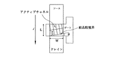
チャンネル領域Iが形成され、ドレーン領域13とチャンネル領域Iの間とソース領域13aとチャンネル領域Iの間には、低濃度の不純物でドーピングされたLDD領域IIが形成されている。
12 バッファー層
13 活性層
14 ゲート絶縁層
15 ゲート電極
16 パッシベーション沿う
17 ソース電極
Claims (6)
- LDD領域、またはオフセット領域を具備している薄膜トランジスターにおいて、
前記LDD、またはオフセット領域ではポリシリコン基板の“プライマリー”結晶粒境界が位置しないことを特徴とする薄膜トランジスター。 - 請求項1に記載の薄膜トランジスターにおいて、
前記LDD領域、またはオフセット領域を含む活性層の幅が“プライマリー”結晶粒境界の間の距離より小さいものである薄膜トランジスター。 - 請求項1に記載の薄膜トランジスターにおいて、
前記ポリシリコン基板は、SLS方法で形成されるものである薄膜トランジスター。 - 請求項1に記載の薄膜トランジスターにおいて、
前記薄膜トランジスターは、液晶表示装置または有機電界発光素子(EL)に使用されるものである薄膜トランジスター。 - 請求項1に記載の薄膜トランジスターにおいて、
前記プライマリー結晶粒境界と前記アクティブチャンネル領域が互いに平行するように配置された薄膜トランジスター。 - 請求1項に記載の薄膜トランジスターにおいて、
前記プライマリー結晶粒境界と前記アクティブチャンネル領域が成す角度が−45°≦θ≦45°である薄膜トランジスター。
Applications Claiming Priority (1)
| Application Number | Priority Date | Filing Date | Title |
|---|---|---|---|
| KR10-2002-0080326A KR100501700B1 (ko) | 2002-12-16 | 2002-12-16 | 엘디디/오프셋 구조를 구비하고 있는 박막 트랜지스터 |
Publications (2)
| Publication Number | Publication Date |
|---|---|
| JP2004200648A true JP2004200648A (ja) | 2004-07-15 |
| JP4361769B2 JP4361769B2 (ja) | 2009-11-11 |
Family
ID=32388328
Family Applications (1)
| Application Number | Title | Priority Date | Filing Date |
|---|---|---|---|
| JP2003297912A Expired - Lifetime JP4361769B2 (ja) | 2002-12-16 | 2003-08-21 | Ldd/オフセット構造を具備している薄膜トランジスター |
Country Status (5)
| Country | Link |
|---|---|
| US (1) | US8314428B2 (ja) |
| EP (1) | EP1432042A3 (ja) |
| JP (1) | JP4361769B2 (ja) |
| KR (1) | KR100501700B1 (ja) |
| CN (1) | CN100474627C (ja) |
Families Citing this family (7)
| Publication number | Priority date | Publication date | Assignee | Title |
|---|---|---|---|---|
| CN100477279C (zh) * | 2006-03-13 | 2009-04-08 | 财团法人工业技术研究院 | 薄膜晶体管结构及其制造方法 |
| CN100499136C (zh) * | 2006-03-22 | 2009-06-10 | 财团法人工业技术研究院 | 具有对称性的薄膜晶体管组件 |
| KR101125565B1 (ko) | 2009-11-13 | 2012-03-23 | 삼성모바일디스플레이주식회사 | 박막트랜지스터, 그를 구비하는 유기전계발광표시장치 및 그들의 제조방법 |
| US8519387B2 (en) * | 2010-07-26 | 2013-08-27 | Semiconductor Energy Laboratory Co., Ltd. | Semiconductor device and method for manufacturing |
| KR102089314B1 (ko) * | 2013-05-14 | 2020-04-14 | 엘지디스플레이 주식회사 | 산화물 박막 트랜지스터 및 그 제조방법 |
| US9761546B2 (en) * | 2015-10-19 | 2017-09-12 | Taiwan Semiconductor Manufacturing Co., Ltd. | Trap layer substrate stacking technique to improve performance for RF devices |
| CN105304500B (zh) * | 2015-10-26 | 2018-01-30 | 深圳市华星光电技术有限公司 | N型tft的制作方法 |
Family Cites Families (27)
| Publication number | Priority date | Publication date | Assignee | Title |
|---|---|---|---|---|
| EP0565231A3 (en) | 1992-03-31 | 1996-11-20 | Sgs Thomson Microelectronics | Method of fabricating a polysilicon thin film transistor |
| JP3182893B2 (ja) * | 1992-07-10 | 2001-07-03 | ソニー株式会社 | 薄膜トランジスタの製造方法 |
| TW226478B (en) * | 1992-12-04 | 1994-07-11 | Semiconductor Energy Res Co Ltd | Semiconductor device and method for manufacturing the same |
| JP3157985B2 (ja) * | 1993-06-10 | 2001-04-23 | 三菱電機株式会社 | 薄膜トランジスタおよびその製造方法 |
| TW395008B (en) * | 1994-08-29 | 2000-06-21 | Semiconductor Energy Lab | Semiconductor circuit for electro-optical device and method of manufacturing the same |
| JPH098314A (ja) | 1995-06-26 | 1997-01-10 | Sharp Corp | 薄膜トランジスタ |
| CA2256699C (en) * | 1996-05-28 | 2003-02-25 | The Trustees Of Columbia University In The City Of New York | Crystallization processing of semiconductor film regions on a substrate, and devices made therewith |
| TW451284B (en) * | 1996-10-15 | 2001-08-21 | Semiconductor Energy Lab | Semiconductor device and method of manufacturing the same |
| JPH11168216A (ja) * | 1997-12-04 | 1999-06-22 | Matsushita Electron Corp | 薄膜トランジスタおよびその製造方法 |
| JPH11354800A (ja) | 1998-06-04 | 1999-12-24 | Hitachi Ltd | 薄膜トランジスタ及びその形成方法並びに液晶表示装置 |
| KR100296110B1 (ko) * | 1998-06-09 | 2001-08-07 | 구본준, 론 위라하디락사 | 박막트랜지스터 제조방법 |
| KR100292048B1 (ko) * | 1998-06-09 | 2001-07-12 | 구본준, 론 위라하디락사 | 박막트랜지스터액정표시장치의제조방법 |
| JP2000208771A (ja) * | 1999-01-11 | 2000-07-28 | Hitachi Ltd | 半導体装置、液晶表示装置およびこれらの製造方法 |
| US6437403B1 (en) * | 1999-01-18 | 2002-08-20 | Sony Corporation | Semiconductor device |
| US7679131B1 (en) * | 1999-08-31 | 2010-03-16 | Semiconductor Energy Laboratory Co., Ltd. | Semiconductor device, manufacturing method thereof, and electronic device |
| KR200171526Y1 (ko) | 1999-09-01 | 2000-03-15 | 권윤노 | 냉동기기용 서비스밸브의 브라켓구조 |
| JP2001127302A (ja) * | 1999-10-28 | 2001-05-11 | Hitachi Ltd | 半導体薄膜基板、半導体装置、半導体装置の製造方法および電子装置 |
| JP2001345451A (ja) * | 2000-05-30 | 2001-12-14 | Hitachi Ltd | 薄膜半導体集積回路装置、それを用いた画像表示装置、及びその製造方法 |
| US6906346B2 (en) * | 2000-07-24 | 2005-06-14 | Matsushita Electric Industrial Co., Ltd. | Semiconductor device, liquid crystal display device, EL display device, method for fabricating semiconductor thin film, and method for manufacturing the semiconductor device |
| US6451631B1 (en) | 2000-08-10 | 2002-09-17 | Hitachi America, Ltd. | Thin film crystal growth by laser annealing |
| KR100737910B1 (ko) * | 2000-11-27 | 2007-07-10 | 삼성전자주식회사 | 폴리실리콘형 박막트랜지스터 제조방법 |
| JP4310076B2 (ja) * | 2001-05-31 | 2009-08-05 | キヤノン株式会社 | 結晶性薄膜の製造方法 |
| KR100543061B1 (ko) * | 2001-06-01 | 2006-01-20 | 엘지.필립스 엘시디 주식회사 | 구동회로부 일체형 액정표시장치용 어레이 기판의 제조방법 |
| JP2003163221A (ja) * | 2001-11-28 | 2003-06-06 | Semiconductor Energy Lab Co Ltd | 半導体装置の作製方法 |
| KR100462862B1 (ko) * | 2002-01-18 | 2004-12-17 | 삼성에스디아이 주식회사 | 티에프티용 다결정 실리콘 박막 및 이를 이용한디스플레이 디바이스 |
| JP4190798B2 (ja) * | 2002-05-08 | 2008-12-03 | Nec液晶テクノロジー株式会社 | 薄膜トランジスタ及びその製造方法 |
| KR100483987B1 (ko) * | 2002-07-08 | 2005-04-15 | 삼성에스디아이 주식회사 | 티에프티용 다결정 실리콘 박막 및 이를 사용한 디바이스 |
-
2002
- 2002-12-16 KR KR10-2002-0080326A patent/KR100501700B1/ko not_active Expired - Lifetime
-
2003
- 2003-08-21 JP JP2003297912A patent/JP4361769B2/ja not_active Expired - Lifetime
- 2003-12-15 EP EP03090437A patent/EP1432042A3/en not_active Ceased
- 2003-12-15 US US10/734,162 patent/US8314428B2/en not_active Expired - Fee Related
- 2003-12-16 CN CNB2003101097792A patent/CN100474627C/zh not_active Expired - Lifetime
Also Published As
| Publication number | Publication date |
|---|---|
| KR100501700B1 (ko) | 2005-07-18 |
| EP1432042A2 (en) | 2004-06-23 |
| JP4361769B2 (ja) | 2009-11-11 |
| US8314428B2 (en) | 2012-11-20 |
| EP1432042A3 (en) | 2007-03-21 |
| US20040124480A1 (en) | 2004-07-01 |
| CN100474627C (zh) | 2009-04-01 |
| CN1512596A (zh) | 2004-07-14 |
| KR20040053868A (ko) | 2004-06-25 |
Similar Documents
| Publication | Publication Date | Title |
|---|---|---|
| US8987120B2 (en) | Flat panel display device comprising polysilicon thin film transistor and method of manufacturing the same | |
| KR101021479B1 (ko) | 박막 트랜지스터, 그의 형성방법 및 박막 트랜지스터를 구비하는 평판 표시장치 | |
| US7812895B2 (en) | Thin film transistor (TFT) array panel with TFTs having varying leakage currents | |
| KR100483985B1 (ko) | 박막 트랜지스터용 다결정 실리콘 박막 및 이를 사용한디바이스 | |
| CN102194886B (zh) | 薄膜晶体管、其制造方法和具有该薄膜晶体管的显示设备 | |
| US8278159B2 (en) | Thin film transistor, method of fabricating the same, and a display device including the thin film transistor | |
| KR20070072207A (ko) | 폴리실리콘 박막트랜지스터를 이용한 액정표시장치 및 그제조 방법 | |
| US20050062047A1 (en) | Transistor substrate, display device, and method of manufacturing transistor substrate and display device | |
| US8110833B2 (en) | Display device with impurities formed within connection regions | |
| JP4361769B2 (ja) | Ldd/オフセット構造を具備している薄膜トランジスター | |
| CN1702879A (zh) | 薄膜晶体管衬底和其制造方法 | |
| US20060131585A1 (en) | Thin film transistor array panel | |
| KR100552958B1 (ko) | 다결정 실리콘 박막 트랜지스터를 포함하는 평판 표시소자 및 그의 제조 방법 | |
| KR100454751B1 (ko) | 듀얼 또는 멀티플 게이트를 사용하는 티에프티의 제조 방법 | |
| KR100534577B1 (ko) | 특성이 우수한 디스플레이 디바이스 | |
| KR100514179B1 (ko) | 박막 트랜지스터 및 이를 사용하는 유기 전계 발광 소자 | |
| KR101483629B1 (ko) | 박막 트랜지스터 및 그 제조방법 | |
| KR100534576B1 (ko) | 다중 게이트를 갖는 박막 트랜지스터 | |
| KR100507345B1 (ko) | 엘디디 구조를 구비하고 있는 박막 트랜지스터 및 이를사용하는 평판 표시 소자 |
Legal Events
| Date | Code | Title | Description |
|---|---|---|---|
| A521 | Request for written amendment filed |
Free format text: JAPANESE INTERMEDIATE CODE: A821 Effective date: 20040602 |
|
| A621 | Written request for application examination |
Free format text: JAPANESE INTERMEDIATE CODE: A621 Effective date: 20040602 |
|
| A977 | Report on retrieval |
Free format text: JAPANESE INTERMEDIATE CODE: A971007 Effective date: 20060223 |
|
| A131 | Notification of reasons for refusal |
Free format text: JAPANESE INTERMEDIATE CODE: A131 Effective date: 20070306 |
|
| A02 | Decision of refusal |
Free format text: JAPANESE INTERMEDIATE CODE: A02 Effective date: 20080805 |
|
| A521 | Request for written amendment filed |
Free format text: JAPANESE INTERMEDIATE CODE: A523 Effective date: 20081104 Free format text: JAPANESE INTERMEDIATE CODE: A821 Effective date: 20081104 |
|
| A711 | Notification of change in applicant |
Free format text: JAPANESE INTERMEDIATE CODE: A712 Effective date: 20081208 |
|
| A521 | Request for written amendment filed |
Free format text: JAPANESE INTERMEDIATE CODE: A523 Effective date: 20090225 |
|
| A911 | Transfer to examiner for re-examination before appeal (zenchi) |
Free format text: JAPANESE INTERMEDIATE CODE: A911 Effective date: 20090312 |
|
| A131 | Notification of reasons for refusal |
Free format text: JAPANESE INTERMEDIATE CODE: A131 Effective date: 20090616 |
|
| A521 | Request for written amendment filed |
Free format text: JAPANESE INTERMEDIATE CODE: A523 Effective date: 20090618 |
|
| TRDD | Decision of grant or rejection written | ||
| A01 | Written decision to grant a patent or to grant a registration (utility model) |
Free format text: JAPANESE INTERMEDIATE CODE: A01 Effective date: 20090714 |
|
| A01 | Written decision to grant a patent or to grant a registration (utility model) |
Free format text: JAPANESE INTERMEDIATE CODE: A01 |
|
| A61 | First payment of annual fees (during grant procedure) |
Free format text: JAPANESE INTERMEDIATE CODE: A61 Effective date: 20090813 |
|
| R150 | Certificate of patent or registration of utility model |
Free format text: JAPANESE INTERMEDIATE CODE: R150 Ref document number: 4361769 Country of ref document: JP Free format text: JAPANESE INTERMEDIATE CODE: R150 |
|
| FPAY | Renewal fee payment (event date is renewal date of database) |
Free format text: PAYMENT UNTIL: 20120821 Year of fee payment: 3 |
|
| FPAY | Renewal fee payment (event date is renewal date of database) |
Free format text: PAYMENT UNTIL: 20130821 Year of fee payment: 4 |
|
| R250 | Receipt of annual fees |
Free format text: JAPANESE INTERMEDIATE CODE: R250 |
|
| FPAY | Renewal fee payment (event date is renewal date of database) |
Free format text: PAYMENT UNTIL: 20130821 Year of fee payment: 4 |
|
| S111 | Request for change of ownership or part of ownership |
Free format text: JAPANESE INTERMEDIATE CODE: R313111 |
|
| FPAY | Renewal fee payment (event date is renewal date of database) |
Free format text: PAYMENT UNTIL: 20130821 Year of fee payment: 4 |
|
| R350 | Written notification of registration of transfer |
Free format text: JAPANESE INTERMEDIATE CODE: R350 |
|
| R250 | Receipt of annual fees |
Free format text: JAPANESE INTERMEDIATE CODE: R250 |
|
| R250 | Receipt of annual fees |
Free format text: JAPANESE INTERMEDIATE CODE: R250 |
|
| R250 | Receipt of annual fees |
Free format text: JAPANESE INTERMEDIATE CODE: R250 |
|
| R250 | Receipt of annual fees |
Free format text: JAPANESE INTERMEDIATE CODE: R250 |
|
| R250 | Receipt of annual fees |
Free format text: JAPANESE INTERMEDIATE CODE: R250 |
|
| R250 | Receipt of annual fees |
Free format text: JAPANESE INTERMEDIATE CODE: R250 |
|
| R250 | Receipt of annual fees |
Free format text: JAPANESE INTERMEDIATE CODE: R250 |
|
| R250 | Receipt of annual fees |
Free format text: JAPANESE INTERMEDIATE CODE: R250 |
|
| R250 | Receipt of annual fees |
Free format text: JAPANESE INTERMEDIATE CODE: R250 |
|
| R250 | Receipt of annual fees |
Free format text: JAPANESE INTERMEDIATE CODE: R250 |
|
| EXPY | Cancellation because of completion of term |