JP2004207731A - 電子デバイスの製造 - Google Patents
電子デバイスの製造 Download PDFInfo
- Publication number
- JP2004207731A JP2004207731A JP2003423432A JP2003423432A JP2004207731A JP 2004207731 A JP2004207731 A JP 2004207731A JP 2003423432 A JP2003423432 A JP 2003423432A JP 2003423432 A JP2003423432 A JP 2003423432A JP 2004207731 A JP2004207731 A JP 2004207731A
- Authority
- JP
- Japan
- Prior art keywords
- lift
- layer
- layers
- polymer
- substrate
- Prior art date
- Legal status (The legal status is an assumption and is not a legal conclusion. Google has not performed a legal analysis and makes no representation as to the accuracy of the status listed.)
- Withdrawn
Links
Images
Classifications
-
- G—PHYSICS
- G03—PHOTOGRAPHY; CINEMATOGRAPHY; ANALOGOUS TECHNIQUES USING WAVES OTHER THAN OPTICAL WAVES; ELECTROGRAPHY; HOLOGRAPHY
- G03F—PHOTOMECHANICAL PRODUCTION OF TEXTURED OR PATTERNED SURFACES, e.g. FOR PRINTING, FOR PROCESSING OF SEMICONDUCTOR DEVICES; MATERIALS THEREFOR; ORIGINALS THEREFOR; APPARATUS SPECIALLY ADAPTED THEREFOR
- G03F7/00—Photomechanical, e.g. photolithographic, production of textured or patterned surfaces, e.g. printing surfaces; Materials therefor, e.g. comprising photoresists; Apparatus specially adapted therefor
- G03F7/004—Photosensitive materials
- G03F7/09—Photosensitive materials characterised by structural details, e.g. supports, auxiliary layers
- G03F7/094—Multilayer resist systems, e.g. planarising layers
-
- H—ELECTRICITY
- H10—SEMICONDUCTOR DEVICES; ELECTRIC SOLID-STATE DEVICES NOT OTHERWISE PROVIDED FOR
- H10D—INORGANIC ELECTRIC SEMICONDUCTOR DEVICES
- H10D64/00—Electrodes of devices having potential barriers
- H10D64/01—Manufacture or treatment
- H10D64/011—Manufacture or treatment of electrodes ohmically coupled to a semiconductor
-
- G—PHYSICS
- G03—PHOTOGRAPHY; CINEMATOGRAPHY; ANALOGOUS TECHNIQUES USING WAVES OTHER THAN OPTICAL WAVES; ELECTROGRAPHY; HOLOGRAPHY
- G03F—PHOTOMECHANICAL PRODUCTION OF TEXTURED OR PATTERNED SURFACES, e.g. FOR PRINTING, FOR PROCESSING OF SEMICONDUCTOR DEVICES; MATERIALS THEREFOR; ORIGINALS THEREFOR; APPARATUS SPECIALLY ADAPTED THEREFOR
- G03F7/00—Photomechanical, e.g. photolithographic, production of textured or patterned surfaces, e.g. printing surfaces; Materials therefor, e.g. comprising photoresists; Apparatus specially adapted therefor
- G03F7/004—Photosensitive materials
- G03F7/09—Photosensitive materials characterised by structural details, e.g. supports, auxiliary layers
- G03F7/11—Photosensitive materials characterised by structural details, e.g. supports, auxiliary layers having cover layers or intermediate layers, e.g. subbing layers
-
- H—ELECTRICITY
- H10—SEMICONDUCTOR DEVICES; ELECTRIC SOLID-STATE DEVICES NOT OTHERWISE PROVIDED FOR
- H10P—GENERIC PROCESSES OR APPARATUS FOR THE MANUFACTURE OR TREATMENT OF DEVICES COVERED BY CLASS H10
- H10P14/00—Formation of materials, e.g. in the shape of layers or pillars
- H10P14/60—Formation of materials, e.g. in the shape of layers or pillars of insulating materials
- H10P14/68—Organic materials, e.g. photoresists
- H10P14/683—Organic materials, e.g. photoresists carbon-based polymeric organic materials, e.g. polyimides, poly cyclobutene or PVC
-
- H—ELECTRICITY
- H10—SEMICONDUCTOR DEVICES; ELECTRIC SOLID-STATE DEVICES NOT OTHERWISE PROVIDED FOR
- H10P—GENERIC PROCESSES OR APPARATUS FOR THE MANUFACTURE OR TREATMENT OF DEVICES COVERED BY CLASS H10
- H10P50/00—Etching of wafers, substrates or parts of devices
- H10P50/71—Etching of wafers, substrates or parts of devices using masks for conductive or resistive materials
-
- H—ELECTRICITY
- H10—SEMICONDUCTOR DEVICES; ELECTRIC SOLID-STATE DEVICES NOT OTHERWISE PROVIDED FOR
- H10P—GENERIC PROCESSES OR APPARATUS FOR THE MANUFACTURE OR TREATMENT OF DEVICES COVERED BY CLASS H10
- H10P50/00—Etching of wafers, substrates or parts of devices
- H10P50/73—Etching of wafers, substrates or parts of devices using masks for insulating materials
-
- H—ELECTRICITY
- H10—SEMICONDUCTOR DEVICES; ELECTRIC SOLID-STATE DEVICES NOT OTHERWISE PROVIDED FOR
- H10P—GENERIC PROCESSES OR APPARATUS FOR THE MANUFACTURE OR TREATMENT OF DEVICES COVERED BY CLASS H10
- H10P76/00—Manufacture or treatment of masks on semiconductor bodies, e.g. by lithography or photolithography
- H10P76/20—Manufacture or treatment of masks on semiconductor bodies, e.g. by lithography or photolithography of masks comprising organic materials
- H10P76/204—Manufacture or treatment of masks on semiconductor bodies, e.g. by lithography or photolithography of masks comprising organic materials of organic photoresist masks
-
- H—ELECTRICITY
- H10—SEMICONDUCTOR DEVICES; ELECTRIC SOLID-STATE DEVICES NOT OTHERWISE PROVIDED FOR
- H10P—GENERIC PROCESSES OR APPARATUS FOR THE MANUFACTURE OR TREATMENT OF DEVICES COVERED BY CLASS H10
- H10P76/00—Manufacture or treatment of masks on semiconductor bodies, e.g. by lithography or photolithography
- H10P76/40—Manufacture or treatment of masks on semiconductor bodies, e.g. by lithography or photolithography of masks comprising inorganic materials
- H10P76/408—Manufacture or treatment of masks on semiconductor bodies, e.g. by lithography or photolithography of masks comprising inorganic materials characterised by their sizes, orientations, dispositions, behaviours or shapes
- H10P76/4085—Manufacture or treatment of masks on semiconductor bodies, e.g. by lithography or photolithography of masks comprising inorganic materials characterised by their sizes, orientations, dispositions, behaviours or shapes characterised by the processes involved to create the masks
Landscapes
- Engineering & Computer Science (AREA)
- Architecture (AREA)
- Structural Engineering (AREA)
- Physics & Mathematics (AREA)
- General Physics & Mathematics (AREA)
- Formation Of Insulating Films (AREA)
- Weting (AREA)
Abstract
【解決手段】
フォトレジストや反射防止コーティングなどの架橋ポリマー層を除去するために使用される強力な化学物質に対して影響されやすい材料の1つ以上の層を含む電子デバイスを製造する方法が提供される。架橋ポリマー層は、基体と架橋ポリマー層との間にある除去自在層を使用することによって、エッチング後に容易に除去することができる。
【選択図】なし
Description
中間層絶縁材料の誘電率を低下させる方法の1つは、絶縁材料としてある有機材料を使用することである。別の方法は、絶縁膜内部、特に無機誘電材料内部に非常に小さく均一に分散した細孔または空隙を混入させることである。このような多孔質誘電材料は、細孔が存在しない同じ誘電材料と比較すると、低下した誘電率を有し、おそらくは実質的に低下した誘電率を有する。
((RR1SiO)a(R2SiO1.5)b(R3SiO1.5)c(SiO2)d))n
の縮合物または加水分解生成物のポリマーであり、式中、R、R1、R2、およびR3は独立に、水素、(C1−C6)アルキル、アリール、および置換アリールから選択され、a、b、cおよびdは独立に0〜1の数であり、nは約3〜約10,000の整数であり、ただし、a+b+c+d=1であり、R、R1、およびR2の少なくとも1つは水素ではない。「置換アリール」は、アリール基の1つ以上の水素が、シアノ、ヒドロキシ、メルカプト、ハロ、(C1−C6)アルキル、(C1−C6)アルコキシなどの別の置換基で置換されたアリール基を意味する。上記式中、a、b、およびcは各成分のモル比を表している。このようなモル比は、0〜約1の間を変動することができる。通常aは0〜約0.8である。一般に、bは約0.2〜約1である。特に、cは0〜約0.8である。より一般的には、dは0〜約0.8である。上記式中、nは繰り返し単位数を意味する。縮合物の場合、nは通常約3〜約1000の整数である。理解されるように、あらゆる硬化ステップの前に、有機ポリシリカ縮合物は、1つ以上のヒドロキシルまたはアルコキシ末端キャッピング基または側鎖官能基を含んでよい。このような末端キャッピング基または側鎖官能基は当業者に公知である。
続いて、フォトレジスト層は、マスクを通して化学線を使用して画像形成される。使用される放射線の選択は、選択された個々のフォトレジストに依存し、当業者の能力の十分範囲内にある。画像形成後、フォトレジスト層が現像されてパターンが形成される。次に、このパターンが、反応性イオンエッチングなどのエッチングなどによって、下にある層に転写される。このようなエッチング法によって、下にある層にアパーチャーが形成される。さらに、このようなエッチングによって、ポストエッチポリマーが形成され、これらのポリマーは特にある種の有機金属種を含有する。
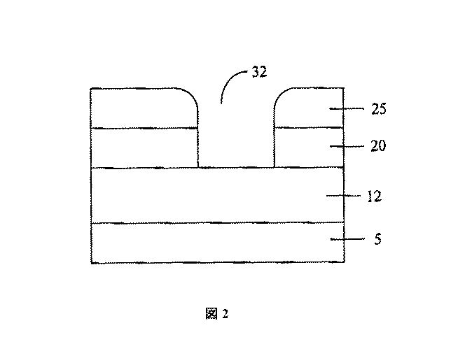
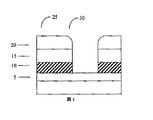
10 強誘電性ポリマー層
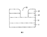
12 低k誘電材料
15 金属層
20 リフトオフ層
25 フォトレジスト層
30 アパーチャー
32 アパーチャー
Claims (10)
- 集積回路デバイスの製造方法であって、a)1つ以上のリフトオフ層を基体上に配置するステップと、b)架橋コーティングの1つ以上の層を前記リフトオフ層上に配置するステップと、c)前記基体にパターン形成するステップと、d)前記コーティングおよびリフトオフ層を除去するステップとを含み、前記基体は、強誘電性ポリマー、誘電材料、またはその両方の1つ以上の層を含み、前記誘電材料は誘電率≦3を有し、前記リフトオフ層は有機ポリマー材料である製造方法。
- 前記リフトオフ層がポリグルタルイミドを含む請求項1記載の方法。
- 前記ポリグルタルイミドが≦50,000の分子量を有する請求項2記載の方法。
- 前記リフトオフ層が光吸収性材料をさらに含む請求項1から3のいずれか1項記載の方法。
- 前記リフトオフ層が架橋ポリマー粒子を含む請求項1から4のいずれか1項記載の方法。
- 前記誘電材料が≦2.8の誘電率を有する請求項1から5のいずれか1項記載の方法。
- 前記リフトオフ層が、溶剤との接触によって除去される請求項1から6のいずれか1項記載の方法。
- 前記リフトオフ層が≦2500Åの厚さを有する請求項1から7のいずれか1項記載の方法。
- 強誘電性ポリマー、誘電率≦3を有する誘電材料、またはその両方の1つ以上の層と、1つ以上のリフトオフ層と、前記リフト層上の架橋コーティングの1つ以上の層とを含む集積回路デバイスであって、前記リフトオフ層が有機ポリマー材料である集積回路デバイス。
- 誘電材料が、誘電率≦3を有する請求項13記載の集積回路デバイス。
Applications Claiming Priority (1)
| Application Number | Priority Date | Filing Date | Title |
|---|---|---|---|
| US43597502P | 2002-12-20 | 2002-12-20 |
Publications (2)
| Publication Number | Publication Date |
|---|---|
| JP2004207731A true JP2004207731A (ja) | 2004-07-22 |
| JP2004207731A5 JP2004207731A5 (ja) | 2007-02-08 |
Family
ID=32393634
Family Applications (1)
| Application Number | Title | Priority Date | Filing Date |
|---|---|---|---|
| JP2003423432A Withdrawn JP2004207731A (ja) | 2002-12-20 | 2003-12-19 | 電子デバイスの製造 |
Country Status (6)
| Country | Link |
|---|---|
| US (1) | US7056824B2 (ja) |
| EP (1) | EP1431823A2 (ja) |
| JP (1) | JP2004207731A (ja) |
| KR (1) | KR20040055685A (ja) |
| CN (1) | CN1521565A (ja) |
| TW (1) | TWI248138B (ja) |
Cited By (3)
| Publication number | Priority date | Publication date | Assignee | Title |
|---|---|---|---|---|
| JP2012526399A (ja) * | 2009-05-08 | 2012-10-25 | 1366 テクノロジーズ インク. | 堆積膜の選択的除去のための多孔質リフトオフ層 |
| JP2022550171A (ja) * | 2019-09-30 | 2022-11-30 | バーサム マテリアルズ ユーエス,リミティド ライアビリティ カンパニー | 半導体素子製造時に窒化ケイ素を選択的に除去するためのエッチング組成物及びエッチング方法 |
| US12281251B2 (en) | 2019-09-30 | 2025-04-22 | Versum Materials Us, Llc | Etching composition and method for selectively removing silicon nitride during manufacture of a semiconductor device |
Families Citing this family (11)
| Publication number | Priority date | Publication date | Assignee | Title |
|---|---|---|---|---|
| US7119031B2 (en) * | 2004-06-28 | 2006-10-10 | Micron Technology, Inc. | Methods of forming patterned photoresist layers over semiconductor substrates |
| US20060000493A1 (en) * | 2004-06-30 | 2006-01-05 | Steger Richard M | Chemical-mechanical post-etch removal of photoresist in polymer memory fabrication |
| US7846017B2 (en) * | 2004-07-06 | 2010-12-07 | Igt | Methods and apparatus for facilitating remote viewing of gaming outcomes |
| US7090782B1 (en) * | 2004-09-03 | 2006-08-15 | Lam Research Corporation | Etch with uniformity control |
| US20060105567A1 (en) * | 2004-11-12 | 2006-05-18 | Intel Corporation | Method for forming a dual-damascene structure |
| US20060183055A1 (en) * | 2005-02-15 | 2006-08-17 | O'neill Mark L | Method for defining a feature on a substrate |
| US7753797B2 (en) * | 2005-03-18 | 2010-07-13 | Igt | Security methods and apparatus for a tangible medium containing wagering game outcomes |
| US20070286941A1 (en) * | 2006-06-13 | 2007-12-13 | Bin Huang | Surface treatment of a polymeric stent |
| US7998524B2 (en) | 2007-12-10 | 2011-08-16 | Abbott Cardiovascular Systems Inc. | Methods to improve adhesion of polymer coatings over stents |
| US9102901B2 (en) * | 2012-12-20 | 2015-08-11 | Rohm And Haas Electronic Materials Llc | Methods and compositions for removal of metal hardmasks |
| KR102053921B1 (ko) * | 2019-03-13 | 2019-12-09 | 영창케미칼 주식회사 | 반도체 제조 공정에 있어서 식각 패턴 신규 형성 방법 |
Family Cites Families (14)
| Publication number | Priority date | Publication date | Assignee | Title |
|---|---|---|---|---|
| US4246374A (en) | 1979-04-23 | 1981-01-20 | Rohm And Haas Company | Imidized acrylic polymers |
| US4451971A (en) | 1982-08-02 | 1984-06-05 | Fairchild Camera And Instrument Corporation | Lift-off wafer processing |
| US4524121A (en) | 1983-11-21 | 1985-06-18 | Rohm And Haas Company | Positive photoresists containing preformed polyglutarimide polymer |
| US4636532A (en) | 1985-10-11 | 1987-01-13 | Shipley Company Inc. | Method for preparing polyglutarimide having a lower molecular weight and a low polydispersity |
| US5731385A (en) | 1993-12-16 | 1998-03-24 | International Business Machines Corporation | Polymeric dyes for antireflective coatings |
| EP0690494B1 (de) * | 1994-06-27 | 2004-03-17 | Infineon Technologies AG | Verbindungs- und Aufbautechnik für Multichip-Module |
| US5944975A (en) | 1996-03-26 | 1999-08-31 | Texas Instruments Incorporated | Method of forming a lift-off layer having controlled adhesion strength |
| TW476019B (en) * | 1999-05-27 | 2002-02-11 | Winbond Electronics Corp | Method for forming crosslinking photoresist |
| US6805139B1 (en) * | 1999-10-20 | 2004-10-19 | Mattson Technology, Inc. | Systems and methods for photoresist strip and residue treatment in integrated circuit manufacturing |
| US6352909B1 (en) | 2000-01-06 | 2002-03-05 | Silicon Wafer Technologies, Inc. | Process for lift-off of a layer from a substrate |
| NO20005980L (no) | 2000-11-27 | 2002-05-28 | Thin Film Electronics Ab | Ferroelektrisk minnekrets og fremgangsmåte ved dens fremstilling |
| US6798003B2 (en) * | 2001-07-20 | 2004-09-28 | Intel Corporation | Reliable adhesion layer interface structure for polymer memory electrode and method of making same |
| JP3810309B2 (ja) * | 2001-12-03 | 2006-08-16 | Necエレクトロニクス株式会社 | 半導体装置の製造方法 |
| US6878500B2 (en) | 2002-04-06 | 2005-04-12 | Marlborough, | Stripping method |
-
2003
- 2003-12-19 JP JP2003423432A patent/JP2004207731A/ja not_active Withdrawn
- 2003-12-19 US US10/742,424 patent/US7056824B2/en not_active Expired - Fee Related
- 2003-12-19 KR KR1020030093626A patent/KR20040055685A/ko not_active Withdrawn
- 2003-12-19 CN CNA2003101249615A patent/CN1521565A/zh active Pending
- 2003-12-19 TW TW092136108A patent/TWI248138B/zh not_active IP Right Cessation
- 2003-12-19 EP EP03258045A patent/EP1431823A2/en not_active Withdrawn
Cited By (4)
| Publication number | Priority date | Publication date | Assignee | Title |
|---|---|---|---|---|
| JP2012526399A (ja) * | 2009-05-08 | 2012-10-25 | 1366 テクノロジーズ インク. | 堆積膜の選択的除去のための多孔質リフトオフ層 |
| JP2022550171A (ja) * | 2019-09-30 | 2022-11-30 | バーサム マテリアルズ ユーエス,リミティド ライアビリティ カンパニー | 半導体素子製造時に窒化ケイ素を選択的に除去するためのエッチング組成物及びエッチング方法 |
| JP7566895B2 (ja) | 2019-09-30 | 2024-10-15 | バーサム マテリアルズ ユーエス,リミティド ライアビリティ カンパニー | 半導体素子製造時に窒化ケイ素を選択的に除去するためのエッチング組成物及びエッチング方法 |
| US12281251B2 (en) | 2019-09-30 | 2025-04-22 | Versum Materials Us, Llc | Etching composition and method for selectively removing silicon nitride during manufacture of a semiconductor device |
Also Published As
| Publication number | Publication date |
|---|---|
| KR20040055685A (ko) | 2004-06-26 |
| TW200414375A (en) | 2004-08-01 |
| TWI248138B (en) | 2006-01-21 |
| US7056824B2 (en) | 2006-06-06 |
| US20040224528A1 (en) | 2004-11-11 |
| CN1521565A (zh) | 2004-08-18 |
| EP1431823A2 (en) | 2004-06-23 |
Similar Documents
| Publication | Publication Date | Title |
|---|---|---|
| US5527872A (en) | Electronic device with a spin-on glass dielectric layer | |
| US5470693A (en) | Method of forming patterned polyimide films | |
| US4430153A (en) | Method of forming an RIE etch barrier by in situ conversion of a silicon containing alkyl polyamide/polyimide | |
| US7056824B2 (en) | Electronic device manufacture | |
| JP6458799B2 (ja) | パターン形成方法 | |
| JP3951124B2 (ja) | 絶縁膜 | |
| JP2005519481A5 (ja) | ||
| JPWO1999052136A1 (ja) | 配線構造体の製造方法 | |
| WO2010010928A1 (ja) | コーティング組成物及びパターン形成方法 | |
| KR20070085174A (ko) | 리소그래피 공정용 탑 코트 | |
| WO2015146524A1 (ja) | パターン形成方法 | |
| WO2010032796A1 (ja) | サイドウォール形成用組成物 | |
| JP2001098224A (ja) | シリカ系被膜、シリカ系被膜の形成方法及びシリカ系被膜を有する電子部品 | |
| JPH0527444A (ja) | シリカ基材非反射性平面化層 | |
| WO2006030641A1 (ja) | 反射防止膜形成用組成物およびこれを用いた配線形成方法 | |
| JP2001098218A (ja) | シリカ系被膜、シリカ系被膜の形成方法及びシリカ系被膜を有する電子部品 | |
| CN100552542C (zh) | 由旋涂上的陶瓷薄膜组成的构图层 | |
| Strandjord et al. | Photosensitive benzocyclobutene for stress-buffer and passivation applications (one mask manufacturing process) | |
| WO2009096480A1 (ja) | ハードマスク用除去組成物および除去方法 | |
| US5087553A (en) | Method for transferring patterns on silicone ladder type resin and etching solution used in such method | |
| JP2000058540A (ja) | 低誘電率絶縁膜形成用組成物および低誘電率絶縁膜形成方法 | |
| JP2000021872A (ja) | 低誘電率樹脂組成物、低誘電率絶縁膜形成方法および半導体装置の製造方法 | |
| JPH06244171A (ja) | 層間絶縁膜形成用塗布液およびこれを用いた層間絶縁膜形成方法 | |
| CN107430334A (zh) | 正型感光性树脂组合物、图案固化膜的制造方法、图案固化膜和电子部件 | |
| JPH08191069A (ja) | Si含有薄膜の形成方法 |
Legal Events
| Date | Code | Title | Description |
|---|---|---|---|
| A521 | Request for written amendment filed |
Free format text: JAPANESE INTERMEDIATE CODE: A523 Effective date: 20061016 |
|
| A521 | Request for written amendment filed |
Free format text: JAPANESE INTERMEDIATE CODE: A523 Effective date: 20061218 |
|
| A621 | Written request for application examination |
Free format text: JAPANESE INTERMEDIATE CODE: A621 Effective date: 20061218 |
|
| RD02 | Notification of acceptance of power of attorney |
Free format text: JAPANESE INTERMEDIATE CODE: A7422 Effective date: 20061218 |
|
| A761 | Written withdrawal of application |
Free format text: JAPANESE INTERMEDIATE CODE: A761 Effective date: 20090224 |
|
| RD02 | Notification of acceptance of power of attorney |
Free format text: JAPANESE INTERMEDIATE CODE: A7422 Effective date: 20090224 |