JP2004509472A - レーザ熱加工用の熱誘導位相切替 - Google Patents
レーザ熱加工用の熱誘導位相切替 Download PDFInfo
- Publication number
- JP2004509472A JP2004509472A JP2002527866A JP2002527866A JP2004509472A JP 2004509472 A JP2004509472 A JP 2004509472A JP 2002527866 A JP2002527866 A JP 2002527866A JP 2002527866 A JP2002527866 A JP 2002527866A JP 2004509472 A JP2004509472 A JP 2004509472A
- Authority
- JP
- Japan
- Prior art keywords
- layer
- phase
- temperature
- phase switching
- radiation
- Prior art date
- Legal status (The legal status is an assumption and is not a legal conclusion. Google has not performed a legal analysis and makes no representation as to the accuracy of the status listed.)
- Granted
Links
Images


Classifications
-
- H—ELECTRICITY
- H10—SEMICONDUCTOR DEVICES; ELECTRIC SOLID-STATE DEVICES NOT OTHERWISE PROVIDED FOR
- H10P—GENERIC PROCESSES OR APPARATUS FOR THE MANUFACTURE OR TREATMENT OF DEVICES COVERED BY CLASS H10
- H10P34/00—Irradiation with electromagnetic or particle radiation of wafers, substrates or parts of devices
- H10P34/40—Irradiation with electromagnetic or particle radiation of wafers, substrates or parts of devices with high-energy radiation
- H10P34/42—Irradiation with electromagnetic or particle radiation of wafers, substrates or parts of devices with high-energy radiation with electromagnetic radiation, e.g. laser annealing
-
- G—PHYSICS
- G03—PHOTOGRAPHY; CINEMATOGRAPHY; ANALOGOUS TECHNIQUES USING WAVES OTHER THAN OPTICAL WAVES; ELECTROGRAPHY; HOLOGRAPHY
- G03G—ELECTROGRAPHY; ELECTROPHOTOGRAPHY; MAGNETOGRAPHY
- G03G5/00—Recording-members for original recording by exposure, e.g. to light, to heat or to electrons; Manufacture thereof; Selection of materials therefor
- G03G5/16—Layers for recording by changing the magnetic properties, e.g. for Curie-point-writing
Landscapes
- Physics & Mathematics (AREA)
- General Physics & Mathematics (AREA)
- Recrystallisation Techniques (AREA)
- Thin Film Transistor (AREA)
Abstract
Description
本発明はレーザ熱加工に関し、特に、短パルスの放射エネルギーを使用して、加工対象であるワークピースの最高温度を精密に制御する方法および装置に関する。
【0001】
(背景技術)
レーザ熱加工(LTP)は、半導体デバイスの製造において、半導体ウェハなどのワークピースを加工するために使用される。このような加工によって、非常に低いシート抵抗および非常に浅い接合部を有するトランジスタを製造することが可能になり、この結果、半導体デバイス(例えば、集積回路または「IC」)の性能がより向上する(例えば、速度が速くなる)。
【0002】
半導体製造に応用されるLTP方法のうち1つの方法では、短パルスのレーザを使用して、トランジスタのソースおよびドレインを熱でアニールし、注入されたドーパントを活性化する。条件が適切であれば、固体融解限度より上の活性化されたドーパントレベルを有するソース接合部およびドレイン接合部を作成することができる。これによって、速度が速く駆動電流が高いトランジスタが作成される。この技術は、「Fabrication Method for Reduced Dimension FET Devices」という名称の米国特許第5,908,307号に開示され、この特許は参照により本明細書に組み込まれている。
【0003】
単一トランジスタにLTPを実行することで性能の向上を達成することが、ICに有利であると期待されている。残念なことに、LTPを、単一のトランジスタの製造から完全な集積回路の製造へ拡大することは困難である。LTPプロセスの有する加工枠は非常に狭く(すなわち、損傷を起こさずにトランジスタを活性化させるレーザのエネルギーの範囲が狭い)、各トランジスタに送る(そして各トランジスタが吸収する)絶対エネルギーには、相当な均一性、安定性、再現性が必要である。
【0004】
最近のICは種々のデバイス構成と材料を含むので、含まれる熱質量も異なる。各トランジスタにおいて均一な性能を達成するためには、すべてのトランジスタを本質的に同じ温度に熱する(アニールする)ことが必要である。このことによって、回路内の各トランジスタに送られるレーザエネルギーの許容範囲に制限が生じる。この結果、2つの問題が生じる。第1の問題は、均一な加熱を達成するために、十分に均一な暴露(空間的時間的に)を行なうことが困難であることである。第2の問題は、異なるデバイス構成の熱質量が、ドープされた領域(接合部)の局所温度に影響を与えるので、デバイス構成が異なると、必要な入射レーザエネルギーの量が異なることである。
【0005】
これら2つの問題のうち、より困難なのは、局所トランジスタ密度の影響である。今日のほとんどの集積回路は、回路全体にわたって種々のトランジスタ密度を有する。このばらつきは、LTPプロセスに2つの影響を与える。第1の影響は、局所反射率が空間的に異なるので、均一に照射しても局所的に吸収される熱の量が異なるということである。第2の影響は、局所的な熱質量が空間的に異なるということである。熱質量が大きくなると、必要なアニール温度に達するためにより多くのレーザエネルギーを吸収しなければならない。この結果、局所的な熱質量の変化によって、アニーリングを適切に行うために必要な、吸収されるレーザエネルギーの量を変えることが必要となる。完全に均一に照射しても、単一のICまたは別のIC上の異なるトランジスタの間で、大幅な温度のばらつきが生じる可能性がある。このため、単一のIC全体および製造ライン全体を通じて、トランジスタの性能に好ましくないばらつきが生じることになる。
【0006】
原理的には、より高い密度領域ではレーザのフルエンスをより増大させた暴露を調節することによって、デバイス全体でトランジスタ密度の高い場所を補償することが可能である。しかしながら、このためには、加工対象のデバイス各々について、デバイス全体にわたって正確な回路レイアウトを知る必要があり、かつ、回路層に適合させるために、暴露の空間的な放射照度の分布を正確に調節することが必要となる。この努力が達成できたとしても、複雑な装置と多大な費用が必要となるであろう。
【0007】
(発明の開示)
本発明はレーザ熱加工に関し、特に、短パルスの放射エネルギーを用いて加工されるワークピースの最高温度を精密に制御する方法および装置に関する。
【0008】
本発明は、シリコンウェハなどのワークピースに伝えられる熱の量を制御する熱誘導位相「切替」を導入することによって、放射を使用して加工されるワークピースの加熱が不均一であるという問題を解決する。この位相切替層は、下にあるワークピースの1つまたは複数の加工領域が既定の温度に達すると、切替が位相を変えて余計なエネルギーを吸収するように設計された材料からなる1つまたは複数の層を含む。この既定の温度は例えば、加工領域が活性化される温度であってもよい。例えば、下にある1つまたは複数の領域は、トランジスタのソース領域およびドレイン領域、または接合部のドーピングされる領域であってもよく、また、既定の温度はこの領域の活性化温度であってもよい。臨界切替温度に達すると、加工領域の上にある位相切替層の部分が位相を変える。位相を変えることによって位相切替層は温度を変えずに熱を吸収することができる。これにより、下にある加工領域の温度が最高温度にまでさらに上昇することが限定される。
【0009】
本発明を、半導体の製造と、トランジスタを有するICデバイスの形成に適用する時、既定の温度は、トランジスタのソース−ドレイン領域内のアモルファスシリコンが1100〜1410℃の間の温度に達する温度となる。この温度の範囲では、アモルファスシリコンは融解し、ドーパントが活性化する。これらの温度は十分に低いので、下にある結晶シリコン基板は融解せず、このことはデバイスの性能から見ると好ましい。本発明の位相切替は、ウェハの局所領域が実質的に既定の温度を超えることを防ぐ。これにより、他の方法では、放射エネルギーパルスのマグニチュードの変動または形状のばらつきから生じるか、または、放射ビームの空間的な均一性が欠如していることから生じるか、トランジスタ密度が異なることに起因して場所ごとに熱質量にばらつきがあることから生じる可能性のある、種々の望ましくない影響が除去される。
【0010】
(発明を実施するための最良の形態)
本発明はレーザ熱加工に関し、特に、短パルスの放射エネルギーを用いて加工されるワークピースの最高温度を精密に制御する方法および装置に関する。
【0011】
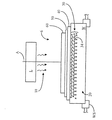
図1から図3に、接合部またはトランジスタなどの半導体デバイスを製造するプロセスの一部として、半導体基板(ワークピース)を加工することに関する位相切替の基本的な概念を示す。図1では、パルス放射源Lからの放射エネルギー10(光子、電子、イオン、中性原子など)を使用して加工されるワークピースとして、シリコン半導体ウェハW上に形成されたフィルムスタック6が示されている。図1に示されるように、ウェハWは、放射源L、および、フィルムスタック6、ウェハWが軸Aに沿って配置されるように、ウェハ支持部材WSによって支持される。放射10は、300と1100nmとの間の波長を有するパルスのレーザ光であってもよい。放射源Lのための適切なレーザ光源は、1064nmで動作するYAGレーザ、532nmで動作する周波数二重(frequency−doubled)YAGレーザ、および700nmと800nmの間で動作するアレクサンドライトレーザ(Alexandrite laser)を含む。適切な放射パルスの長さは1ナノ秒から1マイクロ秒の範囲であり、適切なエネルギーレベルは0.1J/cm2から10J/cm2の範囲である。
【0012】
ウェハWは結晶シリコン領域20を含み、この結晶シリコン領域20中に、ドーパント34を有するドーピングされたアモルファスシリコン領域30が形成される。説明のために、ドーピングされたアモルファス領域30は単一のドーピングされた領域と考える。しかしながら、ドーピングされたアモルファス領域30は、本明細書では「加工領域」と称される、加工される領域の1つの例を示す。例えば、ウェハWは複数のドーピングされたアモルファス領域30を含んでいてもよいし、または、それぞれトランジスタのソース領域とドレイン領域としての機能を有する、正にドーピングされた1つの領域と負にドーピングされた1つの領域とを含んでいてもよい。ウェハWは最高許容温度を有し、最高許容温度はウェハWの融解温度TMであってもよいし、または、温度がこれ以上に上昇するとウェハの機能がなくなるかまたはドーピングされた領域で好ましくない拡散が生じる温度など、別の温度であってもよい。
【0013】
続いて図1を参照すると、ドーピングされたアモルファス領域30は、SiまたはGeのイオンを、ウェハWにおいて数オングストロームから約1000オングストロームの範囲の目標の深さに注入することによって形成することができる。この注入プロセスによって、結晶領域20の基板結晶構造は、イオンが注入される領域がアモルファスになるところまで不規則になる。注入されるイオン種は、Si、Ge、Ar、As、P、Xe、Sb、およびInであってよい。アモルファス化に用いるドーパントの注入は、カリフォルニア州サンタクララのアプライドマテリアル社から市販されている、9500XR ION IMPLANTER(商標)などの既知の装置で行うことができる。
【0014】
ついで、イオン注入機から、p型のドーパントイオン(例えば、ホウ素、アルミニウム、ガリウム、ベリリウム、マグネシウム、亜鉛)または、n型のドーパントイオン(例えば、リン、砒素、アンチモン、ビスマス、セレン、テルル)を使用して、第2のドーパントイオン注入を行う。イオンは所定のエネルギーレベルに加速され(例えば、200eVから40KeV)、予めアモルファス化された領域に所与の照射量で注入され(例えば、約1×10¹⁴atoms/cm2から1×1016atoms/cm2)、これにより、ドーピングされたアモルファス領域30が形成される。実際には典型的には、ウェハW内でのアモルファス領域のドーパントの濃度は深さに応じて段階的に異なる。本実施形態の第1のステップと第2のステップは相互に交換しても同じ効果が得られ、または、ドーパント注入が結晶領域20をアモルファス化するのであれば単一のステップで実行してもよい。
【0015】
アモルファスシリコン領域30の上には吸収層50が堆積され、吸収層50は入射放射線を吸収し、吸収した前記放射線を熱に変換することができる材料を含む。吸収層50は、高温、すなわち、結晶シリコン融解温度である1410℃を超える温度に耐えられなければならない。吸収層50を構成する材料はまた、下の層または領域に影響を与えずに容易に除去できるものでなければならない。吸収層50の役割の1つは、加工の間ウェハWの中かまたは上にあるデバイスの物理的な構造を維持することである。吸収層50の材料の例は、スパッタリングまたはCVD法によって、100オングストロームと5000オングストロームの間の厚さに堆積されたタンタル(Ta)である。吸収層50の他の好ましい材料は、チタン(Ti)、窒化チタン(TiN)、窒化タンタル(TaN)、窒化タングステン(WN)、二酸化珪素、窒化珪素、またはこれらの組み合わせを含む。二酸化珪素層または窒化珪素層は、吸収層材料(すなわち金属と半導体の間)によるウェハWの汚染を防ぐため、または、吸収層とウェハ表面との間の温度低下を提供するために、吸収層の一部として堆積させる必要がある。
【0016】
オプションとして、薄くて剥離可能な層40を、吸収層50とアモルファスシリコン領域30との間に挟んで、LTPを行った後に吸収層を容易に剥がすことができるようにすることもできる。剥離層40の材料の例としては、二酸化珪素と窒化珪素が含まれ、これらはスパッタリングまたはCVD法で堆積させることができる。
【0017】
さらにフィルムスタック6には、吸収層50の上に形成された位相切替層60が含まれる。層60の性質は、位相遷移温度TPにおいて、層60の位相が第1の位相(例えば固体)から第2の位相(例えば液体または気体)に変化するような性質である。この位相遷移温度TPにおいては、位相切替層60の温度をさらに大幅に上げることなく多量の熱が吸収される。
【0018】
位相切替層60は、単一のフィルム層を含んでもよいし、または、多数のフィルム層を含んでいてもよい(すなわち、1層または多層のフィルム層)。図2を参照すると、1実施形態では、位相切替層60は、第1の断熱層62と、第1の断熱層の上に形成された第2の位相遷移層64とを含む。断熱層62の好ましい材料には、二酸化珪素および窒化珪素が含まれ、位相遷移層64の好ましい材料には、ポリイミドとアルミニウム砒素が含まれる。
【0019】
本発明の好ましい実施形態では、層60は約10nmから20ミクロン(「μm」)の範囲の厚さを有する。
【0020】
(動作の方法)
本発明の動作は次の通りである。図1と図2を参照すると、ウェハWの加工は、ドーピングされたアモルファス領域30を活性化するために、放射パルス10を軸Aに沿ってフィルムスタック6に向けることによって行われる。この例では、位相切替層60はまず、実質的に透過性であり、入射吸収層50の上にある。したがって、レーザ放射10のほとんどは層60を通過し、吸収層50に入射する。放射10が層50に吸収されることにより、この層を熱する。吸収層50が加熱される結果、ドーピングされたアモルファス領域30および位相切替層60も加熱される。ドーピングされたアモルファス領域30はこのようにして、活性化温度TA(ドーピングされたシリコンでは、1100℃と1410℃の間)にまで加熱され、位相切替層60も位相遷移温度TPまで加熱される。活性化温度TA(または活性化温度の範囲)になると、ドーパント34はラティスサイト(lattice sites)に組み込まれ、「活性化」される。しかしながら、吸収層50に入射するレーザ放射が多すぎると、位相切替層60がなければ、アモルファス層30は融解するまで加熱されてしまう。この時、本発明では、上記のように、ワークピース(ウェハW)がワークピース(ウェハ)の最高許容温度に達することまたはこの最高許容温度を超えることを防ぐことができる。ワークピース(ウェハ)の最高許容温度、またはこれ以上の温度は、ワークピースに望ましくない影響を与える(例えば融解する)。融解すると、ドーピングされたアモルファス領域30がトランジスタのソース領域またはドレイン領域を構成する場合、ドーピングされたアモルファス領域30の性質に悪影響を与える可能性があるため、融解は好ましくない。融解はまた、トランジスタのゲート領域(図示せず)をも損傷する可能性がある。
【0021】
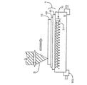
次に6を参照すると、狭いビームの放射B(図3を参照のこと)でワークピースW全体を走査し、基板上の任意のポイント(またはライン)で、短いパルスの放射を生成する。ビームBの焦点を絞って、走査ビームに適したポイント放射、ライン放射、または狭い領域の放射を形成することができる。図3では、吸収層50はフィルムスタック6の上にあり、位相変化層60は吸収層とオプションの層40の間に挟まれている。この構成では、位相変化層60は吸収層の下にあるので、位相変化層は放射エネルギーに対して透過的である必要はない。場合によっては、位相変化層60が、図1および図2のビームBまたは放射10の入射放射線に対して十分に不透過である場合、吸収層50を使用する必要がない場合もある。例えば、入射放射線10(またはビームB)が電子、イオン、または中性原子の粒子からなる場合は、どの場合でも完全に吸収されるので、吸収層はなくてもよい。位相変化層60の位置にかかわらず、基本的な原理は同じである。位相変化層60の最高温度は、入射放射線パルスのエネルギーの幅広い変動に渡って、位相変化の潜熱によって限定される。位相変化の温度はまた、ワークピースの最高温度も限定する。
【0022】
図4は、上記のアニーリング加工の間のドーピングされたアモルファス領域30の温度T30を示す。温度T30は、放射エネルギーに暴露されている間、時間の関数として上昇する。限定がなければ、点線Dに示されるように、結晶シリコンについては、温度T30は融点TM=1410℃まで上昇する。しかしながら、位相切替層60が存在すると(図2を参照)、位相遷移層64の温度T64は、領域30の温度T30とともに上昇する。したがって、層62および/または層40の厚さと熱特性を調節することによって、位相遷移層64が温度T30より高いまたは低い温度になるように設計することができる。図4は、層62の熱伝導性が層40の熱伝導性より大きいため、位相遷移層64の温度T64が加工領域30の温度T30よりも高い場合を示す。
【0023】
上記のように、位相切替層が2つの層62,64を含む場合、位相遷移温度TPを調節することには、以下に詳述する方法にて層62の厚さを調節することが含まれる場合がある。図4のT64カーブが突然平らになることで示されるように、位相遷移層64が位相遷移温度TPに達すると、この層は加熱することなくエネルギーを吸収する。位相遷移層64がポリイミドで作成されている場合、固体層(すなわち第1の位相)から気体層(すなわち第2の位相)への遷移は、TP=1480℃で生じる。したがって、層30の温度T30に対する層64の温度T64のタイミングまたはトラッキングは、層62および層40の熱伝導性と厚さとを調節することによって行われる。位相切替層60を適切に設計することで、層60が十分なエネルギーを吸収して、加工領域30が既定の温度(例えば、融解温度TM)を超えることを防ぐ。
【0024】
(位相切替層の設計)
位相切替層60は次のように設計する。このプロセスは、使用する作動放射タイプおよびパルス長を選択することで開始する。例えば、所定の半導体製造用途では、波長532nmの光放射と、20ナノ秒(ns)のパルス長とを選択してもよい。次のステップは、吸収層50のタイプと、場合によっては、オプションの剥離可能層40のタイプを選択することである。典型的には、剥離可能層40は10〜20nmの二酸化珪素または窒化珪素であり、吸収層50は10〜500nmのチタン、窒化チタン、タンタル、窒化タンタル、タングステン(W)、またはこれらの層の組み合わせであってもよい。吸収層50の目的は、入射するレーザ放射線10を吸収することなので、入射放射線の約75%を超える量を十分に吸収する材料を使用しなければならない。この例においては、層40として厚さ10nmの酸化物、層50として厚さ40nmのタンタルが適切な選択である。
【0025】
次に、層62の任意の厚さを選択する。適切な材料は、二酸化珪素または窒化珪素のいずれかである。この例に関しては、40nmの二酸化珪素が適切な選択である。最後に、層64については100nmの厚さを選択する。位相遷移層64用の適切な材料は、ポリイミドまたはアルミニウム砒素など、位相遷移に関連して高い潜熱を示し、約1000℃から3000℃の間の位相遷移温度TPを有する任意の材料である。この例では、100nmのポリイミドを含む位相遷移層64が適切な選択である。位相変化層64の厚さは、入射放射線エネルギーパルスの反射を最少にする、すなわち、反射防止膜としての役割を果たすように調節することができる。
【0026】
カリフォルニア州リバモアのローレンスリバモア国立研究所からのTOPAZなどの熱移動コードを使用して、パルス放射の間における、フィルムスタック6とその下にある層30の熱挙動を計算することができる。特に、領域(層)30に対する層64の温度を計算し、プロットする。領域30が活性化温度TAに達した時(または活性化温度範囲になった時)、同時に、層64が位相遷移温度TPに達するまで、層62および層40の厚さは変えられる。これによって、領域30が活性化された後、層64は、さらに温度を上げることなく余分な熱を吸収し始める。層64がポリイミドを含む場合、吸収されたエネルギーはポリイミドの気化に使用される。上記の例で、532nmの入射波長と、20nsのパルス長に関して最適なスタックを計算する。
【0027】
層40:二酸化珪素:10nm
層50:タンタル:40nm
層62:二酸化シリコン:
層64:ポリイミド:100nm
この材料のスタックで、位相遷移温度TPは約1480℃であり、これは領域30が約1410℃の活性化温度TAに到達した時に達成される。
【0028】
したがって、位相切替層60は、ドーピングされたアモルファス領域30が活性化温度TA=1100℃に達した後、約1410℃の融解温度TMに達した時または達する前に、位相遷移層64が位相遷移温度TPに達するように設計される。これは、前述したように、断熱層62,40を適切に設計することによって達成される。位相遷移層64が第1の状態から第2の状態に遷移すると、入射レーザ放射10からの熱は層64の温度を上昇させることなく吸収される。これによって、吸収層50のさらなる温度上昇が抑制され、これによって、ドーピングされたアモルファス領域30のさらなる温度上昇も抑制される。一般に、位相切替層60は、周囲の領域(例えば、結晶領域20)を融解させることなく、加工領域30を活性化するために、位相を変えるように設計される。
【0029】
また、多層を含む位相切替層60に関しては、位相切替層60のうち1層だけが、位相を変える層(すなわち「位相遷移層」)であり、他の層は、遷移層の位相遷移温度を設定するために使用される「温度調節層」であることに注意されたい。層62,64を含む2層の位相切替層60の例としては、層64が位相切替層であり、断熱層62が温度調節層である。
【0030】
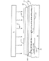
次に、図5を参照すると、ウェハW全体での放射10の不均一性、またはデバイス100の密度のばらつきが、ドーピングされたアモルファス領域30の温度に影響を与えている。図5では、ドーピングされたアモルファス領域30は、デバイス100のソース110Sおよびドレイン110Dである。これらのばらつきは位相切替層60の温度に影響を与えるだろう。この結果、ソース領域110Sおよびドレイン領域110Dが、1100℃〜1410℃の範囲にあるドーパント活性化温度範囲に達しないと、位相切替層60が活性化しない、すなわち、位相切替層60が位相を変えない。
【0031】
領域120内のデバイス100の密度は、領域130内のデバイスの密度よりも低いので、領域120は領域130と比較すると熱質量が小さい。したがって、入射放射線が均一である場合、領域120内のデバイス100は、領域130内のデバイスより早く加熱される。この結果、放射10で照射されると、領域120内のデバイス100は、領域130内のデバイスより先に活性化温度に達する。したがって、領域120の上にある位相切替層60の部分150は、第1の位相から第2の位相に遷移し、加熱することなく入射放射線10を吸収する。一方、領域130内のデバイス100は、活性化温度に達するまでの時間がより長く、吸収層50から熱を吸収し続ける。したがって、領域130上の位相切替層60の部分160は、第1の位相のままである時間がより長く、領域130内のデバイス100が活性化温度に達すると第2の位相に遷移する。領域120と130とが異なる反射性を有する場合でも同じ現象が生じる。
【0032】
位相切替層60の性質に適応性があるため、ウェハW上で、異なる熱質量または異なる反射性を有する領域(例えば領域120と130)を暴露しすぎることは困難である。したがって、デバイス構成の中でより多い量のレーザ放射またはより少ない量のレーザ放射を必要とする局所的な場所を、容易にまた自動的に補償することができる。
【0033】
(半導体デバイスを形成する方法)
上記に基づいて、本発明は、半導体ウェハ上に半導体デバイスを形成する方法を含む。再び図5を参照すると、この方法は、各々が活性化温度を有するソース領域110Sおよびドレイン領域110Dなどの、ドーピングされたアモルファスシリコン領域を有するデバイス100を含む1つまたは複数の加工領域を、半導体ウェハW内に形成するステップを含む。次のステップは、加工領域上に吸収層を堆積させ、吸収層の上または可能であれば吸収層の下に位相切替層を堆積させ、位相切替層が吸収層の上にある場合は位相切替層を介して吸収層を照射して吸収層および位相切替層を加熱することを含む。これらのステップは、位相切替層が活性化温度に達するまで吸収層からの熱で加工領域を加熱するステップとして上述されている。位相切替層が活性化温度に達すると、位相切替層は第1の位相(例えば、固体)から第2の位相(例えば、液体または気体)に切り替わるが、その間、温度を大幅に変えることなく熱を吸収して、吸収層の温度上昇を防ぐ。最終ステップは、吸収層および位相切替層を除去することである。よく知られたエッチング技術を使用して除去することができる。
【0034】
本発明を好ましい実施形態を用いて説明したが、本発明はこのように限定されるものではないことを理解されたい。逆に、付随する請求項に定義されたように、本発明の趣旨および範囲内に含まれるであろう、すべての代替例、修正例、および均等物をカバーすることが目的である。
【図面の簡単な説明】
【図1】
放射源に対してウェハホルダ内に配置された、ドーピングされたアモルファス領域を有する半導体ウェハ上に配置されたフィルムスタックの一部として示された、本発明の位相切替の模式的な断面図である。
【図2】
図1と同様な図であるが、フィルムスタックの位相切替層が、吸収層に隣接する、二酸化珪素からなる層と、前記二酸化珪素層に隣接する、アモルファスシリコンまたは多結晶シリコンとを含む。
【図3】
図1と同様な図であるが、位相切替層が、吸収層と、剥離を容易にする随意の層との間に挟まれ、放射エネルギー源は、狭く焦点を絞った放射ビームであり、ウェハ全体を走査して、基板上の任意のポイント(またはライン)で、時間的に短いエネルギーパルスを生成する図である。
【図4】
位相切替層の位相遷移層の温度(T64)に関して温度T対時間をプロットし、ドーピングされたアモルファス領域の温度(T30)対時間をプロットした図であり、加工領域が活性化される活性化温度(TA)またはその温度付近で、切替層の位相が、第1の位相から第2の位相に遷移する位相遷移温度TPを示す図である。
【図5】
デバイス密度が高い領域およびデバイス密度が低い領域にデバイス(例えばトランジスタ)を有し、図1のフィルムスタックが上に配置されたウェハを模式的に示す断面図である。
Claims (38)
- ワークピースの加工領域において、放射パルスに暴露されることから生じる最高温度を制御する熱誘導位相切替装置であって、
a)前記ワークピースの上に形成され、一部が前記加工領域をカバーし、放射線を吸収し、前記吸収した放射線を熱に変換する吸収層と、
b)前記吸収層に隣接して形成されるか密接して形成された位相切替層であって、前記位相切替層のうち前記加工領域をカバーする一部が、前記加工領域の望ましい最高温度に相当する位相変化温度を有し、位相遷移温度で位相が第1の位相から第2の位相に変化することで、前記加工領域における温度の上昇を限定する位相切替層とを備える、位相切替装置。 - 前記加工領域は活性化温度を有し、前記ワークピースは最高許容温度を有し、
前記位相遷移温度は、前記加工領域温度が前記活性化温度に達するが、前記ワークピースの最高許容温度を超えない温度である、請求項1に記載の装置。 - 前記吸収層と前記ワークピースの間に配置されるか、または、前記位相切替層と前記ワークピースとの間に配置される剥離可能層をさらに含む、請求項1に記載の装置。
- 前記加工領域はトランジスタのソース領域およびドレイン領域を含む、請求項1に記載の装置。
- 前記加工領域はドーピングされたアモルファスシリコンを含む、請求項1に記載の装置。
- 前記加工領域はドーピングされたアモルファスシリコンを含む、請求項2に記載の装置。
- 前記活性化温度は1100℃と1410℃の間である、請求項6に記載の装置。
- 前記吸収層は、チタン、タングステン、タンタル、酸化珪素、窒化珪素、窒化チタンのうち少なくとも1つを含む、請求項1に記載の装置。
- 前記位相切替層は、前記吸収層に隣接し、二酸化珪素からなる第1の層と、前記二酸化珪素からなる層に隣接し、ポリイミドまたはアルミニウム砒素からなる第2の層とを含む、請求項1に記載の装置。
- 前記位相切替層は、ポリイミドまたはアルミニウム砒素を含む、請求項1に記載の装置。
- 前記二酸化珪素からなる第1の層は、10と250nmとの間の厚さを有し、前記第2の層は、10nmと20ミクロンとの間の厚さを有するポリイミドである、請求項9に記載の装置。
- 前記二酸化珪素からなる第1の層は、10nmと250nmとの間の厚さを有し、前記第2の層は、10nmと20ミクロンとの間の厚さを有するアルミニウム砒素である、請求項9に記載の装置。
- 前記位相切替層の前記第1の位相は固体であり、前記第2の位相は気体または液体である、請求項1に記載の装置。
- 前記位相遷移温度は前記活性化温度より高い、請求項2に記載の装置。
- 前記位相遷移温度は前記活性化温度より低い、請求項2に記載の装置。
- ワークピースの加工領域で発生する最高温度を限定するシステムであって、
a)基板に渡って走査できる放射のパルスビームを提供することができる放射源と、
b)光源に隣接して配置され、前記ワークピースを支持するワークピースの支持部材と、
c)前記ワークピース上に配置された請求項1記載の熱誘導位相切替装置と、
を備える、システム。 - 前記放射のビームは、ラインまたはスポットを形成する、請求項16に記載のシステム。
- 前記放射源は、300nmと1100nmとの間の波長のレーザ放射を使用する、請求項16に記載の装置。
- ワークピースの加工領域に伝わる熱の量を制御する方法であって、前記加工領域は活性化温度を有し、
a)加工領域の上に吸収層を堆積させるステップと、
b)前記活性化温度に相当する位相遷移温度で第1の位相から第2の位相に位相を切り替えることができる位相切替層を、前記吸収層に近接して堆積させるステップと、
c)前記吸収層に照射して、前記吸収層および近接する前記位相切替層を加熱するステップと、
d)前記位相切替層が前記第1の位相から前記第2の位相に切り替わるまで、前記吸収層からの熱で前記加工領域を加熱して、前記吸収層に入射する放射線の吸収による温度の上昇を限定するステップと、
を含む方法。 - 前記加工領域はドーピングされたアモルファス領域であり、前記ステップd)は、前記加工領域を前記活性化温度に加熱することを含む、請求項19に記載の方法。
- 前記位相遷移温度は前記活性化温度より高い、請求項19に記載の方法。
- 前記位相遷移温度は前記活性化温度より低く、前記位相切替層は前記吸収層の上にある、請求項19に記載の方法。
- 前記ワークピースは、融解温度を有する結晶シリコンウェハであり、前記加工領域はドーピングされたアモルファスシリコンであり、
前記ステップd)は、前記加工領域を、前記活性化温度であるが前記結晶シリコンの融解温度よりも低い温度に加熱することを含む、請求項19に記載の方法。 - 前記照射ステップc)はパルスレーザ光を使用して行われる、請求項19に記載の方法。
- 前記照射ステップc)は、
i)狭いラインの放射線を形成し、
ii)前記基板に渡って前記放射ラインを走査することによって行われる、請求項19に記載の方法。 - 前記ステップb)は、前記吸収層の上に断熱層を形成すること、および前記断熱層の上に位相遷移層を形成することを含む、請求項19に記載の方法。
- 前記ステップb)は、前記吸収層の下に位相遷移層を形成することを含む、請求項19に記載の方法。
- 前記断熱層は二酸化珪素であり、前記位相遷移層はポリイミドおよびアルミニウム砒素のうち1つである、請求項26に記載の方法。
- 前記位相遷移層はポリイミドおよびアルミニウム砒素のうち1つである、請求項26に記載の方法。
- 前記加工領域が所与の放射エネルギーのパルスに関して望ましい温度に達すると、前記位相遷移層における位相遷移をトリガするように、前記断熱層の厚さを調節するステップをさらに含む、請求項26に記載の方法。
- 前記ステップb)は、前記吸収層の上に透過性位相シフト層を設置することと、基板上の層のスタックからの放射エネルギーの反射を最少にする厚さの前記透過性位相シフト層を選択することとを含む、請求項19に記載の方法。
- 前記位相シフト層の前記第1の位相は固体であり、前記第2の位相は液体または気体である、請求項19に記載の方法。
- 半導体ウェハから半導体デバイスを形成する方法であって、
a)活性化温度を有するドーピングされたアモルファスシリコンを含む加工領域を、半導体ウェハ内に形成するステップと、
b)加工領域上に吸収層を堆積させるステップと、
c)前記活性化温度に相当する位相遷移温度で、第1の位相から第2の位相反射状態に切り替えることができる位相切替層を、前記吸収層の上に堆積させるステップと、
d)前記位相切替層を介して前記吸収層に照射して、前記吸収層および前記位相切替層を加熱するステップと、
e)前記加工領域が前記活性化温度に達し、前記位相切替層が位相の変化を開始するまで、前記吸収層からの熱で前記加工領域を加熱して、前記基板の最高温度を限定するステップと、
f)前記吸収層および前記位相切替層を除去するステップと、
を含む方法。 - 前記ステップc)は、前記吸収層の上に断熱層を形成すること、および前記断熱層の上に位相遷移層を形成することを含む、請求項33に記載の方法。
- 前記ステップc)は、2層以上の断熱層を形成することを含む、請求項33に記載の方法。
- 前記ステップd)は、前記位相シフト層の第1の位相が固体であり、前記位相シフト層の第2の位相が液体または気体であるように前記位相シフト層を設計するステップを含む、請求項33に記載の方法。
- 半導体ウェハから半導体デバイスを形成する方法であって、
a)活性化温度を有するドーピングされたアモルファスシリコンを含む加工領域を、半導体ウェハ内に形成するステップと、
b)前記活性化温度に相当する位相遷移温度で第1の位相から第2の位相反射状態に切り替えることのできる位相切替層を、前記ドーピングされたアモルファスシリコン層の上に堆積させるステップと、
c)前記加工領域上に吸収層を堆積させるステップと、
d)前記位相切替層を介して前記吸収層を照射して、前記吸収層および前記位相切替層を加熱するステップと、
e)前記加工領域が前記活性化温度に達し前記位相切替層が位相を変え始めるまで、前記位相切替層からの熱で前記加工領域を加熱して、基板の最高温度を限定するステップと、
f)前記吸収層および前記位相切替層を除去するステップと、
を含む方法。 - 前記第1の位相は固体であり、前記第2の位相は液体または気体である、請求項37に記載の方法。
Applications Claiming Priority (3)
| Application Number | Priority Date | Filing Date | Title |
|---|---|---|---|
| US09/659,094 | 2000-09-11 | ||
| US09/659,094 US6479821B1 (en) | 2000-09-11 | 2000-09-11 | Thermally induced phase switch for laser thermal processing |
| PCT/US2001/042075 WO2002023279A1 (en) | 2000-09-11 | 2001-09-07 | Thermally induced phase switch for laser thermal processing |
Publications (2)
| Publication Number | Publication Date |
|---|---|
| JP2004509472A true JP2004509472A (ja) | 2004-03-25 |
| JP5273894B2 JP5273894B2 (ja) | 2013-08-28 |
Family
ID=24643989
Family Applications (1)
| Application Number | Title | Priority Date | Filing Date |
|---|---|---|---|
| JP2002527866A Expired - Fee Related JP5273894B2 (ja) | 2000-09-11 | 2001-09-07 | レーザ熱加工用の熱誘導位相切替 |
Country Status (3)
| Country | Link |
|---|---|
| US (1) | US6479821B1 (ja) |
| JP (1) | JP5273894B2 (ja) |
| WO (1) | WO2002023279A1 (ja) |
Cited By (1)
| Publication number | Priority date | Publication date | Assignee | Title |
|---|---|---|---|---|
| JP2007115926A (ja) * | 2005-10-20 | 2007-05-10 | Tokyo Univ Of Agriculture & Technology | サーマルヘッドおよび熱処理装置 |
Families Citing this family (245)
| Publication number | Priority date | Publication date | Assignee | Title |
|---|---|---|---|---|
| US6573030B1 (en) | 2000-02-17 | 2003-06-03 | Applied Materials, Inc. | Method for depositing an amorphous carbon layer |
| AU2004203186B2 (en) * | 2001-02-06 | 2005-07-14 | Zamtec Limited | A method of fabricating a printhead with nozzle protection |
| AUPR292301A0 (en) * | 2001-02-06 | 2001-03-01 | Silverbrook Research Pty. Ltd. | A method and apparatus (ART99) |
| US6844250B1 (en) | 2003-03-13 | 2005-01-18 | Ultratech, Inc. | Method and system for laser thermal processing of semiconductor devices |
| US7109087B2 (en) * | 2003-10-03 | 2006-09-19 | Applied Materials, Inc. | Absorber layer for DSA processing |
| KR101254107B1 (ko) * | 2003-10-03 | 2013-04-12 | 어플라이드 머티어리얼스, 인코포레이티드 | 다이나믹 표면 어닐링 프로세싱을 위한 흡수층 |
| US7145104B2 (en) * | 2004-02-26 | 2006-12-05 | Ultratech, Inc. | Silicon layer for uniformizing temperature during photo-annealing |
| US20070212859A1 (en) | 2006-03-08 | 2007-09-13 | Paul Carey | Method of thermal processing structures formed on a substrate |
| US7548364B2 (en) | 2006-07-31 | 2009-06-16 | Applied Materials, Inc. | Ultra-fast beam dithering with surface acoustic wave modulator |
| US20080025354A1 (en) * | 2006-07-31 | 2008-01-31 | Dean Jennings | Ultra-Fast Beam Dithering with Surface Acoustic Wave Modulator |
| US8148663B2 (en) | 2007-07-31 | 2012-04-03 | Applied Materials, Inc. | Apparatus and method of improving beam shaping and beam homogenization |
| US8427200B2 (en) | 2009-04-14 | 2013-04-23 | Monolithic 3D Inc. | 3D semiconductor device |
| US8362800B2 (en) | 2010-10-13 | 2013-01-29 | Monolithic 3D Inc. | 3D semiconductor device including field repairable logics |
| US7986042B2 (en) | 2009-04-14 | 2011-07-26 | Monolithic 3D Inc. | Method for fabrication of a semiconductor device and structure |
| US9509313B2 (en) | 2009-04-14 | 2016-11-29 | Monolithic 3D Inc. | 3D semiconductor device |
| US8373439B2 (en) | 2009-04-14 | 2013-02-12 | Monolithic 3D Inc. | 3D semiconductor device |
| US8362482B2 (en) | 2009-04-14 | 2013-01-29 | Monolithic 3D Inc. | Semiconductor device and structure |
| US8378715B2 (en) | 2009-04-14 | 2013-02-19 | Monolithic 3D Inc. | Method to construct systems |
| US8405420B2 (en) | 2009-04-14 | 2013-03-26 | Monolithic 3D Inc. | System comprising a semiconductor device and structure |
| US9577642B2 (en) | 2009-04-14 | 2017-02-21 | Monolithic 3D Inc. | Method to form a 3D semiconductor device |
| US8058137B1 (en) | 2009-04-14 | 2011-11-15 | Monolithic 3D Inc. | Method for fabrication of a semiconductor device and structure |
| US9711407B2 (en) | 2009-04-14 | 2017-07-18 | Monolithic 3D Inc. | Method of manufacturing a three dimensional integrated circuit by transfer of a mono-crystalline layer |
| US8384426B2 (en) | 2009-04-14 | 2013-02-26 | Monolithic 3D Inc. | Semiconductor device and structure |
| US8754533B2 (en) | 2009-04-14 | 2014-06-17 | Monolithic 3D Inc. | Monolithic three-dimensional semiconductor device and structure |
| US8669778B1 (en) | 2009-04-14 | 2014-03-11 | Monolithic 3D Inc. | Method for design and manufacturing of a 3D semiconductor device |
| US8395191B2 (en) | 2009-10-12 | 2013-03-12 | Monolithic 3D Inc. | Semiconductor device and structure |
| US10388863B2 (en) | 2009-10-12 | 2019-08-20 | Monolithic 3D Inc. | 3D memory device and structure |
| US10043781B2 (en) | 2009-10-12 | 2018-08-07 | Monolithic 3D Inc. | 3D semiconductor device and structure |
| US9099424B1 (en) | 2012-08-10 | 2015-08-04 | Monolithic 3D Inc. | Semiconductor system, device and structure with heat removal |
| US11984445B2 (en) | 2009-10-12 | 2024-05-14 | Monolithic 3D Inc. | 3D semiconductor devices and structures with metal layers |
| US8476145B2 (en) | 2010-10-13 | 2013-07-02 | Monolithic 3D Inc. | Method of fabricating a semiconductor device and structure |
| US11018133B2 (en) | 2009-10-12 | 2021-05-25 | Monolithic 3D Inc. | 3D integrated circuit |
| US10157909B2 (en) | 2009-10-12 | 2018-12-18 | Monolithic 3D Inc. | 3D semiconductor device and structure |
| US8581349B1 (en) | 2011-05-02 | 2013-11-12 | Monolithic 3D Inc. | 3D memory semiconductor device and structure |
| US10910364B2 (en) | 2009-10-12 | 2021-02-02 | Monolitaic 3D Inc. | 3D semiconductor device |
| US8742476B1 (en) | 2012-11-27 | 2014-06-03 | Monolithic 3D Inc. | Semiconductor device and structure |
| US8450804B2 (en) | 2011-03-06 | 2013-05-28 | Monolithic 3D Inc. | Semiconductor device and structure for heat removal |
| US12027518B1 (en) | 2009-10-12 | 2024-07-02 | Monolithic 3D Inc. | 3D semiconductor devices and structures with metal layers |
| US11374118B2 (en) | 2009-10-12 | 2022-06-28 | Monolithic 3D Inc. | Method to form a 3D integrated circuit |
| US10354995B2 (en) | 2009-10-12 | 2019-07-16 | Monolithic 3D Inc. | Semiconductor memory device and structure |
| US8294159B2 (en) | 2009-10-12 | 2012-10-23 | Monolithic 3D Inc. | Method for fabrication of a semiconductor device and structure |
| US10366970B2 (en) | 2009-10-12 | 2019-07-30 | Monolithic 3D Inc. | 3D semiconductor device and structure |
| US8536023B2 (en) | 2010-11-22 | 2013-09-17 | Monolithic 3D Inc. | Method of manufacturing a semiconductor device and structure |
| US8026521B1 (en) | 2010-10-11 | 2011-09-27 | Monolithic 3D Inc. | Semiconductor device and structure |
| US8492886B2 (en) | 2010-02-16 | 2013-07-23 | Monolithic 3D Inc | 3D integrated circuit with logic |
| US8373230B1 (en) | 2010-10-13 | 2013-02-12 | Monolithic 3D Inc. | Method for fabrication of a semiconductor device and structure |
| US8541819B1 (en) | 2010-12-09 | 2013-09-24 | Monolithic 3D Inc. | Semiconductor device and structure |
| US9099526B2 (en) | 2010-02-16 | 2015-08-04 | Monolithic 3D Inc. | Integrated circuit device and structure |
| US8461035B1 (en) | 2010-09-30 | 2013-06-11 | Monolithic 3D Inc. | Method for fabrication of a semiconductor device and structure |
| US8901613B2 (en) | 2011-03-06 | 2014-12-02 | Monolithic 3D Inc. | Semiconductor device and structure for heat removal |
| US10217667B2 (en) | 2011-06-28 | 2019-02-26 | Monolithic 3D Inc. | 3D semiconductor device, fabrication method and system |
| US9219005B2 (en) | 2011-06-28 | 2015-12-22 | Monolithic 3D Inc. | Semiconductor system and device |
| US8642416B2 (en) | 2010-07-30 | 2014-02-04 | Monolithic 3D Inc. | Method of forming three dimensional integrated circuit devices using layer transfer technique |
| US9953925B2 (en) | 2011-06-28 | 2018-04-24 | Monolithic 3D Inc. | Semiconductor system and device |
| US8273610B2 (en) | 2010-11-18 | 2012-09-25 | Monolithic 3D Inc. | Method of constructing a semiconductor device and structure |
| US10497713B2 (en) | 2010-11-18 | 2019-12-03 | Monolithic 3D Inc. | 3D semiconductor memory device and structure |
| US12362219B2 (en) | 2010-11-18 | 2025-07-15 | Monolithic 3D Inc. | 3D semiconductor memory device and structure |
| US11482440B2 (en) | 2010-12-16 | 2022-10-25 | Monolithic 3D Inc. | 3D semiconductor device and structure with a built-in test circuit for repairing faulty circuits |
| US8163581B1 (en) | 2010-10-13 | 2012-04-24 | Monolith IC 3D | Semiconductor and optoelectronic devices |
| US8114757B1 (en) | 2010-10-11 | 2012-02-14 | Monolithic 3D Inc. | Semiconductor device and structure |
| US11600667B1 (en) | 2010-10-11 | 2023-03-07 | Monolithic 3D Inc. | Method to produce 3D semiconductor devices and structures with memory |
| US10290682B2 (en) | 2010-10-11 | 2019-05-14 | Monolithic 3D Inc. | 3D IC semiconductor device and structure with stacked memory |
| US11018191B1 (en) | 2010-10-11 | 2021-05-25 | Monolithic 3D Inc. | 3D semiconductor device and structure |
| US11315980B1 (en) | 2010-10-11 | 2022-04-26 | Monolithic 3D Inc. | 3D semiconductor device and structure with transistors |
| US11257867B1 (en) | 2010-10-11 | 2022-02-22 | Monolithic 3D Inc. | 3D semiconductor device and structure with oxide bonds |
| US10896931B1 (en) | 2010-10-11 | 2021-01-19 | Monolithic 3D Inc. | 3D semiconductor device and structure |
| US11158674B2 (en) | 2010-10-11 | 2021-10-26 | Monolithic 3D Inc. | Method to produce a 3D semiconductor device and structure |
| US11469271B2 (en) | 2010-10-11 | 2022-10-11 | Monolithic 3D Inc. | Method to produce 3D semiconductor devices and structures with memory |
| US11024673B1 (en) | 2010-10-11 | 2021-06-01 | Monolithic 3D Inc. | 3D semiconductor device and structure |
| US11227897B2 (en) | 2010-10-11 | 2022-01-18 | Monolithic 3D Inc. | Method for producing a 3D semiconductor memory device and structure |
| US12360310B2 (en) | 2010-10-13 | 2025-07-15 | Monolithic 3D Inc. | Multilevel semiconductor device and structure with oxide bonding |
| US11869915B2 (en) | 2010-10-13 | 2024-01-09 | Monolithic 3D Inc. | Multilevel semiconductor device and structure with image sensors and wafer bonding |
| US9197804B1 (en) | 2011-10-14 | 2015-11-24 | Monolithic 3D Inc. | Semiconductor and optoelectronic devices |
| US11855114B2 (en) | 2010-10-13 | 2023-12-26 | Monolithic 3D Inc. | Multilevel semiconductor device and structure with image sensors and wafer bonding |
| US12080743B2 (en) | 2010-10-13 | 2024-09-03 | Monolithic 3D Inc. | Multilevel semiconductor device and structure with image sensors and wafer bonding |
| US11984438B2 (en) | 2010-10-13 | 2024-05-14 | Monolithic 3D Inc. | Multilevel semiconductor device and structure with oxide bonding |
| US11163112B2 (en) | 2010-10-13 | 2021-11-02 | Monolithic 3D Inc. | Multilevel semiconductor device and structure with electromagnetic modulators |
| US10679977B2 (en) | 2010-10-13 | 2020-06-09 | Monolithic 3D Inc. | 3D microdisplay device and structure |
| US10943934B2 (en) | 2010-10-13 | 2021-03-09 | Monolithic 3D Inc. | Multilevel semiconductor device and structure |
| US11063071B1 (en) | 2010-10-13 | 2021-07-13 | Monolithic 3D Inc. | Multilevel semiconductor device and structure with waveguides |
| US11327227B2 (en) | 2010-10-13 | 2022-05-10 | Monolithic 3D Inc. | Multilevel semiconductor device and structure with electromagnetic modulators |
| US11437368B2 (en) | 2010-10-13 | 2022-09-06 | Monolithic 3D Inc. | Multilevel semiconductor device and structure with oxide bonding |
| US11694922B2 (en) | 2010-10-13 | 2023-07-04 | Monolithic 3D Inc. | Multilevel semiconductor device and structure with oxide bonding |
| US11043523B1 (en) | 2010-10-13 | 2021-06-22 | Monolithic 3D Inc. | Multilevel semiconductor device and structure with image sensors |
| US10978501B1 (en) | 2010-10-13 | 2021-04-13 | Monolithic 3D Inc. | Multilevel semiconductor device and structure with waveguides |
| US11605663B2 (en) | 2010-10-13 | 2023-03-14 | Monolithic 3D Inc. | Multilevel semiconductor device and structure with image sensors and wafer bonding |
| US11855100B2 (en) | 2010-10-13 | 2023-12-26 | Monolithic 3D Inc. | Multilevel semiconductor device and structure with oxide bonding |
| US11929372B2 (en) | 2010-10-13 | 2024-03-12 | Monolithic 3D Inc. | Multilevel semiconductor device and structure with image sensors and wafer bonding |
| US10998374B1 (en) | 2010-10-13 | 2021-05-04 | Monolithic 3D Inc. | Multilevel semiconductor device and structure |
| US10833108B2 (en) | 2010-10-13 | 2020-11-10 | Monolithic 3D Inc. | 3D microdisplay device and structure |
| US11164898B2 (en) | 2010-10-13 | 2021-11-02 | Monolithic 3D Inc. | Multilevel semiconductor device and structure |
| US8379458B1 (en) | 2010-10-13 | 2013-02-19 | Monolithic 3D Inc. | Semiconductor device and structure |
| US11404466B2 (en) | 2010-10-13 | 2022-08-02 | Monolithic 3D Inc. | Multilevel semiconductor device and structure with image sensors |
| US12094892B2 (en) | 2010-10-13 | 2024-09-17 | Monolithic 3D Inc. | 3D micro display device and structure |
| US11133344B2 (en) | 2010-10-13 | 2021-09-28 | Monolithic 3D Inc. | Multilevel semiconductor device and structure with image sensors |
| US8026519B1 (en) | 2010-10-22 | 2011-09-27 | Ultratech, Inc. | Systems and methods for forming a time-averaged line image |
| US8399808B2 (en) | 2010-10-22 | 2013-03-19 | Ultratech, Inc. | Systems and methods for forming a time-averaged line image |
| US11004719B1 (en) | 2010-11-18 | 2021-05-11 | Monolithic 3D Inc. | Methods for producing a 3D semiconductor memory device and structure |
| US11121021B2 (en) | 2010-11-18 | 2021-09-14 | Monolithic 3D Inc. | 3D semiconductor device and structure |
| US12136562B2 (en) | 2010-11-18 | 2024-11-05 | Monolithic 3D Inc. | 3D semiconductor device and structure with single-crystal layers |
| US11482439B2 (en) | 2010-11-18 | 2022-10-25 | Monolithic 3D Inc. | Methods for producing a 3D semiconductor memory device comprising charge trap junction-less transistors |
| US11107721B2 (en) | 2010-11-18 | 2021-08-31 | Monolithic 3D Inc. | 3D semiconductor device and structure with NAND logic |
| US11355381B2 (en) | 2010-11-18 | 2022-06-07 | Monolithic 3D Inc. | 3D semiconductor memory device and structure |
| US11615977B2 (en) | 2010-11-18 | 2023-03-28 | Monolithic 3D Inc. | 3D semiconductor memory device and structure |
| US11610802B2 (en) | 2010-11-18 | 2023-03-21 | Monolithic 3D Inc. | Method for producing a 3D semiconductor device and structure with single crystal transistors and metal gate electrodes |
| US11018042B1 (en) | 2010-11-18 | 2021-05-25 | Monolithic 3D Inc. | 3D semiconductor memory device and structure |
| US11094576B1 (en) | 2010-11-18 | 2021-08-17 | Monolithic 3D Inc. | Methods for producing a 3D semiconductor memory device and structure |
| US12243765B2 (en) | 2010-11-18 | 2025-03-04 | Monolithic 3D Inc. | 3D semiconductor device and structure with metal layers and memory cells |
| US11804396B2 (en) | 2010-11-18 | 2023-10-31 | Monolithic 3D Inc. | Methods for producing a 3D semiconductor device and structure with memory cells and multiple metal layers |
| US12272586B2 (en) | 2010-11-18 | 2025-04-08 | Monolithic 3D Inc. | 3D semiconductor memory device and structure with memory and metal layers |
| US11164770B1 (en) | 2010-11-18 | 2021-11-02 | Monolithic 3D Inc. | Method for producing a 3D semiconductor memory device and structure |
| US11443971B2 (en) | 2010-11-18 | 2022-09-13 | Monolithic 3D Inc. | 3D semiconductor device and structure with memory |
| US11854857B1 (en) | 2010-11-18 | 2023-12-26 | Monolithic 3D Inc. | Methods for producing a 3D semiconductor device and structure with memory cells and multiple metal layers |
| US11862503B2 (en) | 2010-11-18 | 2024-01-02 | Monolithic 3D Inc. | Method for producing a 3D semiconductor device and structure with memory cells and multiple metal layers |
| US11482438B2 (en) | 2010-11-18 | 2022-10-25 | Monolithic 3D Inc. | Methods for producing a 3D semiconductor memory device and structure |
| US11923230B1 (en) | 2010-11-18 | 2024-03-05 | Monolithic 3D Inc. | 3D semiconductor device and structure with bonding |
| US12154817B1 (en) | 2010-11-18 | 2024-11-26 | Monolithic 3D Inc. | Methods for producing a 3D semiconductor memory device and structure |
| US11355380B2 (en) | 2010-11-18 | 2022-06-07 | Monolithic 3D Inc. | Methods for producing 3D semiconductor memory device and structure utilizing alignment marks |
| US12125737B1 (en) | 2010-11-18 | 2024-10-22 | Monolithic 3D Inc. | 3D semiconductor device and structure with metal layers and memory cells |
| US11521888B2 (en) | 2010-11-18 | 2022-12-06 | Monolithic 3D Inc. | 3D semiconductor device and structure with high-k metal gate transistors |
| US12033884B2 (en) | 2010-11-18 | 2024-07-09 | Monolithic 3D Inc. | Methods for producing a 3D semiconductor device and structure with memory cells and multiple metal layers |
| US12100611B2 (en) | 2010-11-18 | 2024-09-24 | Monolithic 3D Inc. | Methods for producing a 3D semiconductor device and structure with memory cells and multiple metal layers |
| US12144190B2 (en) | 2010-11-18 | 2024-11-12 | Monolithic 3D Inc. | 3D semiconductor device and structure with bonding and memory cells preliminary class |
| US11569117B2 (en) | 2010-11-18 | 2023-01-31 | Monolithic 3D Inc. | 3D semiconductor device and structure with single-crystal layers |
| US11211279B2 (en) | 2010-11-18 | 2021-12-28 | Monolithic 3D Inc. | Method for processing a 3D integrated circuit and structure |
| US12068187B2 (en) | 2010-11-18 | 2024-08-20 | Monolithic 3D Inc. | 3D semiconductor device and structure with bonding and DRAM memory cells |
| US11508605B2 (en) | 2010-11-18 | 2022-11-22 | Monolithic 3D Inc. | 3D semiconductor memory device and structure |
| US11784082B2 (en) | 2010-11-18 | 2023-10-10 | Monolithic 3D Inc. | 3D semiconductor device and structure with bonding |
| US11031275B2 (en) | 2010-11-18 | 2021-06-08 | Monolithic 3D Inc. | 3D semiconductor device and structure with memory |
| US11495484B2 (en) | 2010-11-18 | 2022-11-08 | Monolithic 3D Inc. | 3D semiconductor devices and structures with at least two single-crystal layers |
| US11735462B2 (en) | 2010-11-18 | 2023-08-22 | Monolithic 3D Inc. | 3D semiconductor device and structure with single-crystal layers |
| US11901210B2 (en) | 2010-11-18 | 2024-02-13 | Monolithic 3D Inc. | 3D semiconductor device and structure with memory |
| US12463076B2 (en) | 2010-12-16 | 2025-11-04 | Monolithic 3D Inc. | 3D semiconductor device and structure |
| US8975670B2 (en) | 2011-03-06 | 2015-03-10 | Monolithic 3D Inc. | Semiconductor device and structure for heat removal |
| US8309474B1 (en) | 2011-06-07 | 2012-11-13 | Ultratech, Inc. | Ultrafast laser annealing with reduced pattern density effects in integrated circuit fabrication |
| US9302348B2 (en) | 2011-06-07 | 2016-04-05 | Ultratech Inc. | Ultrafast laser annealing with reduced pattern density effects in integrated circuit fabrication |
| US10388568B2 (en) | 2011-06-28 | 2019-08-20 | Monolithic 3D Inc. | 3D semiconductor device and system |
| US8687399B2 (en) | 2011-10-02 | 2014-04-01 | Monolithic 3D Inc. | Semiconductor device and structure |
| US9029173B2 (en) | 2011-10-18 | 2015-05-12 | Monolithic 3D Inc. | Method for fabrication of a semiconductor device and structure |
| US8546805B2 (en) | 2012-01-27 | 2013-10-01 | Ultratech, Inc. | Two-beam laser annealing with improved temperature performance |
| US9000557B2 (en) | 2012-03-17 | 2015-04-07 | Zvi Or-Bach | Semiconductor device and structure |
| US11164811B2 (en) | 2012-04-09 | 2021-11-02 | Monolithic 3D Inc. | 3D semiconductor device with isolation layers and oxide-to-oxide bonding |
| US11410912B2 (en) | 2012-04-09 | 2022-08-09 | Monolithic 3D Inc. | 3D semiconductor device with vias and isolation layers |
| US10600888B2 (en) | 2012-04-09 | 2020-03-24 | Monolithic 3D Inc. | 3D semiconductor device |
| US11616004B1 (en) | 2012-04-09 | 2023-03-28 | Monolithic 3D Inc. | 3D semiconductor device and structure with metal layers and a connective path |
| US11594473B2 (en) | 2012-04-09 | 2023-02-28 | Monolithic 3D Inc. | 3D semiconductor device and structure with metal layers and a connective path |
| US11476181B1 (en) | 2012-04-09 | 2022-10-18 | Monolithic 3D Inc. | 3D semiconductor device and structure with metal layers |
| US11735501B1 (en) | 2012-04-09 | 2023-08-22 | Monolithic 3D Inc. | 3D semiconductor device and structure with metal layers and a connective path |
| US11088050B2 (en) | 2012-04-09 | 2021-08-10 | Monolithic 3D Inc. | 3D semiconductor device with isolation layers |
| US11881443B2 (en) | 2012-04-09 | 2024-01-23 | Monolithic 3D Inc. | 3D semiconductor device and structure with metal layers and a connective path |
| US8557632B1 (en) | 2012-04-09 | 2013-10-15 | Monolithic 3D Inc. | Method for fabrication of a semiconductor device and structure |
| US11694944B1 (en) | 2012-04-09 | 2023-07-04 | Monolithic 3D Inc. | 3D semiconductor device and structure with metal layers and a connective path |
| US8501638B1 (en) | 2012-04-27 | 2013-08-06 | Ultratech, Inc. | Laser annealing scanning methods with reduced annealing non-uniformities |
| SG10201503478UA (en) | 2012-06-11 | 2015-06-29 | Ultratech Inc | Laser annealing systems and methods with ultra-short dwell times |
| US9558973B2 (en) | 2012-06-11 | 2017-01-31 | Ultratech, Inc. | Laser annealing systems and methods with ultra-short dwell times |
| US9490128B2 (en) | 2012-08-27 | 2016-11-08 | Ultratech, Inc. | Non-melt thin-wafer laser thermal annealing methods |
| CN102796995B (zh) * | 2012-08-27 | 2015-01-28 | 北京博宇半导体工艺器皿技术有限公司 | 制备热解氮化硼制品的气相沉积炉及方法 |
| US8574929B1 (en) | 2012-11-16 | 2013-11-05 | Monolithic 3D Inc. | Method to form a 3D semiconductor device and structure |
| US8686428B1 (en) | 2012-11-16 | 2014-04-01 | Monolithic 3D Inc. | Semiconductor device and structure |
| US8674470B1 (en) | 2012-12-22 | 2014-03-18 | Monolithic 3D Inc. | Semiconductor device and structure |
| US11967583B2 (en) | 2012-12-22 | 2024-04-23 | Monolithic 3D Inc. | 3D semiconductor device and structure with metal layers |
| US11063024B1 (en) | 2012-12-22 | 2021-07-13 | Monlithic 3D Inc. | Method to form a 3D semiconductor device and structure |
| US11217565B2 (en) | 2012-12-22 | 2022-01-04 | Monolithic 3D Inc. | Method to form a 3D semiconductor device and structure |
| US11784169B2 (en) | 2012-12-22 | 2023-10-10 | Monolithic 3D Inc. | 3D semiconductor device and structure with metal layers |
| US11961827B1 (en) | 2012-12-22 | 2024-04-16 | Monolithic 3D Inc. | 3D semiconductor device and structure with metal layers |
| US11309292B2 (en) | 2012-12-22 | 2022-04-19 | Monolithic 3D Inc. | 3D semiconductor device and structure with metal layers |
| US12051674B2 (en) | 2012-12-22 | 2024-07-30 | Monolithic 3D Inc. | 3D semiconductor device and structure with metal layers |
| US11916045B2 (en) | 2012-12-22 | 2024-02-27 | Monolithic 3D Inc. | 3D semiconductor device and structure with metal layers |
| US11018116B2 (en) | 2012-12-22 | 2021-05-25 | Monolithic 3D Inc. | Method to form a 3D semiconductor device and structure |
| US10903089B1 (en) | 2012-12-29 | 2021-01-26 | Monolithic 3D Inc. | 3D semiconductor device and structure |
| US11430667B2 (en) | 2012-12-29 | 2022-08-30 | Monolithic 3D Inc. | 3D semiconductor device and structure with bonding |
| US12249538B2 (en) | 2012-12-29 | 2025-03-11 | Monolithic 3D Inc. | 3D semiconductor device and structure including power distribution grids |
| US11430668B2 (en) | 2012-12-29 | 2022-08-30 | Monolithic 3D Inc. | 3D semiconductor device and structure with bonding |
| US11087995B1 (en) | 2012-12-29 | 2021-08-10 | Monolithic 3D Inc. | 3D semiconductor device and structure |
| US9871034B1 (en) | 2012-12-29 | 2018-01-16 | Monolithic 3D Inc. | Semiconductor device and structure |
| US10115663B2 (en) | 2012-12-29 | 2018-10-30 | Monolithic 3D Inc. | 3D semiconductor device and structure |
| US11177140B2 (en) | 2012-12-29 | 2021-11-16 | Monolithic 3D Inc. | 3D semiconductor device and structure |
| US11004694B1 (en) | 2012-12-29 | 2021-05-11 | Monolithic 3D Inc. | 3D semiconductor device and structure |
| US10651054B2 (en) | 2012-12-29 | 2020-05-12 | Monolithic 3D Inc. | 3D semiconductor device and structure |
| US10892169B2 (en) | 2012-12-29 | 2021-01-12 | Monolithic 3D Inc. | 3D semiconductor device and structure |
| US10600657B2 (en) | 2012-12-29 | 2020-03-24 | Monolithic 3D Inc | 3D semiconductor device and structure |
| US9385058B1 (en) | 2012-12-29 | 2016-07-05 | Monolithic 3D Inc. | Semiconductor device and structure |
| US8902663B1 (en) | 2013-03-11 | 2014-12-02 | Monolithic 3D Inc. | Method of maintaining a memory state |
| US12094965B2 (en) | 2013-03-11 | 2024-09-17 | Monolithic 3D Inc. | 3D semiconductor device and structure with metal layers and memory cells |
| US11935949B1 (en) | 2013-03-11 | 2024-03-19 | Monolithic 3D Inc. | 3D semiconductor device and structure with metal layers and memory cells |
| US10325651B2 (en) | 2013-03-11 | 2019-06-18 | Monolithic 3D Inc. | 3D semiconductor device with stacked memory |
| US11869965B2 (en) | 2013-03-11 | 2024-01-09 | Monolithic 3D Inc. | 3D semiconductor device and structure with metal layers and memory cells |
| US11398569B2 (en) | 2013-03-12 | 2022-07-26 | Monolithic 3D Inc. | 3D semiconductor device and structure |
| US10840239B2 (en) | 2014-08-26 | 2020-11-17 | Monolithic 3D Inc. | 3D semiconductor device and structure |
| US8994404B1 (en) | 2013-03-12 | 2015-03-31 | Monolithic 3D Inc. | Semiconductor device and structure |
| US11088130B2 (en) | 2014-01-28 | 2021-08-10 | Monolithic 3D Inc. | 3D semiconductor device and structure |
| US12100646B2 (en) | 2013-03-12 | 2024-09-24 | Monolithic 3D Inc. | 3D semiconductor device and structure with metal layers |
| US11923374B2 (en) | 2013-03-12 | 2024-03-05 | Monolithic 3D Inc. | 3D semiconductor device and structure with metal layers |
| US10224279B2 (en) | 2013-03-15 | 2019-03-05 | Monolithic 3D Inc. | Semiconductor device and structure |
| US9117749B1 (en) | 2013-03-15 | 2015-08-25 | Monolithic 3D Inc. | Semiconductor device and structure |
| US9021414B1 (en) | 2013-04-15 | 2015-04-28 | Monolithic 3D Inc. | Automation for monolithic 3D devices |
| US11030371B2 (en) | 2013-04-15 | 2021-06-08 | Monolithic 3D Inc. | Automation for monolithic 3D devices |
| US11341309B1 (en) | 2013-04-15 | 2022-05-24 | Monolithic 3D Inc. | Automation for monolithic 3D devices |
| US11487928B2 (en) | 2013-04-15 | 2022-11-01 | Monolithic 3D Inc. | Automation for monolithic 3D devices |
| US11720736B2 (en) | 2013-04-15 | 2023-08-08 | Monolithic 3D Inc. | Automation methods for 3D integrated circuits and devices |
| US11270055B1 (en) | 2013-04-15 | 2022-03-08 | Monolithic 3D Inc. | Automation for monolithic 3D devices |
| US11574109B1 (en) | 2013-04-15 | 2023-02-07 | Monolithic 3D Inc | Automation methods for 3D integrated circuits and devices |
| WO2015023791A1 (en) * | 2013-08-16 | 2015-02-19 | Applied Materials, Inc. | Dynamic optical valve for mitigating non-uniform heating in laser processing |
| US9343307B2 (en) | 2013-12-24 | 2016-05-17 | Ultratech, Inc. | Laser spike annealing using fiber lasers |
| US12094829B2 (en) | 2014-01-28 | 2024-09-17 | Monolithic 3D Inc. | 3D semiconductor device and structure |
| US10297586B2 (en) | 2015-03-09 | 2019-05-21 | Monolithic 3D Inc. | Methods for processing a 3D semiconductor device |
| US11107808B1 (en) | 2014-01-28 | 2021-08-31 | Monolithic 3D Inc. | 3D semiconductor device and structure |
| US11031394B1 (en) | 2014-01-28 | 2021-06-08 | Monolithic 3D Inc. | 3D semiconductor device and structure |
| JP6193305B2 (ja) | 2014-07-29 | 2017-09-06 | ウルトラテック インク | 高性能線形成光学システム及び方法 |
| US10083843B2 (en) | 2014-12-17 | 2018-09-25 | Ultratech, Inc. | Laser annealing systems and methods with ultra-short dwell times |
| US11056468B1 (en) | 2015-04-19 | 2021-07-06 | Monolithic 3D Inc. | 3D semiconductor device and structure |
| US12477752B2 (en) | 2015-09-21 | 2025-11-18 | Monolithic 3D Inc. | 3D semiconductor memory devices and structures |
| US11011507B1 (en) | 2015-04-19 | 2021-05-18 | Monolithic 3D Inc. | 3D semiconductor device and structure |
| US12035531B2 (en) | 2015-10-24 | 2024-07-09 | Monolithic 3D Inc. | 3D semiconductor device and structure with logic and memory |
| US11114427B2 (en) | 2015-11-07 | 2021-09-07 | Monolithic 3D Inc. | 3D semiconductor processor and memory device and structure |
| US12219769B2 (en) | 2015-10-24 | 2025-02-04 | Monolithic 3D Inc. | 3D semiconductor device and structure with logic and memory |
| US11937422B2 (en) | 2015-11-07 | 2024-03-19 | Monolithic 3D Inc. | Semiconductor memory device and structure |
| US10825779B2 (en) | 2015-04-19 | 2020-11-03 | Monolithic 3D Inc. | 3D semiconductor device and structure |
| US12016181B2 (en) | 2015-10-24 | 2024-06-18 | Monolithic 3D Inc. | 3D semiconductor device and structure with logic and memory |
| US11296115B1 (en) | 2015-10-24 | 2022-04-05 | Monolithic 3D Inc. | 3D semiconductor device and structure |
| US11978731B2 (en) | 2015-09-21 | 2024-05-07 | Monolithic 3D Inc. | Method to produce a multi-level semiconductor memory device and structure |
| US10418369B2 (en) | 2015-10-24 | 2019-09-17 | Monolithic 3D Inc. | Multi-level semiconductor memory device and structure |
| US10381328B2 (en) | 2015-04-19 | 2019-08-13 | Monolithic 3D Inc. | Semiconductor device and structure |
| US11114464B2 (en) | 2015-10-24 | 2021-09-07 | Monolithic 3D Inc. | 3D semiconductor device and structure |
| US10847540B2 (en) | 2015-10-24 | 2020-11-24 | Monolithic 3D Inc. | 3D semiconductor memory device and structure |
| US11956952B2 (en) | 2015-08-23 | 2024-04-09 | Monolithic 3D Inc. | Semiconductor memory device and structure |
| US12250830B2 (en) | 2015-09-21 | 2025-03-11 | Monolithic 3D Inc. | 3D semiconductor memory devices and structures |
| DE112016004265T5 (de) | 2015-09-21 | 2018-06-07 | Monolithic 3D Inc. | 3d halbleitervorrichtung und -struktur |
| US12100658B2 (en) | 2015-09-21 | 2024-09-24 | Monolithic 3D Inc. | Method to produce a 3D multilayer semiconductor device and structure |
| US12178055B2 (en) | 2015-09-21 | 2024-12-24 | Monolithic 3D Inc. | 3D semiconductor memory devices and structures |
| US10522225B1 (en) | 2015-10-02 | 2019-12-31 | Monolithic 3D Inc. | Semiconductor device with non-volatile memory |
| US12120880B1 (en) | 2015-10-24 | 2024-10-15 | Monolithic 3D Inc. | 3D semiconductor device and structure with logic and memory |
| US11991884B1 (en) | 2015-10-24 | 2024-05-21 | Monolithic 3D Inc. | 3D semiconductor device and structure with logic and memory |
| US11930648B1 (en) | 2016-10-10 | 2024-03-12 | Monolithic 3D Inc. | 3D memory devices and structures with metal layers |
| US11329059B1 (en) | 2016-10-10 | 2022-05-10 | Monolithic 3D Inc. | 3D memory devices and structures with thinned single crystal substrates |
| US11711928B2 (en) | 2016-10-10 | 2023-07-25 | Monolithic 3D Inc. | 3D memory devices and structures with control circuits |
| US11812620B2 (en) | 2016-10-10 | 2023-11-07 | Monolithic 3D Inc. | 3D DRAM memory devices and structures with control circuits |
| US11869591B2 (en) | 2016-10-10 | 2024-01-09 | Monolithic 3D Inc. | 3D memory devices and structures with control circuits |
| US12225704B2 (en) | 2016-10-10 | 2025-02-11 | Monolithic 3D Inc. | 3D memory devices and structures with memory arrays and metal layers |
| US11251149B2 (en) | 2016-10-10 | 2022-02-15 | Monolithic 3D Inc. | 3D memory device and structure |
| US11763864B2 (en) | 2019-04-08 | 2023-09-19 | Monolithic 3D Inc. | 3D memory semiconductor devices and structures with bit-line pillars |
| US11018156B2 (en) | 2019-04-08 | 2021-05-25 | Monolithic 3D Inc. | 3D memory semiconductor devices and structures |
| US11158652B1 (en) | 2019-04-08 | 2021-10-26 | Monolithic 3D Inc. | 3D memory semiconductor devices and structures |
| US10892016B1 (en) | 2019-04-08 | 2021-01-12 | Monolithic 3D Inc. | 3D memory semiconductor devices and structures |
| US11296106B2 (en) | 2019-04-08 | 2022-04-05 | Monolithic 3D Inc. | 3D memory semiconductor devices and structures |
Citations (6)
| Publication number | Priority date | Publication date | Assignee | Title |
|---|---|---|---|---|
| JPS59158515A (ja) * | 1983-02-28 | 1984-09-08 | Fujitsu Ltd | 半導体装置の製造方法 |
| JPS6448410A (en) * | 1987-08-19 | 1989-02-22 | Hitachi Ltd | Manufacture of semiconductor device |
| JPH04332120A (ja) * | 1991-05-07 | 1992-11-19 | Ricoh Co Ltd | 半導体結晶層の製造方法 |
| JPH08139016A (ja) * | 1994-11-07 | 1996-05-31 | Fuji Xerox Co Ltd | 薄膜集積回路の製造方法 |
| WO2000013213A1 (en) * | 1998-08-27 | 2000-03-09 | Ultratech Stepper, Inc. | Gas immersion laser annealing method suitable for use in the fabrication of reduced-dimension integrated circuits |
| JP2000138177A (ja) * | 1998-10-29 | 2000-05-16 | Sharp Corp | 半導体装置の製造方法 |
Family Cites Families (3)
| Publication number | Priority date | Publication date | Assignee | Title |
|---|---|---|---|---|
| US5908307A (en) | 1997-01-31 | 1999-06-01 | Ultratech Stepper, Inc. | Fabrication method for reduced-dimension FET devices |
| US6274488B1 (en) * | 2000-04-12 | 2001-08-14 | Ultratech Stepper, Inc. | Method of forming a silicide region in a Si substrate and a device having same |
| US6303476B1 (en) * | 2000-06-12 | 2001-10-16 | Ultratech Stepper, Inc. | Thermally induced reflectivity switch for laser thermal processing |
-
2000
- 2000-09-11 US US09/659,094 patent/US6479821B1/en not_active Expired - Lifetime
-
2001
- 2001-09-07 JP JP2002527866A patent/JP5273894B2/ja not_active Expired - Fee Related
- 2001-09-07 WO PCT/US2001/042075 patent/WO2002023279A1/en not_active Ceased
Patent Citations (7)
| Publication number | Priority date | Publication date | Assignee | Title |
|---|---|---|---|---|
| JPS59158515A (ja) * | 1983-02-28 | 1984-09-08 | Fujitsu Ltd | 半導体装置の製造方法 |
| JPS6448410A (en) * | 1987-08-19 | 1989-02-22 | Hitachi Ltd | Manufacture of semiconductor device |
| JPH04332120A (ja) * | 1991-05-07 | 1992-11-19 | Ricoh Co Ltd | 半導体結晶層の製造方法 |
| JPH08139016A (ja) * | 1994-11-07 | 1996-05-31 | Fuji Xerox Co Ltd | 薄膜集積回路の製造方法 |
| WO2000013213A1 (en) * | 1998-08-27 | 2000-03-09 | Ultratech Stepper, Inc. | Gas immersion laser annealing method suitable for use in the fabrication of reduced-dimension integrated circuits |
| JP2002524846A (ja) * | 1998-08-27 | 2002-08-06 | ウルトラテック ステッパー インコーポレイテッド | 小型集積回路の作製における用途に適したガス浸漬レーザアニーリング方法 |
| JP2000138177A (ja) * | 1998-10-29 | 2000-05-16 | Sharp Corp | 半導体装置の製造方法 |
Cited By (1)
| Publication number | Priority date | Publication date | Assignee | Title |
|---|---|---|---|---|
| JP2007115926A (ja) * | 2005-10-20 | 2007-05-10 | Tokyo Univ Of Agriculture & Technology | サーマルヘッドおよび熱処理装置 |
Also Published As
| Publication number | Publication date |
|---|---|
| US6479821B1 (en) | 2002-11-12 |
| JP5273894B2 (ja) | 2013-08-28 |
| WO2002023279A1 (en) | 2002-03-21 |
Similar Documents
| Publication | Publication Date | Title |
|---|---|---|
| JP5273894B2 (ja) | レーザ熱加工用の熱誘導位相切替 | |
| US6495390B2 (en) | Thermally induced reflectivity switch for laser thermal processing | |
| US6635588B1 (en) | Method for laser thermal processing using thermally induced reflectivity switch | |
| US6380044B1 (en) | High-speed semiconductor transistor and selective absorption process forming same | |
| US10840100B2 (en) | Method of thermal processing structures formed on a substrate | |
| US6645838B1 (en) | Selective absorption process for forming an activated doped region in a semiconductor | |
| US6274488B1 (en) | Method of forming a silicide region in a Si substrate and a device having same | |
| WO2007149645A1 (en) | Methods for contact resistance reduction of advanced cmos devices | |
| US6326219B2 (en) | Methods for determining wavelength and pulse length of radiant energy used for annealing | |
| US6420264B1 (en) | Method of forming a silicide region in a Si substrate and a device having same | |
| US7737036B2 (en) | Integrated circuit fabrication process with minimal post-laser annealing dopant deactivation | |
| JP5558006B2 (ja) | 基板に形成された熱処理構造用の方法および装置 | |
| Shibahara et al. | Merits of heat assist for melt laser annealing |
Legal Events
| Date | Code | Title | Description |
|---|---|---|---|
| A621 | Written request for application examination |
Free format text: JAPANESE INTERMEDIATE CODE: A621 Effective date: 20080722 |
|
| A977 | Report on retrieval |
Free format text: JAPANESE INTERMEDIATE CODE: A971007 Effective date: 20120209 |
|
| A131 | Notification of reasons for refusal |
Free format text: JAPANESE INTERMEDIATE CODE: A131 Effective date: 20120314 |
|
| A601 | Written request for extension of time |
Free format text: JAPANESE INTERMEDIATE CODE: A601 Effective date: 20120601 |
|
| A602 | Written permission of extension of time |
Free format text: JAPANESE INTERMEDIATE CODE: A602 Effective date: 20120608 |
|
| A601 | Written request for extension of time |
Free format text: JAPANESE INTERMEDIATE CODE: A601 Effective date: 20120709 |
|
| A602 | Written permission of extension of time |
Free format text: JAPANESE INTERMEDIATE CODE: A602 Effective date: 20120717 |
|
| A601 | Written request for extension of time |
Free format text: JAPANESE INTERMEDIATE CODE: A601 Effective date: 20120813 |
|
| A602 | Written permission of extension of time |
Free format text: JAPANESE INTERMEDIATE CODE: A602 Effective date: 20120820 |
|
| A521 | Request for written amendment filed |
Free format text: JAPANESE INTERMEDIATE CODE: A523 Effective date: 20120914 |
|
| A521 | Request for written amendment filed |
Free format text: JAPANESE INTERMEDIATE CODE: A523 Effective date: 20121003 |
|
| A131 | Notification of reasons for refusal |
Free format text: JAPANESE INTERMEDIATE CODE: A131 Effective date: 20121205 |
|
| A521 | Request for written amendment filed |
Free format text: JAPANESE INTERMEDIATE CODE: A523 Effective date: 20130215 |
|
| TRDD | Decision of grant or rejection written | ||
| A01 | Written decision to grant a patent or to grant a registration (utility model) |
Free format text: JAPANESE INTERMEDIATE CODE: A01 Effective date: 20130508 |
|
| A61 | First payment of annual fees (during grant procedure) |
Free format text: JAPANESE INTERMEDIATE CODE: A61 Effective date: 20130514 |
|
| R150 | Certificate of patent or registration of utility model |
Free format text: JAPANESE INTERMEDIATE CODE: R150 |
|
| R250 | Receipt of annual fees |
Free format text: JAPANESE INTERMEDIATE CODE: R250 |
|
| R250 | Receipt of annual fees |
Free format text: JAPANESE INTERMEDIATE CODE: R250 |
|
| LAPS | Cancellation because of no payment of annual fees |