JP2005509191A - Mmiベースの装置 - Google Patents
Mmiベースの装置 Download PDFInfo
- Publication number
- JP2005509191A JP2005509191A JP2003543234A JP2003543234A JP2005509191A JP 2005509191 A JP2005509191 A JP 2005509191A JP 2003543234 A JP2003543234 A JP 2003543234A JP 2003543234 A JP2003543234 A JP 2003543234A JP 2005509191 A JP2005509191 A JP 2005509191A
- Authority
- JP
- Japan
- Prior art keywords
- waveguide
- wavelength
- phase
- self
- access
- Prior art date
- Legal status (The legal status is an assumption and is not a legal conclusion. Google has not performed a legal analysis and makes no representation as to the accuracy of the status listed.)
- Granted
Links
- 230000003287 optical effect Effects 0.000 claims abstract description 62
- 238000009826 distribution Methods 0.000 claims description 39
- 238000000034 method Methods 0.000 claims description 13
- 230000005540 biological transmission Effects 0.000 claims description 4
- 230000000644 propagated effect Effects 0.000 claims 3
- 230000001902 propagating effect Effects 0.000 abstract description 4
- 238000010586 diagram Methods 0.000 description 11
- 230000008901 benefit Effects 0.000 description 6
- 230000000694 effects Effects 0.000 description 4
- 238000004891 communication Methods 0.000 description 3
- 238000005516 engineering process Methods 0.000 description 3
- 238000004519 manufacturing process Methods 0.000 description 3
- 238000012545 processing Methods 0.000 description 3
- 230000008878 coupling Effects 0.000 description 1
- 238000010168 coupling process Methods 0.000 description 1
- 238000005859 coupling reaction Methods 0.000 description 1
- 238000013461 design Methods 0.000 description 1
- 238000011161 development Methods 0.000 description 1
- 238000003384 imaging method Methods 0.000 description 1
- 230000003993 interaction Effects 0.000 description 1
- 238000005259 measurement Methods 0.000 description 1
- 238000012986 modification Methods 0.000 description 1
- 230000004048 modification Effects 0.000 description 1
- 230000010287 polarization Effects 0.000 description 1
- 238000000926 separation method Methods 0.000 description 1
Images


Classifications
-
- G—PHYSICS
- G02—OPTICS
- G02F—OPTICAL DEVICES OR ARRANGEMENTS FOR THE CONTROL OF LIGHT BY MODIFICATION OF THE OPTICAL PROPERTIES OF THE MEDIA OF THE ELEMENTS INVOLVED THEREIN; NON-LINEAR OPTICS; FREQUENCY-CHANGING OF LIGHT; OPTICAL LOGIC ELEMENTS; OPTICAL ANALOGUE/DIGITAL CONVERTERS
- G02F1/00—Devices or arrangements for the control of the intensity, colour, phase, polarisation or direction of light arriving from an independent light source, e.g. switching, gating or modulating; Non-linear optics
- G02F1/29—Devices or arrangements for the control of the intensity, colour, phase, polarisation or direction of light arriving from an independent light source, e.g. switching, gating or modulating; Non-linear optics for the control of the position or the direction of light beams, i.e. deflection
- G02F1/31—Digital deflection, i.e. optical switching
- G02F1/313—Digital deflection, i.e. optical switching in an optical waveguide structure
- G02F1/3136—Digital deflection, i.e. optical switching in an optical waveguide structure of interferometric switch type
-
- G—PHYSICS
- G02—OPTICS
- G02B—OPTICAL ELEMENTS, SYSTEMS OR APPARATUS
- G02B6/00—Light guides; Structural details of arrangements comprising light guides and other optical elements, e.g. couplings
- G02B6/10—Light guides; Structural details of arrangements comprising light guides and other optical elements, e.g. couplings of the optical waveguide type
- G02B6/12—Light guides; Structural details of arrangements comprising light guides and other optical elements, e.g. couplings of the optical waveguide type of the integrated circuit kind
- G02B6/12007—Light guides; Structural details of arrangements comprising light guides and other optical elements, e.g. couplings of the optical waveguide type of the integrated circuit kind forming wavelength selective elements, e.g. multiplexer, demultiplexer
-
- G—PHYSICS
- G02—OPTICS
- G02B—OPTICAL ELEMENTS, SYSTEMS OR APPARATUS
- G02B6/00—Light guides; Structural details of arrangements comprising light guides and other optical elements, e.g. couplings
- G02B6/24—Coupling light guides
- G02B6/26—Optical coupling means
- G02B6/28—Optical coupling means having data bus means, i.e. plural waveguides interconnected and providing an inherently bidirectional system by mixing and splitting signals
- G02B6/2804—Optical coupling means having data bus means, i.e. plural waveguides interconnected and providing an inherently bidirectional system by mixing and splitting signals forming multipart couplers without wavelength selective elements, e.g. "T" couplers, star couplers
- G02B6/2808—Optical coupling means having data bus means, i.e. plural waveguides interconnected and providing an inherently bidirectional system by mixing and splitting signals forming multipart couplers without wavelength selective elements, e.g. "T" couplers, star couplers using a mixing element which evenly distributes an input signal over a number of outputs
- G02B6/2813—Optical coupling means having data bus means, i.e. plural waveguides interconnected and providing an inherently bidirectional system by mixing and splitting signals forming multipart couplers without wavelength selective elements, e.g. "T" couplers, star couplers using a mixing element which evenly distributes an input signal over a number of outputs based on multimode interference effect, i.e. self-imaging
-
- G—PHYSICS
- G02—OPTICS
- G02F—OPTICAL DEVICES OR ARRANGEMENTS FOR THE CONTROL OF LIGHT BY MODIFICATION OF THE OPTICAL PROPERTIES OF THE MEDIA OF THE ELEMENTS INVOLVED THEREIN; NON-LINEAR OPTICS; FREQUENCY-CHANGING OF LIGHT; OPTICAL LOGIC ELEMENTS; OPTICAL ANALOGUE/DIGITAL CONVERTERS
- G02F1/00—Devices or arrangements for the control of the intensity, colour, phase, polarisation or direction of light arriving from an independent light source, e.g. switching, gating or modulating; Non-linear optics
- G02F1/01—Devices or arrangements for the control of the intensity, colour, phase, polarisation or direction of light arriving from an independent light source, e.g. switching, gating or modulating; Non-linear optics for the control of the intensity, phase, polarisation or colour
- G02F1/21—Devices or arrangements for the control of the intensity, colour, phase, polarisation or direction of light arriving from an independent light source, e.g. switching, gating or modulating; Non-linear optics for the control of the intensity, phase, polarisation or colour by interference
- G02F1/217—Multimode interference type
-
- G—PHYSICS
- G02—OPTICS
- G02F—OPTICAL DEVICES OR ARRANGEMENTS FOR THE CONTROL OF LIGHT BY MODIFICATION OF THE OPTICAL PROPERTIES OF THE MEDIA OF THE ELEMENTS INVOLVED THEREIN; NON-LINEAR OPTICS; FREQUENCY-CHANGING OF LIGHT; OPTICAL LOGIC ELEMENTS; OPTICAL ANALOGUE/DIGITAL CONVERTERS
- G02F2203/00—Function characteristic
- G02F2203/58—Multi-wavelength, e.g. operation of the device at a plurality of wavelengths
Landscapes
- Physics & Mathematics (AREA)
- Nonlinear Science (AREA)
- General Physics & Mathematics (AREA)
- Optics & Photonics (AREA)
- Engineering & Computer Science (AREA)
- Microelectronics & Electronic Packaging (AREA)
- Optical Integrated Circuits (AREA)
- Electric Stoves And Ranges (AREA)
- Distribution Board (AREA)
- Steering-Linkage Mechanisms And Four-Wheel Steering (AREA)
Abstract
Description
Claims (14)
- それぞれ異なる波長λmによって搬送されるM(Mは2以上の整数)個の光信号を合波または分波するデバイスであって、
前記デバイスは、第1の側にアクセス導波路への接続経路となるN(Nは2以上の整数)個のアクセス端子(101−105、401−405;501−505;601−605)を有する多モード干渉(MMI)導波路(106)を含み、
前記MMI導波路は、i(i<=N)番目のアクセス導波路において該MMI導波路へと伝搬される前記各光信号が、前記アクセス端子から距離lmとなる該MMI導波路内部のところにN個の自己イメージを生成することができるような寸法であって、
前記デバイスは、
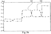
それぞれ概ね前記距離lmのところに配置されたM個の波長選択性反射手段(509−512;607−610)と、
それぞれ対応する前記波長選択性手段に関連して配置されたM個の位相調整手段(611−614;513−519;801−804)とを含み、
m(2<=m<=M)番目の前記波長選択性反射手段は、m番目の前記波長により搬送される前記光信号を反射するように構成されており、
m番目の前記位相調整手段は、m番目の前記波長選択性反射手段によって反射されたときに、選択された出力アクセス導波路に単一の自己イメージが形成されるように、m番目の前記波長によって搬送される前記光信号の前記自己イメージの位相を調整するように構成されている
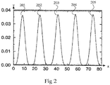
ことを特徴とするデバイス。 - m番目の前記波長によって搬送される前記光信号からのN個の前記自己イメージのそれぞれは、i番目の前記アクセス導波路から前記MMI導波路へと入射し、それぞれ位相pn,iを有し、組Piは、前記自己イメージらの位相pn,iの位相分布であり、
M個の前記位相調整手段のそれぞれは、i番目の前記入力アクセス導波路からm番目の前記波長λmによって搬送される前記光信号からの前記自己イメージの前記波長分布Piを、選択されたj番目の出力アクセス導波路の位相分布Pjに一致するように調整する
ことを特徴とする請求項1に記載のデバイス。 - M個の前記位相調整手段は、入射光の伝搬方向に対して直交する方向にN個の位相シフト器を含む
ことを特徴とする請求項1に記載のデバイス。 - m番目の前記波長選択性反射手段は、m番目の前記波長λmを反射し、それ以外の波長λk(λk≠λm)については実質的に透過となる
ことを特徴とする請求項1に記載のデバイス。 - m番目の前記波長選択性反射手段は、入射光の伝搬方向に対して実質的に直交する方向にN個の波長選択性反射手段を含む
ことを特徴とする請求項1に記載のデバイス。 - N個の前記波長選択性反射手段は、ブラッグ回折格子であることを特徴とする請求項5に記載のデバイス。
- 前記位相調整手段の少なくとも一つは、i番目の前記入力アクセス導波路からの自己イメージについての前記位相分布Piが、選択された出力アクセス導波路の位相分布Pjに一致するように、光の伝搬方向において、N個の前記波長選択性反射手段のそれぞれを中央線からずらすことによって実現することを特徴とする請求項6に記載のデバイス。
- 前記自己イメージの位相を調整するための前記位相シフト器は、MxN個の前記波長選択性反射手段の光の伝搬方向に対してそれぞれ前方に配置されていることを特徴とする請求項3に記載のデバイス。
- 前記自己イメージの位相を調整するための前記位相シフト器は、MxN個の前記波長選択性反射手段の光の伝搬方向に対してそれぞれ前方に配置される第1の部分と、MxN個の前記波長選択性反射手段の後方に配置される第2の部分とを含むことを特徴とする請求項3に記載のデバイス。
- それぞれ異なる波長λmによって搬送されるM(Mは2以上の整数)個の光信号をスイッチングするデバイスであって、
前記デバイスは、第1の側にアクセス導波路への接続経路となるN(Nは2以上の整数)個のアクセス端子を有する多モード干渉(MMI)導波路(606)を含み、
前記MMI導波路は、i(i<=N)番目のアクセス導波路において該MMI導波路へと伝搬される前記各光信号が、前記アクセス端子から距離lmとなる該MMI導波路内部のところにN個の自己イメージを生成することができるような寸法であり、
それぞれ概ね前記距離lmのところに配置されたM個の波長選択性反射手段(607−610)と、
それぞれ対応する前記波長選択性手段に関連して配置されたM個の位相調整手段(611−614)とを含み、
m(2<=m<=M)番目の前記波長選択性反射手段は、m番目の前記波長により搬送される前記光信号を反射するように構成されており、
m番目の前記位相調整手段は、m番目の前記波長選択性反射手段によって反射されたときに、選択された出力アクセス導波路に単一の自己イメージが形成されるように、m番目の前記波長によって搬送される前記光信号の前記自己イメージの位相を調整するように構成されており、
前記波長らによって搬送される前記光信号らのそれぞれの出力アクセス導波路を動的に選択するために、前記位相調整手段のそれぞれを制御するスイッチ制御手段(615)とを含む
ことを特徴とするデバイス。 - 前記位相調整手段のそれぞれは、電流、電圧または熱の応用によって制御可能かつ調整可能な反射係数を有する光透過部を含み、
前記スイッチ制御部は、前記位相調整手段のそれぞれに適用される電流、電圧または熱を制御することによって自己イメージについての位相分布を制御するように構成されている
ことを特徴とする請求項10に記載のデバイス。 - それぞれ異なる波長λmによって搬送されるM(Mは2以上の整数)個の光信号を合波、分波またはスイッチングする方法であって、
第1の側にアクセス導波路への接続経路となるN(Nは2以上の整数)個のアクセス端子を有する多モード干渉(MMI)導波路(106)を利用するものであり、前記MMI導波路は、i(i<=N)番目のアクセス導波路において該MMI導波路へと伝搬される前記各光信号が、前記アクセス端子から距離lmとなる該MMI導波路内部のところにN個の自己イメージを生成することができるような寸法であり、
前記方法は、
選択された出力アクセス導波路に単一の自己イメージが形成されるように、m番目の前記波長によって搬送される前記光信号の前記自己イメージの位相を調整するステップと、
m(2<=m<=M)番目の前記波長により搬送される前記光信号についてN個の前記自己イメージが出現する前記MMI導波路内の位置において、m番目の該波長により搬送される該光信号を反射するステップと
を含むことを特徴とする方法。 - m番目の前記波長によって搬送される前記光信号からのN個の前記自己イメージのそれぞれは、i番目の前記アクセス導波路から前記MMI導波路へと入射し、それぞれ位相pn,iを有し、組Piは、前記自己イメージらの位相pn,iの位相分布であり、
i番目の前記入力アクセス導波路からm番目の前記波長λmによって搬送される光信号からの自己イメージの前記波長分布Piを、選択されたj番目の出力アクセス導波路の位相分布Pjに一致するように調整する
ことを特徴とする請求項12に記載の方法。 - i番目の前記入力アクセス導波路からm番目の前記波長λmによって搬送される前記光信号からの前記自己イメージの前記波長分布Piを、動的に選択されたj番目の出力アクセス導波路の位相分布Pjと一致するよう動的に前記位相の調整を制御するステップをさらに含むことを特徴とする請求項12に記載の方法。
Applications Claiming Priority (2)
| Application Number | Priority Date | Filing Date | Title |
|---|---|---|---|
| SE0103725A SE521419C2 (sv) | 2001-11-09 | 2001-11-09 | MMI-baserad anordning |
| PCT/SE2002/002018 WO2003041319A2 (en) | 2001-11-09 | 2002-11-06 | Mmi based device |
Publications (2)
| Publication Number | Publication Date |
|---|---|
| JP2005509191A true JP2005509191A (ja) | 2005-04-07 |
| JP4611631B2 JP4611631B2 (ja) | 2011-01-12 |
Family
ID=20285917
Family Applications (1)
| Application Number | Title | Priority Date | Filing Date |
|---|---|---|---|
| JP2003543234A Expired - Fee Related JP4611631B2 (ja) | 2001-11-09 | 2002-11-06 | Mmiベースの装置 |
Country Status (9)
| Country | Link |
|---|---|
| US (1) | US7349628B2 (ja) |
| EP (1) | EP1451959B1 (ja) |
| JP (1) | JP4611631B2 (ja) |
| CN (1) | CN1582547A (ja) |
| AT (1) | ATE416524T1 (ja) |
| DE (1) | DE60230180D1 (ja) |
| SE (1) | SE521419C2 (ja) |
| TW (1) | TWI223936B (ja) |
| WO (1) | WO2003041319A2 (ja) |
Families Citing this family (6)
| Publication number | Priority date | Publication date | Assignee | Title |
|---|---|---|---|---|
| DE102008044818A1 (de) * | 2008-08-28 | 2010-03-04 | Fraunhofer-Gesellschaft zur Förderung der angewandten Forschung e.V. | Multimode-Interferenzkoppler und Verfahren zu seiner konstruktiven Ausgestaltung |
| US9116298B2 (en) | 2013-03-15 | 2015-08-25 | Mitsubishi Electric Research Laboratories, Inc. | Multi-mode interference device |
| US9097852B2 (en) | 2013-03-15 | 2015-08-04 | Mitsubishi Electric Research Laboratories, Inc. | Multi-mode interference device |
| US20150086158A1 (en) * | 2013-09-26 | 2015-03-26 | Mitsubishi Electric Corporation | Multi-Mode Phase-Shifting Interference Device |
| WO2023061376A1 (en) * | 2021-10-12 | 2023-04-20 | Fizetta Limited | Optical multimode wavelength division multiplexing and demultiplexing devices and transmission systems implementing the same |
| US11609392B1 (en) * | 2022-02-24 | 2023-03-21 | X Development Llc | Photonic coupler |
Citations (7)
| Publication number | Priority date | Publication date | Assignee | Title |
|---|---|---|---|---|
| JPH06503898A (ja) * | 1990-12-20 | 1994-04-28 | イギリス国 | 信号ルーチングデバイス |
| JPH08512429A (ja) * | 1993-07-03 | 1996-12-24 | イギリス国 | レーザ装置 |
| WO2000018042A2 (en) * | 1998-09-22 | 2000-03-30 | Telefonaktiebolaget Lm Ericsson (Publ) | Tuneable add/drop multiplexer |
| WO2001033758A1 (en) * | 1999-11-05 | 2001-05-10 | Telefonaktiebolaget Lm Ericsson | A device and a method for optical multiplexing/demultiplexing |
| JP2001166160A (ja) * | 1999-12-03 | 2001-06-22 | Fujitsu Ltd | 光導波路、光源、および光多重化器 |
| JP2001514766A (ja) * | 1997-03-07 | 2001-09-11 | テレフオンアクチーボラゲツト エル エム エリクソン(パブル) | 少なくとも1つのブラッグ格子構造体を含む波長選択光デバイス |
| WO2001073994A1 (en) * | 2000-03-24 | 2001-10-04 | Telefonaktiebolaget L M Ericsson | Device and method for optical add/drop multiplexing |
Family Cites Families (9)
| Publication number | Priority date | Publication date | Assignee | Title |
|---|---|---|---|---|
| GB2317023B (en) * | 1997-02-07 | 1998-07-29 | Bookham Technology Ltd | A tapered rib waveguide |
| SE508871C2 (sv) * | 1997-03-07 | 1998-11-09 | Ericsson Telefon Ab L M | Förfarande och anordning för omkoppling av optiska våglängdsmultiplexerade kanaler |
| US5862288A (en) * | 1997-04-21 | 1999-01-19 | The United States Of America As Represented By The Secretary Of The Army | Self-imaging waveguide devices for wavelength division multiplexing applications |
| US5889906A (en) * | 1997-05-28 | 1999-03-30 | Lucent Technologies Inc. | Signal router with coupling of multiple waveguide modes for provicing a shaped multi-channel radiation pattern |
| US5953467A (en) * | 1997-09-23 | 1999-09-14 | Lucent Technologies Inc. | Switchable optical filter |
| KR100293954B1 (ko) * | 1999-05-11 | 2001-06-15 | 윤종용 | 평탄한 주파수 응답을 가진 저손실 광파장 분할기 |
| US6603893B1 (en) * | 2001-03-27 | 2003-08-05 | Intel Corporation | Method and apparatus for switching an optical beam in a semiconductor substrate |
| US6674929B2 (en) * | 2001-06-01 | 2004-01-06 | Lightcross, Inc. | Tunable optical filter |
| US6892021B2 (en) * | 2001-09-17 | 2005-05-10 | Lucent Technologies Inc. | Dynamic gain equalization arrangement for optical signals |
-
2001
- 2001-11-09 SE SE0103725A patent/SE521419C2/sv not_active IP Right Cessation
- 2001-12-24 TW TW090132030A patent/TWI223936B/zh not_active IP Right Cessation
-
2002
- 2002-11-06 JP JP2003543234A patent/JP4611631B2/ja not_active Expired - Fee Related
- 2002-11-06 CN CNA028221494A patent/CN1582547A/zh active Pending
- 2002-11-06 US US10/493,978 patent/US7349628B2/en not_active Expired - Fee Related
- 2002-11-06 WO PCT/SE2002/002018 patent/WO2003041319A2/en not_active Ceased
- 2002-11-06 EP EP02783921A patent/EP1451959B1/en not_active Expired - Lifetime
- 2002-11-06 AT AT02783921T patent/ATE416524T1/de not_active IP Right Cessation
- 2002-11-06 DE DE60230180T patent/DE60230180D1/de not_active Expired - Lifetime
Patent Citations (7)
| Publication number | Priority date | Publication date | Assignee | Title |
|---|---|---|---|---|
| JPH06503898A (ja) * | 1990-12-20 | 1994-04-28 | イギリス国 | 信号ルーチングデバイス |
| JPH08512429A (ja) * | 1993-07-03 | 1996-12-24 | イギリス国 | レーザ装置 |
| JP2001514766A (ja) * | 1997-03-07 | 2001-09-11 | テレフオンアクチーボラゲツト エル エム エリクソン(パブル) | 少なくとも1つのブラッグ格子構造体を含む波長選択光デバイス |
| WO2000018042A2 (en) * | 1998-09-22 | 2000-03-30 | Telefonaktiebolaget Lm Ericsson (Publ) | Tuneable add/drop multiplexer |
| WO2001033758A1 (en) * | 1999-11-05 | 2001-05-10 | Telefonaktiebolaget Lm Ericsson | A device and a method for optical multiplexing/demultiplexing |
| JP2001166160A (ja) * | 1999-12-03 | 2001-06-22 | Fujitsu Ltd | 光導波路、光源、および光多重化器 |
| WO2001073994A1 (en) * | 2000-03-24 | 2001-10-04 | Telefonaktiebolaget L M Ericsson | Device and method for optical add/drop multiplexing |
Non-Patent Citations (1)
| Title |
|---|
| JPN6008047818, H. Okayama et al., ""Multiport wavelength routers using multimode interference"", Opt. Eng., 199704, Vol.36,No.4, pp.1078−1081, US, Society of Photo−Optical Instrumentation Engineers * |
Also Published As
| Publication number | Publication date |
|---|---|
| DE60230180D1 (de) | 2009-01-15 |
| SE0103725L (sv) | 2003-05-10 |
| WO2003041319A3 (en) | 2003-09-12 |
| US7349628B2 (en) | 2008-03-25 |
| EP1451959A2 (en) | 2004-09-01 |
| ATE416524T1 (de) | 2008-12-15 |
| TWI223936B (en) | 2004-11-11 |
| CN1582547A (zh) | 2005-02-16 |
| SE521419C2 (sv) | 2003-10-28 |
| EP1451959B1 (en) | 2008-12-03 |
| JP4611631B2 (ja) | 2011-01-12 |
| SE0103725D0 (sv) | 2001-11-09 |
| US20050008365A1 (en) | 2005-01-13 |
| WO2003041319A2 (en) | 2003-05-15 |
Similar Documents
| Publication | Publication Date | Title |
|---|---|---|
| US5953467A (en) | Switchable optical filter | |
| JP3256418B2 (ja) | 光学装置 | |
| KR100922479B1 (ko) | 기판에 슬래브 도파관과 채널 도파관들을 갖는 광학 장치 | |
| US6421478B1 (en) | Tapered MMI coupler | |
| JP5117104B2 (ja) | 小型低損失アレイ導波路格子に結合された低減駆動電圧を有する非対称マッハ・ツェンダー干渉計 | |
| US6944366B2 (en) | Planar lightwave wavelength device using moveable mirrors | |
| US6597841B1 (en) | Multi-output arrayed waveguide grating demultiplexer | |
| JP4611631B2 (ja) | Mmiベースの装置 | |
| US6571031B1 (en) | Device for multiplexing/demultiplexing and method therewith | |
| US7257285B2 (en) | Wavelength-selective switch and integrated wavelength demultiplexer using stacked planar lightwave circuits | |
| US6600852B1 (en) | Wavelength selective device and switch and method thereby | |
| US6785442B2 (en) | Multi-order optical cross-connect | |
| US6754410B1 (en) | Integrated wavelength-selective cross connect | |
| JP4350044B2 (ja) | 光スイッチ装置 | |
| JP2001127705A (ja) | 光分岐多重装置 | |
| JP4748514B2 (ja) | 波長選択スイッチ | |
| JP4366955B2 (ja) | 光機能装置および光機能モジュール | |
| JP4899822B2 (ja) | 光合分波器 | |
| JP2014160217A (ja) | アレイ導波路回折格子型波長選択スイッチ | |
| JP2004246230A (ja) | 光機能装置 | |
| JP2007256367A (ja) | 光波長合分波装置 | |
| SE519912C2 (sv) | Anordning för multiplexering/demultiplexering samt förfarande därvid |
Legal Events
| Date | Code | Title | Description |
|---|---|---|---|
| A529 | Written submission of copy of amendment under article 34 pct |
Free format text: JAPANESE INTERMEDIATE CODE: A529 Effective date: 20040507 |
|
| A621 | Written request for application examination |
Free format text: JAPANESE INTERMEDIATE CODE: A621 Effective date: 20051101 |
|
| A131 | Notification of reasons for refusal |
Free format text: JAPANESE INTERMEDIATE CODE: A131 Effective date: 20080919 |
|
| A521 | Request for written amendment filed |
Free format text: JAPANESE INTERMEDIATE CODE: A523 Effective date: 20081217 |
|
| A521 | Request for written amendment filed |
Free format text: JAPANESE INTERMEDIATE CODE: A523 Effective date: 20081217 |
|
| A131 | Notification of reasons for refusal |
Free format text: JAPANESE INTERMEDIATE CODE: A131 Effective date: 20100122 |
|
| A521 | Request for written amendment filed |
Free format text: JAPANESE INTERMEDIATE CODE: A523 Effective date: 20100202 |
|
| TRDD | Decision of grant or rejection written | ||
| A01 | Written decision to grant a patent or to grant a registration (utility model) |
Free format text: JAPANESE INTERMEDIATE CODE: A01 Effective date: 20101001 |
|
| A01 | Written decision to grant a patent or to grant a registration (utility model) |
Free format text: JAPANESE INTERMEDIATE CODE: A01 |
|
| A61 | First payment of annual fees (during grant procedure) |
Free format text: JAPANESE INTERMEDIATE CODE: A61 Effective date: 20101014 |
|
| FPAY | Renewal fee payment (event date is renewal date of database) |
Free format text: PAYMENT UNTIL: 20131022 Year of fee payment: 3 |
|
| R150 | Certificate of patent or registration of utility model |
Free format text: JAPANESE INTERMEDIATE CODE: R150 |
|
| R250 | Receipt of annual fees |
Free format text: JAPANESE INTERMEDIATE CODE: R250 |
|
| R250 | Receipt of annual fees |
Free format text: JAPANESE INTERMEDIATE CODE: R250 |
|
| R250 | Receipt of annual fees |
Free format text: JAPANESE INTERMEDIATE CODE: R250 |
|
| LAPS | Cancellation because of no payment of annual fees |