JP2006032484A - 配線基板の製造方法 - Google Patents
配線基板の製造方法 Download PDFInfo
- Publication number
- JP2006032484A JP2006032484A JP2004206069A JP2004206069A JP2006032484A JP 2006032484 A JP2006032484 A JP 2006032484A JP 2004206069 A JP2004206069 A JP 2004206069A JP 2004206069 A JP2004206069 A JP 2004206069A JP 2006032484 A JP2006032484 A JP 2006032484A
- Authority
- JP
- Japan
- Prior art keywords
- wiring board
- base substrate
- manufacturing
- plating
- layer
- Prior art date
- Legal status (The legal status is an assumption and is not a legal conclusion. Google has not performed a legal analysis and makes no representation as to the accuracy of the status listed.)
- Withdrawn
Links
- 238000004519 manufacturing process Methods 0.000 title claims abstract description 38
- 238000007747 plating Methods 0.000 claims abstract description 64
- 238000000034 method Methods 0.000 claims abstract description 50
- UMGDCJDMYOKAJW-UHFFFAOYSA-N thiourea Chemical compound NC(N)=S UMGDCJDMYOKAJW-UHFFFAOYSA-N 0.000 claims abstract description 30
- 239000002904 solvent Substances 0.000 claims abstract description 19
- XSQUKJJJFZCRTK-UHFFFAOYSA-N Urea Natural products NC(N)=O XSQUKJJJFZCRTK-UHFFFAOYSA-N 0.000 claims abstract description 15
- 150000001412 amines Chemical class 0.000 claims abstract description 12
- 238000010438 heat treatment Methods 0.000 claims abstract description 8
- 239000000758 substrate Substances 0.000 claims description 51
- 238000007772 electroless plating Methods 0.000 claims description 28
- 238000004140 cleaning Methods 0.000 claims description 13
- 239000000853 adhesive Substances 0.000 claims description 12
- 230000001070 adhesive effect Effects 0.000 claims description 12
- 238000009713 electroplating Methods 0.000 abstract 3
- 239000010410 layer Substances 0.000 description 38
- 238000010586 diagram Methods 0.000 description 11
- 239000010949 copper Substances 0.000 description 5
- RYGMFSIKBFXOCR-UHFFFAOYSA-N Copper Chemical compound [Cu] RYGMFSIKBFXOCR-UHFFFAOYSA-N 0.000 description 4
- 229910052802 copper Inorganic materials 0.000 description 4
- 239000004065 semiconductor Substances 0.000 description 4
- PXHVJJICTQNCMI-UHFFFAOYSA-N Nickel Chemical compound [Ni] PXHVJJICTQNCMI-UHFFFAOYSA-N 0.000 description 3
- 230000000694 effects Effects 0.000 description 3
- 239000000463 material Substances 0.000 description 3
- HZAXFHJVJLSVMW-UHFFFAOYSA-N 2-Aminoethan-1-ol Chemical compound NCCO HZAXFHJVJLSVMW-UHFFFAOYSA-N 0.000 description 2
- ATJFFYVFTNAWJD-UHFFFAOYSA-N Tin Chemical compound [Sn] ATJFFYVFTNAWJD-UHFFFAOYSA-N 0.000 description 2
- 239000011651 chromium Substances 0.000 description 2
- 230000006866 deterioration Effects 0.000 description 2
- -1 dipropanolamine Chemical compound 0.000 description 2
- 239000010931 gold Substances 0.000 description 2
- 230000005012 migration Effects 0.000 description 2
- 238000013508 migration Methods 0.000 description 2
- 239000000203 mixture Substances 0.000 description 2
- HBVFXTAPOLSOPB-UHFFFAOYSA-N nickel vanadium Chemical compound [V].[Ni] HBVFXTAPOLSOPB-UHFFFAOYSA-N 0.000 description 2
- 239000010936 titanium Substances 0.000 description 2
- HXKKHQJGJAFBHI-UHFFFAOYSA-N 1-aminopropan-2-ol Chemical compound CC(O)CN HXKKHQJGJAFBHI-UHFFFAOYSA-N 0.000 description 1
- SBASXUCJHJRPEV-UHFFFAOYSA-N 2-(2-methoxyethoxy)ethanol Chemical compound COCCOCCO SBASXUCJHJRPEV-UHFFFAOYSA-N 0.000 description 1
- UPGSWASWQBLSKZ-UHFFFAOYSA-N 2-hexoxyethanol Chemical compound CCCCCCOCCO UPGSWASWQBLSKZ-UHFFFAOYSA-N 0.000 description 1
- QCDWFXQBSFUVSP-UHFFFAOYSA-N 2-phenoxyethanol Chemical compound OCCOC1=CC=CC=C1 QCDWFXQBSFUVSP-UHFFFAOYSA-N 0.000 description 1
- QCAHUFWKIQLBNB-UHFFFAOYSA-N 3-(3-methoxypropoxy)propan-1-ol Chemical compound COCCCOCCCO QCAHUFWKIQLBNB-UHFFFAOYSA-N 0.000 description 1
- BLFRQYKZFKYQLO-UHFFFAOYSA-N 4-aminobutan-1-ol Chemical compound NCCCCO BLFRQYKZFKYQLO-UHFFFAOYSA-N 0.000 description 1
- VYZAMTAEIAYCRO-UHFFFAOYSA-N Chromium Chemical compound [Cr] VYZAMTAEIAYCRO-UHFFFAOYSA-N 0.000 description 1
- OPKOKAMJFNKNAS-UHFFFAOYSA-N N-methylethanolamine Chemical compound CNCCO OPKOKAMJFNKNAS-UHFFFAOYSA-N 0.000 description 1
- WUGQZFFCHPXWKQ-UHFFFAOYSA-N Propanolamine Chemical compound NCCCO WUGQZFFCHPXWKQ-UHFFFAOYSA-N 0.000 description 1
- 229910020888 Sn-Cu Inorganic materials 0.000 description 1
- 229910019204 Sn—Cu Inorganic materials 0.000 description 1
- RTAQQCXQSZGOHL-UHFFFAOYSA-N Titanium Chemical compound [Ti] RTAQQCXQSZGOHL-UHFFFAOYSA-N 0.000 description 1
- 239000000956 alloy Substances 0.000 description 1
- 229910045601 alloy Inorganic materials 0.000 description 1
- XAGFODPZIPBFFR-UHFFFAOYSA-N aluminium Chemical compound [Al] XAGFODPZIPBFFR-UHFFFAOYSA-N 0.000 description 1
- 229910052782 aluminium Inorganic materials 0.000 description 1
- LHIJANUOQQMGNT-UHFFFAOYSA-N aminoethylethanolamine Chemical compound NCCNCCO LHIJANUOQQMGNT-UHFFFAOYSA-N 0.000 description 1
- 229910052804 chromium Inorganic materials 0.000 description 1
- 230000007797 corrosion Effects 0.000 description 1
- 238000005260 corrosion Methods 0.000 description 1
- 238000005520 cutting process Methods 0.000 description 1
- ZBCBWPMODOFKDW-UHFFFAOYSA-N diethanolamine Chemical compound OCCNCCO ZBCBWPMODOFKDW-UHFFFAOYSA-N 0.000 description 1
- 238000007598 dipping method Methods 0.000 description 1
- 229920006332 epoxy adhesive Polymers 0.000 description 1
- 150000002169 ethanolamines Chemical class 0.000 description 1
- LYCAIKOWRPUZTN-UHFFFAOYSA-N ethylene glycol Natural products OCCO LYCAIKOWRPUZTN-UHFFFAOYSA-N 0.000 description 1
- 239000011888 foil Substances 0.000 description 1
- PCHJSUWPFVWCPO-UHFFFAOYSA-N gold Chemical compound [Au] PCHJSUWPFVWCPO-UHFFFAOYSA-N 0.000 description 1
- 229910052737 gold Inorganic materials 0.000 description 1
- WGCNASOHLSPBMP-UHFFFAOYSA-N hydroxyacetaldehyde Natural products OCC=O WGCNASOHLSPBMP-UHFFFAOYSA-N 0.000 description 1
- 238000007689 inspection Methods 0.000 description 1
- 229940102253 isopropanolamine Drugs 0.000 description 1
- 239000004973 liquid crystal related substance Substances 0.000 description 1
- 238000004020 luminiscence type Methods 0.000 description 1
- 229910052759 nickel Inorganic materials 0.000 description 1
- 238000000059 patterning Methods 0.000 description 1
- 239000002798 polar solvent Substances 0.000 description 1
- 239000002356 single layer Substances 0.000 description 1
- 238000003756 stirring Methods 0.000 description 1
- 239000004094 surface-active agent Substances 0.000 description 1
- 230000008646 thermal stress Effects 0.000 description 1
- 150000003585 thioureas Chemical class 0.000 description 1
- 229910001432 tin ion Inorganic materials 0.000 description 1
- 229910052719 titanium Inorganic materials 0.000 description 1
- MAKDTFFYCIMFQP-UHFFFAOYSA-N titanium tungsten Chemical compound [Ti].[W] MAKDTFFYCIMFQP-UHFFFAOYSA-N 0.000 description 1
- 230000009466 transformation Effects 0.000 description 1
- JLGLQAWTXXGVEM-UHFFFAOYSA-N triethylene glycol monomethyl ether Chemical compound COCCOCCOCCO JLGLQAWTXXGVEM-UHFFFAOYSA-N 0.000 description 1
- WFKWXMTUELFFGS-UHFFFAOYSA-N tungsten Chemical compound [W] WFKWXMTUELFFGS-UHFFFAOYSA-N 0.000 description 1
- 229910052721 tungsten Inorganic materials 0.000 description 1
- 239000010937 tungsten Substances 0.000 description 1
Images


Landscapes
- Chemically Coating (AREA)
- Manufacturing Of Printed Wiring (AREA)
- Wire Bonding (AREA)
Abstract
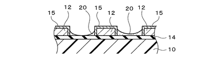
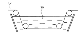
【解決手段】 チオ尿素及びその誘導体の少なくとも一方を含有するめっき液20を利用して、ベース基板10に設けられた配線パターン12に第1の無電解めっき処理を行って、厚みが0.1μm未満のめっき層15を形成する。アミンを含有する溶剤30を利用してベース基板10を洗浄する。ベース基板10に、めっき層15を部分的に覆うレジスト層40を形成する。めっき層15におけるレジスト層40からの露出部に、第2の無電解めっき処理を行う。第1の無電解めっき処理工程とレジスト層40を形成する工程との間では、加熱工程を行わない。
【選択図】 図8
Description
前記ベース基板に、前記めっき層を部分的に覆うレジスト層を形成すること、及び、
前記めっき層における前記レジスト層からの露出部に、第2の無電解めっき処理を行うことを含み、
前記第1の無電解めっき処理工程と前記レジスト層を形成する工程との間では、加熱工程を行わない。本発明によれば、第1の無電解めっき処理によって、厚みが0.1μm未満のめっき層を形成する。そのため、ベース基板(あるいはめっき層)を加熱する工程を行わなかった場合でも、レジスト層を形成するまでにウイスカーが発生することを防止することができる。そのため、効率よく配線基板を製造することができる。
(2)この配線基板の製造方法において、
前記第1の無電解めっき処理工程を、チオ尿素及びその誘導体の少なくとも一方を含有するめっき液を利用して行い、
前記第1の無電解めっき処理工程と前記レジスト層を形成する工程との間に、アミンを含有する溶剤を利用して前記ベース基板を洗浄することをさらに含んでもよい。
(3)この配線基板の製造方法において、
前記第2の無電解めっき処理工程を、チオ尿素及びその誘導体の少なくとも一方を含有するめっき液を利用して行い、
前記第2の無電解めっき処理工程後に、アミンを含有する溶剤を利用して前記ベース基板を洗浄することをさらに含んでもよい。
(4)この配線基板の製造方法において、
前記配線パターンは、接着剤を介して前記ベース基板に固着されていてもよい。
Claims (4)
- ベース基板に設けられた配線パターンに第1の無電解めっき処理を行って、厚みが0.1μm未満のめっき層を形成すること、
前記ベース基板に、前記めっき層を部分的に覆うレジスト層を形成すること、及び、
前記めっき層における前記レジスト層からの露出部に、第2の無電解めっき処理を行うことを含み、
前記第1の無電解めっき処理工程と前記レジスト層を形成する工程との間では、加熱工程を行わない配線基板の製造方法。 - 請求項1記載の配線基板の製造方法において、
前記第1の無電解めっき処理工程を、チオ尿素及びその誘導体の少なくとも一方を含有するめっき液を利用して行い、
前記第1の無電解めっき処理工程と前記レジスト層を形成する工程との間に、アミンを含有する溶剤を利用して前記ベース基板を洗浄することをさらに含む配線基板の製造方法。 - 請求項1又は請求項2記載の配線基板の製造方法において、
前記第2の無電解めっき処理工程を、チオ尿素及びその誘導体の少なくとも一方を含有するめっき液を利用して行い、
前記第2の無電解めっき処理工程後に、アミンを含有する溶剤を利用して前記ベース基板を洗浄することをさらに含む配線基板の製造方法。 - 請求項1から請求項3のいずれかに記載の配線基板の製造方法において、
前記配線パターンは、接着剤を介して前記ベース基板に固着されてなる配線基板の製造方法。
Priority Applications (1)
| Application Number | Priority Date | Filing Date | Title |
|---|---|---|---|
| JP2004206069A JP2006032484A (ja) | 2004-07-13 | 2004-07-13 | 配線基板の製造方法 |
Applications Claiming Priority (1)
| Application Number | Priority Date | Filing Date | Title |
|---|---|---|---|
| JP2004206069A JP2006032484A (ja) | 2004-07-13 | 2004-07-13 | 配線基板の製造方法 |
Publications (1)
| Publication Number | Publication Date |
|---|---|
| JP2006032484A true JP2006032484A (ja) | 2006-02-02 |
Family
ID=35898495
Family Applications (1)
| Application Number | Title | Priority Date | Filing Date |
|---|---|---|---|
| JP2004206069A Withdrawn JP2006032484A (ja) | 2004-07-13 | 2004-07-13 | 配線基板の製造方法 |
Country Status (1)
| Country | Link |
|---|---|
| JP (1) | JP2006032484A (ja) |
Citations (6)
| Publication number | Priority date | Publication date | Assignee | Title |
|---|---|---|---|---|
| JPH043491A (ja) * | 1990-04-20 | 1992-01-08 | Nikko Kyodo Co Ltd | 回路又はリードフレームのめっき方法 |
| JPH0621621A (ja) * | 1992-05-08 | 1994-01-28 | C Uyemura & Co Ltd | 回路パターンの形成方法 |
| JPH09130050A (ja) * | 1994-12-01 | 1997-05-16 | Ibiden Co Ltd | 多層プリント配線板およびその製造方法 |
| JP2003289060A (ja) * | 2002-01-28 | 2003-10-10 | Mitsubishi Chemicals Corp | 半導体デバイス用基板の洗浄液および洗浄方法 |
| JP2004084056A (ja) * | 2002-07-05 | 2004-03-18 | Ebara Corp | 無電解めっき装置および無電解めっき後の洗浄方法 |
| WO2004024985A1 (ja) * | 2002-09-11 | 2004-03-25 | Inspire Technology Resource Management Corporation | 無電解メッキ液、及びこれを用いた無電解メッキ方法及び無電解メッキ被処理物 |
-
2004
- 2004-07-13 JP JP2004206069A patent/JP2006032484A/ja not_active Withdrawn
Patent Citations (6)
| Publication number | Priority date | Publication date | Assignee | Title |
|---|---|---|---|---|
| JPH043491A (ja) * | 1990-04-20 | 1992-01-08 | Nikko Kyodo Co Ltd | 回路又はリードフレームのめっき方法 |
| JPH0621621A (ja) * | 1992-05-08 | 1994-01-28 | C Uyemura & Co Ltd | 回路パターンの形成方法 |
| JPH09130050A (ja) * | 1994-12-01 | 1997-05-16 | Ibiden Co Ltd | 多層プリント配線板およびその製造方法 |
| JP2003289060A (ja) * | 2002-01-28 | 2003-10-10 | Mitsubishi Chemicals Corp | 半導体デバイス用基板の洗浄液および洗浄方法 |
| JP2004084056A (ja) * | 2002-07-05 | 2004-03-18 | Ebara Corp | 無電解めっき装置および無電解めっき後の洗浄方法 |
| WO2004024985A1 (ja) * | 2002-09-11 | 2004-03-25 | Inspire Technology Resource Management Corporation | 無電解メッキ液、及びこれを用いた無電解メッキ方法及び無電解メッキ被処理物 |
Similar Documents
| Publication | Publication Date | Title |
|---|---|---|
| JP5850954B2 (ja) | 非導電性基板の表面上に連続導電性回路を作製するための無害技法 | |
| JP6092489B1 (ja) | 無電解めっきのための前処理方法 | |
| JPH0748584B2 (ja) | プリント回路及びその作成法 | |
| CN101994104A (zh) | 非电解镍-钯-金镀敷方法、镀敷处理物、印刷布线板、内插板以及半导体装置 | |
| KR20100007920A (ko) | 접속 단자, 접속 단자를 이용한 반도체 패키지 및 반도체 패키지의 제조 방법 | |
| JP4332736B2 (ja) | 配線基板の製造方法 | |
| US20160262271A1 (en) | Method for manufacturing a double-sided printed circuit board | |
| WO2013082054A1 (en) | Fabricating a conductive trace structure and substrate having the structure | |
| KR101917018B1 (ko) | 적층체의 에칭 방법과 그것을 이용한 프린트 배선 기판의 제조 방법 | |
| JP2016219559A5 (ja) | ||
| KR20110038457A (ko) | 무전해 니켈 도금층을 갖는 금속배선 구조 및 그 제조방법 | |
| CN102505132B (zh) | 封装基板表面电镀方法 | |
| US9049779B2 (en) | Electrical components and methods of manufacturing electrical components | |
| JP3807505B2 (ja) | 配線基板の製造方法 | |
| JP2006032484A (ja) | 配線基板の製造方法 | |
| JP2006032483A (ja) | 配線基板の製造方法 | |
| JP2009520351A (ja) | 銀めっきに超音波を使用する方法 | |
| CN103813657A (zh) | 形成有局部镀铜的柔性印刷基板的厚度最小化方法 | |
| KR101994720B1 (ko) | 반도체 내장기판 및 그 제조 방법 | |
| JP2000236161A (ja) | プリント配線板の製造方法 | |
| JP2025039059A (ja) | 金属-セラミックス回路基板の製造方法 | |
| JPH1117331A (ja) | 可撓性回路基板の製造法 | |
| JP5562550B2 (ja) | はんだ被着方法 | |
| JP2007173414A (ja) | テープ基板及びその製造方法 | |
| JPH032378A (ja) | 透明導電膜の欠落部の修復方法 |
Legal Events
| Date | Code | Title | Description |
|---|---|---|---|
| RD04 | Notification of resignation of power of attorney |
Free format text: JAPANESE INTERMEDIATE CODE: A7424 Effective date: 20060112 |
|
| A621 | Written request for application examination |
Free format text: JAPANESE INTERMEDIATE CODE: A621 Effective date: 20070425 |
|
| A977 | Report on retrieval |
Free format text: JAPANESE INTERMEDIATE CODE: A971007 Effective date: 20090925 |
|
| A131 | Notification of reasons for refusal |
Free format text: JAPANESE INTERMEDIATE CODE: A131 Effective date: 20091007 |
|
| A761 | Written withdrawal of application |
Free format text: JAPANESE INTERMEDIATE CODE: A761 Effective date: 20091204 |