JP2006157263A - 固体撮像装置 - Google Patents
固体撮像装置 Download PDFInfo
- Publication number
- JP2006157263A JP2006157263A JP2004342432A JP2004342432A JP2006157263A JP 2006157263 A JP2006157263 A JP 2006157263A JP 2004342432 A JP2004342432 A JP 2004342432A JP 2004342432 A JP2004342432 A JP 2004342432A JP 2006157263 A JP2006157263 A JP 2006157263A
- Authority
- JP
- Japan
- Prior art keywords
- signal
- vertical
- unit
- signals
- effective pixel
- Prior art date
- Legal status (The legal status is an assumption and is not a legal conclusion. Google has not performed a legal analysis and makes no representation as to the accuracy of the status listed.)
- Granted
Links
Images


Classifications
-
- H—ELECTRICITY
- H04—ELECTRIC COMMUNICATION TECHNIQUE
- H04N—PICTORIAL COMMUNICATION, e.g. TELEVISION
- H04N25/00—Circuitry of solid-state image sensors [SSIS]; Control thereof
- H04N25/60—Noise processing, e.g. detecting, correcting, reducing or removing noise
- H04N25/67—Noise processing, e.g. detecting, correcting, reducing or removing noise applied to fixed-pattern noise, e.g. non-uniformity of response
- H04N25/671—Noise processing, e.g. detecting, correcting, reducing or removing noise applied to fixed-pattern noise, e.g. non-uniformity of response for non-uniformity detection or correction
- H04N25/677—Noise processing, e.g. detecting, correcting, reducing or removing noise applied to fixed-pattern noise, e.g. non-uniformity of response for non-uniformity detection or correction for reducing the column or line fixed pattern noise
-
- H—ELECTRICITY
- H04—ELECTRIC COMMUNICATION TECHNIQUE
- H04N—PICTORIAL COMMUNICATION, e.g. TELEVISION
- H04N25/00—Circuitry of solid-state image sensors [SSIS]; Control thereof
- H04N25/60—Noise processing, e.g. detecting, correcting, reducing or removing noise
- H04N25/618—Noise processing, e.g. detecting, correcting, reducing or removing noise for random or high-frequency noise
-
- H—ELECTRICITY
- H04—ELECTRIC COMMUNICATION TECHNIQUE
- H04N—PICTORIAL COMMUNICATION, e.g. TELEVISION
- H04N25/00—Circuitry of solid-state image sensors [SSIS]; Control thereof
- H04N25/60—Noise processing, e.g. detecting, correcting, reducing or removing noise
- H04N25/62—Detection or reduction of noise due to excess charges produced by the exposure, e.g. smear, blooming, ghost image, crosstalk or leakage between pixels
- H04N25/628—Detection or reduction of noise due to excess charges produced by the exposure, e.g. smear, blooming, ghost image, crosstalk or leakage between pixels for reducing horizontal stripes caused by saturated regions of CMOS sensors
-
- H—ELECTRICITY
- H04—ELECTRIC COMMUNICATION TECHNIQUE
- H04N—PICTORIAL COMMUNICATION, e.g. TELEVISION
- H04N25/00—Circuitry of solid-state image sensors [SSIS]; Control thereof
- H04N25/60—Noise processing, e.g. detecting, correcting, reducing or removing noise
- H04N25/63—Noise processing, e.g. detecting, correcting, reducing or removing noise applied to dark current
- H04N25/633—Noise processing, e.g. detecting, correcting, reducing or removing noise applied to dark current by using optical black pixels
-
- H—ELECTRICITY
- H04—ELECTRIC COMMUNICATION TECHNIQUE
- H04N—PICTORIAL COMMUNICATION, e.g. TELEVISION
- H04N25/00—Circuitry of solid-state image sensors [SSIS]; Control thereof
- H04N25/70—SSIS architectures; Circuits associated therewith
- H04N25/76—Addressed sensors, e.g. MOS or CMOS sensors
- H04N25/77—Pixel circuitry, e.g. memories, A/D converters, pixel amplifiers, shared circuits or shared components
- H04N25/772—Pixel circuitry, e.g. memories, A/D converters, pixel amplifiers, shared circuits or shared components comprising A/D, V/T, V/F, I/T or I/F converters
-
- H—ELECTRICITY
- H04—ELECTRIC COMMUNICATION TECHNIQUE
- H04N—PICTORIAL COMMUNICATION, e.g. TELEVISION
- H04N25/00—Circuitry of solid-state image sensors [SSIS]; Control thereof
- H04N25/70—SSIS architectures; Circuits associated therewith
- H04N25/76—Addressed sensors, e.g. MOS or CMOS sensors
- H04N25/78—Readout circuits for addressed sensors, e.g. output amplifiers or A/D converters
Landscapes
- Engineering & Computer Science (AREA)
- Multimedia (AREA)
- Signal Processing (AREA)
- Transforming Light Signals Into Electric Signals (AREA)
- Solid State Image Pick-Up Elements (AREA)
Abstract
【解決手段】有効画素部およびオプティカルブラック部が存在する撮像部11から複数の垂直信号線に読み出された画素信号をAD変換するAD変換回路13と、AD変換により得られた画素信号が順次入力し、演算処理を行う信号処理回路部21を有する。信号処理回路部は、撮像領域の垂直方向端部のOB部から読出された複数ラインの出力信号が第1の所定レベルより大きいか第2の所定レベルより小さい場合は、各所定レベルでスライスし、複数ラインの信号を加算平均化し、有効画素信号に対して加減算する縦筋補正回路部と、水平ラインの読出しスタート側のOB部の出力信号を信号レベルの大小順位に並べ替え、並べ替えた中心近傍の複数の画素の信号の平均値を有効画素信号に対して加減算する横筋補正回路部を備える。
【選択図】 図1
Description
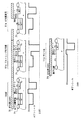
図1は、本発明の第1の実施形態に係る縦筋・横筋補正回路を含むデジタル信号処理回路部を混載したCMOSイメージセンサの全体構成の一例を示す。
図9は、本発明の第1の実施形態の変形例に係るCMOSイメージセンサの変形例の全体構成の一例を示すブロック図である。
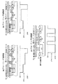
図11(a)は、本発明の第2の実施形態の変形例に係るCMOSイメージセンサにおけるセンサコア部10のレイアウトの一例および信号処理回路部21aのブロック構成の一例を示す。
Claims (5)
- 光電変換素子と光電変換した信号電荷を電圧に変換する検出部が二次元的に配置された撮像領域に存在し、前記光電変換素子に光が入射する領域である有効画素部および前記光電変換素子が遮光された領域であるオプティカルブラック部と、
前記撮像領域から複数の垂直信号線に読み出された画素信号をそれぞれデジタル信号に変換する複数のカラム型のAD変換回路と、
前記複数のカラム型のAD変換回路により得られたデジタル画素信号が順次入力し、所定の演算処理を行って映像信号を得る信号処理回路部
とを具備する固体撮像装置であって、
前記信号処理回路部は、前記撮像領域の垂直方向の端部に配置されている前記オプティカルブラック部から読出された複数ラインの出力信号が第1の所定レベルより大きいか第2の所定レベルより小さい場合は、複数ラインの出力信号を各所定レベルでスライスし、複数ラインの信号を垂直方向に加算平均化し、前記有効画素部の有効画素の出力信号に対して加減算する縦筋補正回路部を備えたことを特徴とする固体撮像装置。 - 光電変換素子と光電変換した信号電荷を電圧に変換する検出部が二次元的に配置された撮像領域に存在し、前記光電変換素子に光が入射する領域である有効画素部および前記光電変換素子が遮光された領域であるオプティカルブラック部と、
前記撮像領域から複数の垂直信号線に読み出された画素信号をそれぞれデジタル信号に変換する複数のカラム型のAD変換回路と、
前記複数のカラム型のAD変換回路により得られたデジタル画素信号が順次入力し、所定の演算処理を行って映像信号を得る信号処理回路部
とを具備する固体撮像装置であって、
前記信号処理回路部は、前記オプティカルブラック部のうちで水平ラインの読出しスタート側に配置された部分の出力信号を1水平ライン毎に信号レベルの大信号画素を除去し、残りの複数の画素の信号の平均値を前記同一水平ラインの有効画素部の有効画素の信号に対して加減算する横筋補正回路を備えたことを特徴とする固体撮像装置。 - 前記信号処理回路部は、前記撮像領域の垂直方向の端部に配置されている前記光電変換素子が形成されていない画素領域である空打ち部から読出された複数ラインの出力信号が第1の所定レベルより大きいか第2の所定レベルより小さい場合は、複数ラインの出力信号を各所定レベルでスライスし、複数ラインの信号を垂直方向に加算平均化し、前記有効画素部の有効画素の出力信号に対して加減算する縦筋補正回路部
をさらに備えたことを特徴とする請求項2記載の固体撮像装置。 - 前記撮像領域の垂直信号線に接続されている負荷トランジスタのゲートに与えるバイアス電圧を発生する第1のバイアス回路と、
前記負荷トランジスタのゲート線に前記第1のバイアス電圧または接地電位を選択的に接続する第1のスイッチ用トランジスタと、
前記撮像領域のAD変換回路で発生する縦筋ノイズを補正するために用いられるバイアス電圧を発生する第2のバイアス回路と、
前記撮像領域の垂直信号線の一端側と前記バイアス回路の出力ノードとの間に挿入され、前記第2のバイアス回路で発生されたバイアス電圧を前記垂直信号線に選択的に接続するスイッチ用トランジスタ
とをさらに具備することを特徴とする請求項1記載の固体撮像装置。 - 前記撮像領域の垂直方向の端部には、前記光電変換素子が形成されていない画素領域である空打ち部が存在し、前記オプティカルブラック部は、前記空打ち部と前記有効画素部との間に存在するブルーミング対策部を含み、前記ブルーミング対策部は、前記検出部が電源に接続されていることを特徴とする請求項1記載の固体撮像装置。
Priority Applications (5)
| Application Number | Priority Date | Filing Date | Title |
|---|---|---|---|
| JP2004342432A JP4625685B2 (ja) | 2004-11-26 | 2004-11-26 | 固体撮像装置 |
| US11/283,824 US7868935B2 (en) | 2004-11-26 | 2005-11-22 | Solid-state imaging apparatus |
| EP05025761A EP1662774A3 (en) | 2004-11-26 | 2005-11-25 | Solid-state imaging apparatus |
| CNB2005101285396A CN100438585C (zh) | 2004-11-26 | 2005-11-28 | 固体摄像器件 |
| US12/830,120 US8228402B2 (en) | 2004-11-26 | 2010-07-02 | Solid-state imaging apparatus with two light proof optical black sections |
Applications Claiming Priority (1)
| Application Number | Priority Date | Filing Date | Title |
|---|---|---|---|
| JP2004342432A JP4625685B2 (ja) | 2004-11-26 | 2004-11-26 | 固体撮像装置 |
Publications (2)
| Publication Number | Publication Date |
|---|---|
| JP2006157263A true JP2006157263A (ja) | 2006-06-15 |
| JP4625685B2 JP4625685B2 (ja) | 2011-02-02 |
Family
ID=35589539
Family Applications (1)
| Application Number | Title | Priority Date | Filing Date |
|---|---|---|---|
| JP2004342432A Expired - Fee Related JP4625685B2 (ja) | 2004-11-26 | 2004-11-26 | 固体撮像装置 |
Country Status (4)
| Country | Link |
|---|---|
| US (2) | US7868935B2 (ja) |
| EP (1) | EP1662774A3 (ja) |
| JP (1) | JP4625685B2 (ja) |
| CN (1) | CN100438585C (ja) |
Cited By (22)
| Publication number | Priority date | Publication date | Assignee | Title |
|---|---|---|---|---|
| JP2008128892A (ja) * | 2006-11-22 | 2008-06-05 | Mitsubishi Electric Corp | 赤外線撮像装置 |
| JP2008219293A (ja) * | 2007-03-01 | 2008-09-18 | Canon Inc | 撮像装置及び撮像システム |
| JP2008301221A (ja) * | 2007-05-31 | 2008-12-11 | Fujitsu Microelectronics Ltd | 固体撮像素子および固体撮像素子を用いた信号処理方法 |
| JP2009038531A (ja) * | 2007-07-31 | 2009-02-19 | Panasonic Corp | 固体撮像装置及びその駆動方法 |
| JP2010041655A (ja) * | 2008-08-08 | 2010-02-18 | Toshiba Corp | 固体撮像装置の駆動方法 |
| JP2010520709A (ja) * | 2007-03-07 | 2010-06-10 | アルタセンズ インコーポレイテッド | 信号処理装置及び信号処理方法 |
| JP2010193042A (ja) * | 2009-02-17 | 2010-09-02 | Hoya Corp | 固定パターンノイズ除去ユニット、撮像ユニット、および電子内視鏡システム |
| WO2010116904A1 (ja) * | 2009-04-07 | 2010-10-14 | 浜松ホトニクス株式会社 | 固体撮像装置 |
| JP2011015036A (ja) * | 2009-06-30 | 2011-01-20 | Canon Inc | 撮像装置、撮像システム及びそれらの制御方法 |
| JP2011029882A (ja) * | 2009-07-24 | 2011-02-10 | Sanyo Electric Co Ltd | 電子カメラ |
| JP2011214905A (ja) * | 2010-03-31 | 2011-10-27 | Fujifilm Corp | 放射線画像検出装置 |
| US8089532B2 (en) | 2008-01-25 | 2012-01-03 | Aptina Imaging Corporation | Method and apparatus providing pixel-wise noise correction |
| JP2012109603A (ja) * | 2012-02-08 | 2012-06-07 | Lapis Semiconductor Co Ltd | 半導体装置、光測定装置、光検出装置、及び半導体装置の製造方法 |
| US8648946B2 (en) | 2011-07-04 | 2014-02-11 | Kabushiki Kaisha Toshiba | Image processing device, image processing method, and solid-state image pickup device |
| JP2014179849A (ja) * | 2013-03-15 | 2014-09-25 | Hitachi Kokusai Electric Inc | 撮像装置 |
| KR20140124408A (ko) | 2013-04-16 | 2014-10-24 | 소니 주식회사 | 고체 촬상 장치, 그 신호 처리 방법 및 전자 기기 |
| KR20150066856A (ko) * | 2013-12-09 | 2015-06-17 | 삼성전자주식회사 | 이종의 아날로그-디지털 컨버터를 포함하는 이미지 센서 |
| WO2016002382A1 (ja) * | 2014-07-04 | 2016-01-07 | シャープ株式会社 | 固体撮像素子及び電子情報機器 |
| JP2017126671A (ja) * | 2016-01-14 | 2017-07-20 | 株式会社東芝 | 固体撮像装置 |
| JP2017225871A (ja) * | 2017-10-04 | 2017-12-28 | キヤノン株式会社 | 画像処理装置、放射線撮影装置、画像処理方法、コンピュータプログラム及び記憶媒体 |
| JP2019096914A (ja) * | 2019-03-18 | 2019-06-20 | 株式会社東芝 | 固体撮像装置 |
| WO2021261229A1 (ja) * | 2020-06-23 | 2021-12-30 | ソニーセミコンダクタソリューションズ株式会社 | 光検出装置、および電子機器 |
Families Citing this family (49)
| Publication number | Priority date | Publication date | Assignee | Title |
|---|---|---|---|---|
| JP4022862B2 (ja) | 2002-06-11 | 2007-12-19 | ソニー株式会社 | 固体撮像装置及びその制御方法 |
| US7564489B1 (en) | 2005-02-18 | 2009-07-21 | Crosstek Capital, LLC | Method for reducing row noise with dark pixel data |
| JP4351658B2 (ja) * | 2005-07-21 | 2009-10-28 | マイクロン テクノロジー, インク. | メモリ容量低減化方法、メモリ容量低減化雑音低減化回路及びメモリ容量低減化装置 |
| JP4827508B2 (ja) * | 2005-12-02 | 2011-11-30 | キヤノン株式会社 | 撮像システム |
| JP2008011284A (ja) * | 2006-06-30 | 2008-01-17 | Fujitsu Ltd | 画像処理回路、撮像回路および電子機器 |
| US7545418B2 (en) * | 2006-07-17 | 2009-06-09 | Jeffery Steven Beck | Image sensor device having improved noise suppression capability and a method for supressing noise in an image sensor device |
| US8223227B2 (en) * | 2006-09-28 | 2012-07-17 | Nokia Corporation | Read out method for a CMOS imager with reduced dark current |
| US8203629B2 (en) * | 2006-10-26 | 2012-06-19 | Canon Kabushiki Kaisha | Image sensing apparatus and correction method |
| US20080117317A1 (en) * | 2006-11-17 | 2008-05-22 | Ray Alan Mentzer | Dim row suppression system and method for active pixel sensor arrays |
| JP4619375B2 (ja) * | 2007-02-21 | 2011-01-26 | ソニー株式会社 | 固体撮像装置および撮像装置 |
| JP4329833B2 (ja) * | 2007-03-20 | 2009-09-09 | ソニー株式会社 | ストリーキング補正信号生成回路、ストリーキング補正信号生成方法、プログラム、ストリーキング補正回路および撮像装置 |
| JP2009034413A (ja) * | 2007-08-03 | 2009-02-19 | Toshiba Corp | 放射線画像処理装置 |
| JP4927669B2 (ja) * | 2007-09-05 | 2012-05-09 | 浜松ホトニクス株式会社 | 固体撮像装置 |
| JP4743243B2 (ja) * | 2008-09-08 | 2011-08-10 | ソニー株式会社 | 撮像装置、黒レベルの調整方法およびプログラム |
| WO2010030574A1 (en) * | 2008-09-11 | 2010-03-18 | Zoran Corporation | Method and apparatus for post noise reduction black level correction |
| JP5311987B2 (ja) * | 2008-11-27 | 2013-10-09 | キヤノン株式会社 | 撮像装置 |
| US8970707B2 (en) * | 2008-12-17 | 2015-03-03 | Sony Computer Entertainment Inc. | Compensating for blooming of a shape in an image |
| JP5254830B2 (ja) * | 2009-02-03 | 2013-08-07 | キヤノン株式会社 | 撮像装置及びその制御方法及びプログラム |
| KR100988872B1 (ko) * | 2009-07-08 | 2010-10-20 | 주식회사 나노포토닉스 | 회전 대칭형의 광각 렌즈를 이용하여 복합 영상을 얻는 방법과 그 영상 시스템 및 하드웨어적으로 영상처리를 하는 이미지 센서 |
| JP5455798B2 (ja) * | 2009-07-16 | 2014-03-26 | キヤノン株式会社 | 画像処理装置 |
| JP2011029793A (ja) * | 2009-07-22 | 2011-02-10 | Panasonic Corp | 固体撮像装置およびカメラ |
| JP2011071730A (ja) * | 2009-09-25 | 2011-04-07 | Toshiba Corp | 黒レベル調整装置および黒レベル調整方法 |
| US20120049041A1 (en) * | 2010-09-01 | 2012-03-01 | International Business Machines Corporation | Switched rail circuitry and modified cell structure and method of manufacture and use |
| TW201216138A (en) * | 2010-10-13 | 2012-04-16 | Chunghwa Picture Tubes Ltd | Method for driving photosensor array panel |
| JP5631153B2 (ja) | 2010-10-21 | 2014-11-26 | キヤノン株式会社 | 画像処理装置、制御方法、及びプログラム |
| JP5632703B2 (ja) * | 2010-10-21 | 2014-11-26 | キヤノン株式会社 | 画像処理装置、制御方法、及びプログラム |
| JP6052622B2 (ja) * | 2011-04-22 | 2016-12-27 | パナソニックIpマネジメント株式会社 | 固体撮像装置及びその駆動方法 |
| JP2013030828A (ja) * | 2011-07-26 | 2013-02-07 | Toshiba Corp | 固体撮像装置 |
| WO2014002415A1 (ja) * | 2012-06-28 | 2014-01-03 | パナソニック株式会社 | 撮像装置 |
| KR102072359B1 (ko) * | 2013-02-27 | 2020-02-03 | 삼성전자 주식회사 | 이미지 센서 |
| JP5826968B2 (ja) * | 2013-04-25 | 2015-12-02 | オリンパス株式会社 | 撮像素子、撮像装置、内視鏡および内視鏡システム |
| CN104125420B (zh) * | 2013-04-26 | 2019-01-04 | 联咏科技股份有限公司 | 固定样式噪声移除方法 |
| TWI497997B (zh) * | 2013-05-17 | 2015-08-21 | Novatek Microelectronics Corp | 影像感測器 |
| CN104184966B (zh) * | 2013-05-28 | 2017-09-15 | 联咏科技股份有限公司 | 影像传感器 |
| KR20150014716A (ko) * | 2013-07-30 | 2015-02-09 | 삼성전자주식회사 | 이미지 센서 및 그 구동 방법 |
| JP6271926B2 (ja) | 2013-09-18 | 2018-01-31 | キヤノン株式会社 | 撮像装置、その制御方法、及びプログラム |
| US9391101B2 (en) * | 2013-11-05 | 2016-07-12 | Taiwan Semiconductor Manufacturing Company, Ltd. | Image sensor pickup region layout |
| JP6428091B2 (ja) * | 2014-09-24 | 2018-11-28 | 住友電気工業株式会社 | 赤外線イメージセンサ |
| US9560294B2 (en) | 2014-12-10 | 2017-01-31 | Semiconductor Components Industries, Llc | Systems and methods for pixel-level dark current compensation in image sensors |
| US9628730B2 (en) | 2015-01-27 | 2017-04-18 | Semiconductor Components Industries, Llc | Dark current gradient estimation using optically black pixels |
| US11297258B2 (en) * | 2015-10-01 | 2022-04-05 | Qualcomm Incorporated | High dynamic range solid state image sensor and camera system |
| JP6650779B2 (ja) * | 2016-02-19 | 2020-02-19 | キヤノン株式会社 | 撮像装置、撮像システム、撮像装置の駆動方法 |
| KR20250006310A (ko) * | 2016-02-29 | 2025-01-10 | 소니그룹주식회사 | 고체 촬상 소자 |
| JP2018101966A (ja) * | 2016-12-22 | 2018-06-28 | ソニーセミコンダクタソリューションズ株式会社 | 固体撮像素子、電子機器、および、固体撮像素子の制御方法 |
| KR102469080B1 (ko) * | 2018-02-13 | 2022-11-23 | 에스케이하이닉스 주식회사 | 비교 장치 및 그에 따른 씨모스 이미지 센서 |
| KR102493826B1 (ko) * | 2018-04-30 | 2023-01-31 | 에스케이하이닉스 주식회사 | 비교 장치 및 그에 따른 씨모스 이미지 센서 |
| EP3923563B1 (en) * | 2019-02-07 | 2024-04-03 | Mitsubishi Electric Corporation | Infrared imaging device and infrared imaging program |
| CN111353421A (zh) * | 2019-04-19 | 2020-06-30 | 神盾股份有限公司 | 光学指纹感测装置 |
| US12096148B2 (en) | 2021-11-19 | 2024-09-17 | Samsung Electronics Co., Ltd. | Image sensor device and operation method thereof |
Citations (8)
| Publication number | Priority date | Publication date | Assignee | Title |
|---|---|---|---|---|
| JPH10256522A (ja) * | 1996-07-12 | 1998-09-25 | Sony Corp | 固体撮像装置およびこれを用いたカメラ |
| JP2000224440A (ja) * | 1999-02-04 | 2000-08-11 | Matsushita Electric Ind Co Ltd | ディジタルクランプ回路 |
| JP2002077738A (ja) * | 2000-08-28 | 2002-03-15 | Nikon Corp | クランプ装置 |
| JP2002320146A (ja) * | 2001-02-19 | 2002-10-31 | Innotech Corp | 可変利得アンプ、固体撮像装置及び光信号読み出し方法 |
| JP2003023549A (ja) * | 2001-07-10 | 2003-01-24 | Matsushita Electric Ind Co Ltd | 信号直流電圧安定化回路およびそれを用いた映像機器 |
| JP2003304453A (ja) * | 2002-04-11 | 2003-10-24 | Olympus Optical Co Ltd | 撮像装置 |
| JP2004015712A (ja) * | 2002-06-11 | 2004-01-15 | Sony Corp | 固体撮像装置及びその固定パターン雑音除去方法 |
| JP2004153677A (ja) * | 2002-10-31 | 2004-05-27 | Canon Inc | 撮像装置 |
Family Cites Families (19)
| Publication number | Priority date | Publication date | Assignee | Title |
|---|---|---|---|---|
| KR100263149B1 (ko) * | 1995-09-19 | 2000-08-01 | 모리시타 요이찌 | 다크셰이딩 보정회로 |
| JPH11112885A (ja) * | 1997-10-03 | 1999-04-23 | Olympus Optical Co Ltd | カメラ |
| JP3571924B2 (ja) * | 1998-07-09 | 2004-09-29 | 株式会社東芝 | 固体撮像装置 |
| JP2000261730A (ja) | 1999-03-10 | 2000-09-22 | Matsushita Electric Ind Co Ltd | 固体撮像装置およびこれを用いたカメラ |
| JP2000287137A (ja) | 1999-03-30 | 2000-10-13 | Toshiba Corp | 固体撮像素子 |
| EP1143706A3 (en) * | 2000-03-28 | 2007-08-01 | Fujitsu Limited | Image sensor with black level control and low power consumption |
| JP2002112117A (ja) * | 2000-09-27 | 2002-04-12 | Sakai Yasue | 固体撮像装置およびシステム、相関二重サンプリング回路 |
| US6744526B2 (en) * | 2001-02-09 | 2004-06-01 | Eastman Kodak Company | Image sensor having black pixels disposed in a spaced-apart relationship from the active pixels |
| JP4489319B2 (ja) * | 2001-04-26 | 2010-06-23 | 富士通マイクロエレクトロニクス株式会社 | 固体撮像装置 |
| JP4325777B2 (ja) * | 2001-05-29 | 2009-09-02 | 株式会社リコー | 映像信号処理方法および映像信号処理装置 |
| JP3870137B2 (ja) * | 2001-08-02 | 2007-01-17 | キヤノン株式会社 | 固体撮像装置及び固体撮像システム |
| JP3879987B2 (ja) * | 2002-04-10 | 2007-02-14 | 日本ビクター株式会社 | 撮像装置 |
| JP3912672B2 (ja) * | 2002-07-05 | 2007-05-09 | ソニー株式会社 | 固体撮像装置及びその画素欠陥検査方法 |
| US7317484B2 (en) * | 2003-02-26 | 2008-01-08 | Digital Imaging Systems Gmbh | CMOS APS readout scheme that combines reset drain current and the source follower output |
| EP1614282A1 (en) * | 2003-04-17 | 2006-01-11 | Nokia Corporation | An improved mobile camera telephone |
| JP4329409B2 (ja) * | 2003-05-23 | 2009-09-09 | 株式会社ニコン | 電子カメラのシェーディング補正回路 |
| JP4333290B2 (ja) * | 2003-09-04 | 2009-09-16 | 株式会社ニコン | 黒レベル補正装置、及び電子カメラ |
| JP4161855B2 (ja) * | 2003-09-10 | 2008-10-08 | ソニー株式会社 | 固体撮像装置、駆動制御方法及び駆動制御装置 |
| US7920185B2 (en) * | 2004-06-30 | 2011-04-05 | Micron Technology, Inc. | Shielding black reference pixels in image sensors |
-
2004
- 2004-11-26 JP JP2004342432A patent/JP4625685B2/ja not_active Expired - Fee Related
-
2005
- 2005-11-22 US US11/283,824 patent/US7868935B2/en not_active Expired - Fee Related
- 2005-11-25 EP EP05025761A patent/EP1662774A3/en not_active Withdrawn
- 2005-11-28 CN CNB2005101285396A patent/CN100438585C/zh not_active Expired - Fee Related
-
2010
- 2010-07-02 US US12/830,120 patent/US8228402B2/en not_active Expired - Fee Related
Patent Citations (8)
| Publication number | Priority date | Publication date | Assignee | Title |
|---|---|---|---|---|
| JPH10256522A (ja) * | 1996-07-12 | 1998-09-25 | Sony Corp | 固体撮像装置およびこれを用いたカメラ |
| JP2000224440A (ja) * | 1999-02-04 | 2000-08-11 | Matsushita Electric Ind Co Ltd | ディジタルクランプ回路 |
| JP2002077738A (ja) * | 2000-08-28 | 2002-03-15 | Nikon Corp | クランプ装置 |
| JP2002320146A (ja) * | 2001-02-19 | 2002-10-31 | Innotech Corp | 可変利得アンプ、固体撮像装置及び光信号読み出し方法 |
| JP2003023549A (ja) * | 2001-07-10 | 2003-01-24 | Matsushita Electric Ind Co Ltd | 信号直流電圧安定化回路およびそれを用いた映像機器 |
| JP2003304453A (ja) * | 2002-04-11 | 2003-10-24 | Olympus Optical Co Ltd | 撮像装置 |
| JP2004015712A (ja) * | 2002-06-11 | 2004-01-15 | Sony Corp | 固体撮像装置及びその固定パターン雑音除去方法 |
| JP2004153677A (ja) * | 2002-10-31 | 2004-05-27 | Canon Inc | 撮像装置 |
Cited By (32)
| Publication number | Priority date | Publication date | Assignee | Title |
|---|---|---|---|---|
| JP2008128892A (ja) * | 2006-11-22 | 2008-06-05 | Mitsubishi Electric Corp | 赤外線撮像装置 |
| JP2008219293A (ja) * | 2007-03-01 | 2008-09-18 | Canon Inc | 撮像装置及び撮像システム |
| US8553114B2 (en) | 2007-03-01 | 2013-10-08 | Canon Kabushiki Kaisha | Image sensing apparatus and image sensing system |
| JP2010520709A (ja) * | 2007-03-07 | 2010-06-10 | アルタセンズ インコーポレイテッド | 信号処理装置及び信号処理方法 |
| JP2008301221A (ja) * | 2007-05-31 | 2008-12-11 | Fujitsu Microelectronics Ltd | 固体撮像素子および固体撮像素子を用いた信号処理方法 |
| US8111309B2 (en) | 2007-05-31 | 2012-02-07 | Fujitsu Semiconductor Limited | Solid-state image pickup device and signal processing method using solid-state image pickup device |
| JP2009038531A (ja) * | 2007-07-31 | 2009-02-19 | Panasonic Corp | 固体撮像装置及びその駆動方法 |
| US8089532B2 (en) | 2008-01-25 | 2012-01-03 | Aptina Imaging Corporation | Method and apparatus providing pixel-wise noise correction |
| JP2010041655A (ja) * | 2008-08-08 | 2010-02-18 | Toshiba Corp | 固体撮像装置の駆動方法 |
| JP2010193042A (ja) * | 2009-02-17 | 2010-09-02 | Hoya Corp | 固定パターンノイズ除去ユニット、撮像ユニット、および電子内視鏡システム |
| JP2010245878A (ja) * | 2009-04-07 | 2010-10-28 | Hamamatsu Photonics Kk | 固体撮像装置 |
| WO2010116904A1 (ja) * | 2009-04-07 | 2010-10-14 | 浜松ホトニクス株式会社 | 固体撮像装置 |
| TWI497996B (zh) * | 2009-04-07 | 2015-08-21 | Hamamatsu Photonics Kk | Solid-state imaging device |
| US8854507B2 (en) | 2009-04-07 | 2014-10-07 | Hamamatsu Photonics K.K. | Solid-state imaging device |
| JP2011015036A (ja) * | 2009-06-30 | 2011-01-20 | Canon Inc | 撮像装置、撮像システム及びそれらの制御方法 |
| JP2011029882A (ja) * | 2009-07-24 | 2011-02-10 | Sanyo Electric Co Ltd | 電子カメラ |
| JP2011214905A (ja) * | 2010-03-31 | 2011-10-27 | Fujifilm Corp | 放射線画像検出装置 |
| US8648946B2 (en) | 2011-07-04 | 2014-02-11 | Kabushiki Kaisha Toshiba | Image processing device, image processing method, and solid-state image pickup device |
| JP2012109603A (ja) * | 2012-02-08 | 2012-06-07 | Lapis Semiconductor Co Ltd | 半導体装置、光測定装置、光検出装置、及び半導体装置の製造方法 |
| JP2014179849A (ja) * | 2013-03-15 | 2014-09-25 | Hitachi Kokusai Electric Inc | 撮像装置 |
| KR20140124408A (ko) | 2013-04-16 | 2014-10-24 | 소니 주식회사 | 고체 촬상 장치, 그 신호 처리 방법 및 전자 기기 |
| US9118855B2 (en) | 2013-04-16 | 2015-08-25 | Sony Corporation | Solid-state imaging device, signal processing method thereof, and electronic apparatus |
| KR20150066856A (ko) * | 2013-12-09 | 2015-06-17 | 삼성전자주식회사 | 이종의 아날로그-디지털 컨버터를 포함하는 이미지 센서 |
| KR102105409B1 (ko) * | 2013-12-09 | 2020-05-29 | 삼성전자주식회사 | 이종의 아날로그-디지털 컨버터를 포함하는 이미지 센서 |
| JPWO2016002382A1 (ja) * | 2014-07-04 | 2017-04-27 | シャープ株式会社 | 固体撮像素子及び電子情報機器 |
| US10212370B2 (en) | 2014-07-04 | 2019-02-19 | Sharp Kabushiki Kaisha | Solid-state image sensor and electronic information device |
| WO2016002382A1 (ja) * | 2014-07-04 | 2016-01-07 | シャープ株式会社 | 固体撮像素子及び電子情報機器 |
| JP2017126671A (ja) * | 2016-01-14 | 2017-07-20 | 株式会社東芝 | 固体撮像装置 |
| JP2017225871A (ja) * | 2017-10-04 | 2017-12-28 | キヤノン株式会社 | 画像処理装置、放射線撮影装置、画像処理方法、コンピュータプログラム及び記憶媒体 |
| JP2019096914A (ja) * | 2019-03-18 | 2019-06-20 | 株式会社東芝 | 固体撮像装置 |
| WO2021261229A1 (ja) * | 2020-06-23 | 2021-12-30 | ソニーセミコンダクタソリューションズ株式会社 | 光検出装置、および電子機器 |
| US12273636B2 (en) | 2020-06-23 | 2025-04-08 | Sony Semiconductor Solutions Corporation | Photodetection device and electronic apparatus |
Also Published As
| Publication number | Publication date |
|---|---|
| US20060114342A1 (en) | 2006-06-01 |
| EP1662774A3 (en) | 2012-09-26 |
| EP1662774A2 (en) | 2006-05-31 |
| US8228402B2 (en) | 2012-07-24 |
| US7868935B2 (en) | 2011-01-11 |
| JP4625685B2 (ja) | 2011-02-02 |
| CN100438585C (zh) | 2008-11-26 |
| CN1783957A (zh) | 2006-06-07 |
| US20100302415A1 (en) | 2010-12-02 |
Similar Documents
| Publication | Publication Date | Title |
|---|---|---|
| JP4625685B2 (ja) | 固体撮像装置 | |
| US10250828B1 (en) | Global shutter image sensor with anti-blooming pixel and knee point self-calibration | |
| US8462243B2 (en) | Solid-state image sensing device, method for reading signal of solid-state image sensing device, and image pickup apparatus | |
| US20110001861A1 (en) | Solid-state imaging device | |
| JP4804254B2 (ja) | 光電変換装置及び撮像装置 | |
| US7586523B2 (en) | Amplification-type CMOS image sensor of wide dynamic range | |
| CN100426849C (zh) | 固态摄像设备和处理来自固态摄像设备的信号的方法 | |
| EP2140676B1 (en) | Image sensor pixel with gain control | |
| JP5269735B2 (ja) | 固体撮像装置 | |
| CN102098456B (zh) | 可扩大动态范围的固体摄像装置 | |
| JP4798320B2 (ja) | 固体撮像装置 | |
| Schrey et al. | A 1 K/spl times/1 K high dynamic range CMOS image sensor with on-chip programmable region-of-interest readout | |
| JP4363390B2 (ja) | 固体撮像装置、固体撮像装置の駆動方法および撮像装置 | |
| US8384006B2 (en) | Image pickup apparatus | |
| US8040405B2 (en) | Solid-state imaging apparatus | |
| Lee et al. | On-chip FPN calibration for a linear-logarithmic APS using two-step charge transfer | |
| KR100705005B1 (ko) | 씨모스 이미지 센서의 이미지 화소 | |
| JP4380403B2 (ja) | 固体撮像装置および固体撮像装置の駆動方法 | |
| US20110007201A1 (en) | Solid state imaging device suppressing blooming | |
| JP2008017100A (ja) | 固体撮像装置 | |
| JP2013187233A (ja) | 固体撮像装置、固体撮像装置の駆動方法及び電子機器 |
Legal Events
| Date | Code | Title | Description |
|---|---|---|---|
| A621 | Written request for application examination |
Free format text: JAPANESE INTERMEDIATE CODE: A621 Effective date: 20070720 |
|
| A977 | Report on retrieval |
Free format text: JAPANESE INTERMEDIATE CODE: A971007 Effective date: 20091112 |
|
| A131 | Notification of reasons for refusal |
Free format text: JAPANESE INTERMEDIATE CODE: A131 Effective date: 20091124 |
|
| A521 | Request for written amendment filed |
Free format text: JAPANESE INTERMEDIATE CODE: A523 Effective date: 20100113 |
|
| A02 | Decision of refusal |
Free format text: JAPANESE INTERMEDIATE CODE: A02 Effective date: 20100202 |
|
| A521 | Request for written amendment filed |
Free format text: JAPANESE INTERMEDIATE CODE: A523 Effective date: 20100430 |
|
| A911 | Transfer to examiner for re-examination before appeal (zenchi) |
Free format text: JAPANESE INTERMEDIATE CODE: A911 Effective date: 20100621 |
|
| TRDD | Decision of grant or rejection written | ||
| A01 | Written decision to grant a patent or to grant a registration (utility model) |
Free format text: JAPANESE INTERMEDIATE CODE: A01 Effective date: 20101012 |
|
| A01 | Written decision to grant a patent or to grant a registration (utility model) |
Free format text: JAPANESE INTERMEDIATE CODE: A01 |
|
| A61 | First payment of annual fees (during grant procedure) |
Free format text: JAPANESE INTERMEDIATE CODE: A61 Effective date: 20101108 |
|
| FPAY | Renewal fee payment (event date is renewal date of database) |
Free format text: PAYMENT UNTIL: 20131112 Year of fee payment: 3 |
|
| LAPS | Cancellation because of no payment of annual fees |