JP2007158253A - 加熱処理装置 - Google Patents
加熱処理装置 Download PDFInfo
- Publication number
- JP2007158253A JP2007158253A JP2005355183A JP2005355183A JP2007158253A JP 2007158253 A JP2007158253 A JP 2007158253A JP 2005355183 A JP2005355183 A JP 2005355183A JP 2005355183 A JP2005355183 A JP 2005355183A JP 2007158253 A JP2007158253 A JP 2007158253A
- Authority
- JP
- Japan
- Prior art keywords
- substrate
- heat treatment
- casing
- planar heaters
- planar
- Prior art date
- Legal status (The legal status is an assumption and is not a legal conclusion. Google has not performed a legal analysis and makes no representation as to the accuracy of the status listed.)
- Granted
Links
Images


Classifications
-
- H—ELECTRICITY
- H10—SEMICONDUCTOR DEVICES; ELECTRIC SOLID-STATE DEVICES NOT OTHERWISE PROVIDED FOR
- H10P—GENERIC PROCESSES OR APPARATUS FOR THE MANUFACTURE OR TREATMENT OF DEVICES COVERED BY CLASS H10
- H10P72/00—Handling or holding of wafers, substrates or devices during manufacture or treatment thereof
- H10P72/04—Apparatus for manufacture or treatment
- H10P72/0431—Apparatus for thermal treatment
- H10P72/0434—Apparatus for thermal treatment mainly by convection
-
- H—ELECTRICITY
- H10—SEMICONDUCTOR DEVICES; ELECTRIC SOLID-STATE DEVICES NOT OTHERWISE PROVIDED FOR
- H10P—GENERIC PROCESSES OR APPARATUS FOR THE MANUFACTURE OR TREATMENT OF DEVICES COVERED BY CLASS H10
- H10P72/00—Handling or holding of wafers, substrates or devices during manufacture or treatment thereof
- H10P72/04—Apparatus for manufacture or treatment
- H10P72/0451—Apparatus for manufacturing or treating in a plurality of work-stations
- H10P72/0452—Apparatus for manufacturing or treating in a plurality of work-stations characterised by the layout of the process chambers
- H10P72/0456—Apparatus for manufacturing or treating in a plurality of work-stations characterised by the layout of the process chambers in-line arrangement
-
- H—ELECTRICITY
- H10—SEMICONDUCTOR DEVICES; ELECTRIC SOLID-STATE DEVICES NOT OTHERWISE PROVIDED FOR
- H10P—GENERIC PROCESSES OR APPARATUS FOR THE MANUFACTURE OR TREATMENT OF DEVICES COVERED BY CLASS H10
- H10P72/00—Handling or holding of wafers, substrates or devices during manufacture or treatment thereof
- H10P72/04—Apparatus for manufacture or treatment
- H10P72/0451—Apparatus for manufacturing or treating in a plurality of work-stations
- H10P72/0468—Apparatus for manufacturing or treating in a plurality of work-stations comprising a chamber adapted to a particular process
Landscapes
- Exposure Of Semiconductors, Excluding Electron Or Ion Beam Exposure (AREA)
- Container, Conveyance, Adherence, Positioning, Of Wafer (AREA)
- Control Of Resistance Heating (AREA)
- Resistance Heating (AREA)
- Tunnel Furnaces (AREA)
Abstract
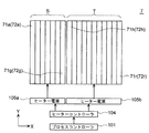
【解決手段】 加熱処理装置28は、基板Gを一方向に搬送する搬送路としてのコロ搬送機構5と、搬送路を囲繞するように設けられたケーシング6と、ケーシング6内に搬送路を搬送される基板Gの両面側に、基板Gに近接するように搬送路に沿ってそれぞれ設けられた第1および第2の面状ヒーター71a〜71r、72a〜72rとを具備する。
【選択図】 図3
Description
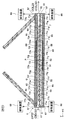
図1は、本発明の一実施形態に係る加熱処理装置が搭載された、FPD用のガラス基板(以下、単に「基板」と記す)へのレジスト膜の形成および露光処理後のレジスト膜の現像処理を行うレジスト塗布・現像処理システムの概略平面図である。
図2は加熱処理ユニット(HT)28(加熱処理装置)を示す平面方向の断面図であり、図3はその側面方向の断面図である。
図7は第1および第2の面状ヒーター71、72の制御系の他の例を示す概念図である。
5…コロ搬送機構
6…ケーシング
50…コロ部材
52…外周面部
63…内壁
64…外壁
65…空間
71(71a〜71r)…第1の面状ヒーター
72(72a〜72r)…第2の面状ヒーター
G…基板
Claims (9)
- 基板に加熱処理を施す加熱処理装置であって、
基板を一方向に搬送する搬送路と、
前記搬送路を囲繞するように設けられたケーシングと、
前記搬送路に沿って前記ケーシング内に、前記搬送路を搬送される基板に近接するように基板の両面側にそれぞれ設けられた第1および第2の面状ヒーターと
を具備することを特徴とする加熱処理装置。 - 前記搬送路は、一方向に間隔をあけて複数設けられたコロ部材の回転によって基板をコロ搬送し、
前記第1の面状ヒーターは、前記コロ部材同士の間にそれぞれ設けられて搬送方向に複数配列されていることを特徴とする請求項1に記載の加熱処理装置。 - 前記第2の面状ヒーターは、前記第1の面状ヒーターの配列ピッチと対応するように搬送方向に複数配列され、
前記複数の第1および第2の面状ヒーターは、個別または搬送方向に区分けされたグループごとに温度制御可能であることを特徴とする請求項2に記載の加熱処理装置。 - 前記複数の第1および第2の面状ヒーターが、個別または搬送方向に区分けされたグループごとに温度制御されることにより、前記複数の第1および第2の面状ヒーターからなるヒーター群は所定の温度プロファイルを形成することを特徴とする請求項3に記載の加熱処理装置。
- 前記第1および第2の面状ヒーターはそれぞれ、前記搬送路の幅方向に複数に区分けされた領域ごとに温度制御可能であることを特徴とする請求項3または請求項4に記載の加熱処理装置。
- 前記第2の面状ヒーターは、前記ケーシングの一壁部に取り付けられており、
前記ケーシングの前記一壁部は、前記ケーシング内を開閉する扉として機能することを特徴とする請求項3から請求項5のいずれか1項に記載の加熱処理装置。 - 前記コロ部材は、少なくとも外周面が熱伝導率の低い材料からなることを特徴とする請求項2から請求項6のいずれか1項に記載の加熱処理装置。
- 前記ケーシングの壁部の少なくとも一部は、互いに空間をあけて設けられた内壁および外壁を備えた二重壁構造を有しており、前記内壁および外壁の間の空間が前記ケーシング内外を断熱する空気断熱層として機能することを特徴とする請求項1から請求項7のいずれか1項に記載の加熱処理装置。
- 前記搬送路を搬送される基板の搬送経路と前記第1および第2の面状ヒーターとの間隔はそれぞれ、5〜30mmであることを特徴とする請求項1から請求項8のいずれか1項に記載の加熱処理装置。
Priority Applications (4)
| Application Number | Priority Date | Filing Date | Title |
|---|---|---|---|
| JP2005355183A JP4531690B2 (ja) | 2005-12-08 | 2005-12-08 | 加熱処理装置 |
| KR1020060123948A KR101269748B1 (ko) | 2005-12-08 | 2006-12-07 | 가열 처리 장치 |
| TW095145644A TWI339872B (en) | 2005-12-08 | 2006-12-07 | Heat treatment unit |
| CNB2006101656028A CN100474507C (zh) | 2005-12-08 | 2006-12-08 | 加热处理装置 |
Applications Claiming Priority (1)
| Application Number | Priority Date | Filing Date | Title |
|---|---|---|---|
| JP2005355183A JP4531690B2 (ja) | 2005-12-08 | 2005-12-08 | 加熱処理装置 |
Publications (2)
| Publication Number | Publication Date |
|---|---|
| JP2007158253A true JP2007158253A (ja) | 2007-06-21 |
| JP4531690B2 JP4531690B2 (ja) | 2010-08-25 |
Family
ID=38130875
Family Applications (1)
| Application Number | Title | Priority Date | Filing Date |
|---|---|---|---|
| JP2005355183A Expired - Fee Related JP4531690B2 (ja) | 2005-12-08 | 2005-12-08 | 加熱処理装置 |
Country Status (4)
| Country | Link |
|---|---|
| JP (1) | JP4531690B2 (ja) |
| KR (1) | KR101269748B1 (ja) |
| CN (1) | CN100474507C (ja) |
| TW (1) | TWI339872B (ja) |
Cited By (11)
| Publication number | Priority date | Publication date | Assignee | Title |
|---|---|---|---|---|
| JP2011066318A (ja) * | 2009-09-18 | 2011-03-31 | Tokyo Electron Ltd | 熱処理装置 |
| JP2011216572A (ja) * | 2010-03-31 | 2011-10-27 | Dainippon Screen Mfg Co Ltd | 基板処理装置 |
| KR20120002428A (ko) | 2010-06-30 | 2012-01-05 | 도쿄엘렉트론가부시키가이샤 | 국소 노광 장치, 국소 노광 방법 및 기억 매체 |
| KR20120071347A (ko) | 2010-12-22 | 2012-07-02 | 도쿄엘렉트론가부시키가이샤 | 국소 노광 방법 및 국소 노광 장치 |
| JP2012182308A (ja) * | 2011-03-01 | 2012-09-20 | Tokyo Electron Ltd | 浮上式塗布装置 |
| KR20120105374A (ko) | 2011-03-15 | 2012-09-25 | 도쿄엘렉트론가부시키가이샤 | 국소 노광 방법 및 국소 노광 장치 |
| JP2013061081A (ja) * | 2011-09-12 | 2013-04-04 | Dainippon Screen Mfg Co Ltd | 熱処理装置 |
| JP2020035884A (ja) * | 2018-08-30 | 2020-03-05 | 東京エレクトロン株式会社 | 基板処理装置および基板処理方法 |
| JP2020035935A (ja) * | 2018-08-30 | 2020-03-05 | 東京エレクトロン株式会社 | 基板処理装置および基板処理方法 |
| CN111383975A (zh) * | 2018-12-27 | 2020-07-07 | 东京毅力科创株式会社 | 基片处理装置和基片处理方法 |
| KR20200081256A (ko) | 2018-12-27 | 2020-07-07 | 도쿄엘렉트론가부시키가이샤 | 기판 처리 장치 및 기판 처리 방법 |
Families Citing this family (5)
| Publication number | Priority date | Publication date | Assignee | Title |
|---|---|---|---|---|
| KR101055862B1 (ko) * | 2009-03-23 | 2011-08-09 | 주식회사 테라세미콘 | 인라인 열처리 장치 |
| JP5226037B2 (ja) * | 2010-06-04 | 2013-07-03 | 東京エレクトロン株式会社 | 熱処理装置及び熱処理方法 |
| JP7265314B2 (ja) * | 2017-03-03 | 2023-04-26 | 株式会社Screenホールディングス | 熱処理方法および熱処理装置 |
| US11476167B2 (en) | 2017-03-03 | 2022-10-18 | SCREEN Holdings Co., Ltd. | Heat treatment method and heat treatment apparatus of light irradiation type |
| KR102220853B1 (ko) * | 2019-05-27 | 2021-02-26 | 주식회사 선코리아 | 열처리장치 |
Citations (9)
| Publication number | Priority date | Publication date | Assignee | Title |
|---|---|---|---|---|
| JPS62252989A (ja) * | 1986-04-25 | 1987-11-04 | 日本電気株式会社 | 印刷配線板の製造方法 |
| JPH0193121A (ja) * | 1987-10-05 | 1989-04-12 | Kawasaki Steel Corp | 半導体ウェハベーキング装置 |
| JPH0270426A (ja) * | 1988-09-06 | 1990-03-09 | Kawasaki Steel Corp | 制振性を備えた複合鋼板 |
| JPH04243119A (ja) * | 1991-01-17 | 1992-08-31 | Sharp Corp | レジスト加熱装置 |
| JPH0531223U (ja) * | 1991-09-30 | 1993-04-23 | 日本電気株式会社 | 液晶デイスプレイアクテイブ素子製造用現像装置 |
| JPH0845817A (ja) * | 1994-07-28 | 1996-02-16 | Fujitsu Ltd | ベーキング装置 |
| JPH0953881A (ja) * | 1995-08-11 | 1997-02-25 | Fuji Photo Film Co Ltd | 硬基板のベーク装置 |
| JPH09310198A (ja) * | 1996-05-20 | 1997-12-02 | Dainippon Printing Co Ltd | 電着レジスト乾燥装置 |
| JPH1147668A (ja) * | 1997-06-06 | 1999-02-23 | Kansai Denshi Kk | 基板乾燥装置 |
Family Cites Families (1)
| Publication number | Priority date | Publication date | Assignee | Title |
|---|---|---|---|---|
| JP2005123284A (ja) * | 2003-10-15 | 2005-05-12 | Renesas Technology Corp | 半導体製造装置 |
-
2005
- 2005-12-08 JP JP2005355183A patent/JP4531690B2/ja not_active Expired - Fee Related
-
2006
- 2006-12-07 TW TW095145644A patent/TWI339872B/zh not_active IP Right Cessation
- 2006-12-07 KR KR1020060123948A patent/KR101269748B1/ko not_active Expired - Fee Related
- 2006-12-08 CN CNB2006101656028A patent/CN100474507C/zh not_active Expired - Fee Related
Patent Citations (9)
| Publication number | Priority date | Publication date | Assignee | Title |
|---|---|---|---|---|
| JPS62252989A (ja) * | 1986-04-25 | 1987-11-04 | 日本電気株式会社 | 印刷配線板の製造方法 |
| JPH0193121A (ja) * | 1987-10-05 | 1989-04-12 | Kawasaki Steel Corp | 半導体ウェハベーキング装置 |
| JPH0270426A (ja) * | 1988-09-06 | 1990-03-09 | Kawasaki Steel Corp | 制振性を備えた複合鋼板 |
| JPH04243119A (ja) * | 1991-01-17 | 1992-08-31 | Sharp Corp | レジスト加熱装置 |
| JPH0531223U (ja) * | 1991-09-30 | 1993-04-23 | 日本電気株式会社 | 液晶デイスプレイアクテイブ素子製造用現像装置 |
| JPH0845817A (ja) * | 1994-07-28 | 1996-02-16 | Fujitsu Ltd | ベーキング装置 |
| JPH0953881A (ja) * | 1995-08-11 | 1997-02-25 | Fuji Photo Film Co Ltd | 硬基板のベーク装置 |
| JPH09310198A (ja) * | 1996-05-20 | 1997-12-02 | Dainippon Printing Co Ltd | 電着レジスト乾燥装置 |
| JPH1147668A (ja) * | 1997-06-06 | 1999-02-23 | Kansai Denshi Kk | 基板乾燥装置 |
Cited By (18)
| Publication number | Priority date | Publication date | Assignee | Title |
|---|---|---|---|---|
| JP2011066318A (ja) * | 2009-09-18 | 2011-03-31 | Tokyo Electron Ltd | 熱処理装置 |
| JP2011216572A (ja) * | 2010-03-31 | 2011-10-27 | Dainippon Screen Mfg Co Ltd | 基板処理装置 |
| KR20120002428A (ko) | 2010-06-30 | 2012-01-05 | 도쿄엘렉트론가부시키가이샤 | 국소 노광 장치, 국소 노광 방법 및 기억 매체 |
| US9146481B2 (en) | 2010-06-30 | 2015-09-29 | Tokyo Electron Limited | Local exposure apparatus, local exposure method and storage medium |
| US8691481B2 (en) | 2010-12-22 | 2014-04-08 | Tokyo Electron Limited | Local exposure method and local exposure apparatus |
| KR20120071347A (ko) | 2010-12-22 | 2012-07-02 | 도쿄엘렉트론가부시키가이샤 | 국소 노광 방법 및 국소 노광 장치 |
| JP2012182308A (ja) * | 2011-03-01 | 2012-09-20 | Tokyo Electron Ltd | 浮上式塗布装置 |
| KR20120105374A (ko) | 2011-03-15 | 2012-09-25 | 도쿄엘렉트론가부시키가이샤 | 국소 노광 방법 및 국소 노광 장치 |
| JP2013061081A (ja) * | 2011-09-12 | 2013-04-04 | Dainippon Screen Mfg Co Ltd | 熱処理装置 |
| JP2020035884A (ja) * | 2018-08-30 | 2020-03-05 | 東京エレクトロン株式会社 | 基板処理装置および基板処理方法 |
| JP2020035935A (ja) * | 2018-08-30 | 2020-03-05 | 東京エレクトロン株式会社 | 基板処理装置および基板処理方法 |
| KR20200026085A (ko) | 2018-08-30 | 2020-03-10 | 도쿄엘렉트론가부시키가이샤 | 기판 처리 장치 및 기판 처리 방법 |
| KR20200026084A (ko) | 2018-08-30 | 2020-03-10 | 도쿄엘렉트론가부시키가이샤 | 기판 처리 장치 및 기판 처리 방법 |
| JP7232593B2 (ja) | 2018-08-30 | 2023-03-03 | 東京エレクトロン株式会社 | 基板処理装置および基板処理方法 |
| JP7232596B2 (ja) | 2018-08-30 | 2023-03-03 | 東京エレクトロン株式会社 | 基板処理装置および基板処理方法 |
| CN111383975A (zh) * | 2018-12-27 | 2020-07-07 | 东京毅力科创株式会社 | 基片处理装置和基片处理方法 |
| KR20200081257A (ko) | 2018-12-27 | 2020-07-07 | 도쿄엘렉트론가부시키가이샤 | 기판 처리 장치 및 기판 처리 방법 |
| KR20200081256A (ko) | 2018-12-27 | 2020-07-07 | 도쿄엘렉트론가부시키가이샤 | 기판 처리 장치 및 기판 처리 방법 |
Also Published As
| Publication number | Publication date |
|---|---|
| CN100474507C (zh) | 2009-04-01 |
| TW200737393A (en) | 2007-10-01 |
| KR101269748B1 (ko) | 2013-05-30 |
| CN1979765A (zh) | 2007-06-13 |
| JP4531690B2 (ja) | 2010-08-25 |
| TWI339872B (en) | 2011-04-01 |
| KR20070061418A (ko) | 2007-06-13 |
Similar Documents
| Publication | Publication Date | Title |
|---|---|---|
| JP4531690B2 (ja) | 加熱処理装置 | |
| JP4542577B2 (ja) | 常圧乾燥装置及び基板処理装置及び基板処理方法 | |
| CN100521078C (zh) | 基板冷却装置、基板冷却方法 | |
| JP4341978B2 (ja) | 基板処理装置 | |
| JP4592787B2 (ja) | 基板処理装置 | |
| JP4384686B2 (ja) | 常圧乾燥装置及び基板処理装置及び基板処理方法 | |
| JP4672538B2 (ja) | 加熱処理装置 | |
| JP5377463B2 (ja) | 加熱処理装置 | |
| CN100505155C (zh) | 基板冷却装置 | |
| KR20080060165A (ko) | 기판 처리 장치 | |
| JP4319175B2 (ja) | 減圧乾燥装置 | |
| TWI797325B (zh) | 基板處理裝置及基板處理方法 | |
| JP4967013B2 (ja) | 基板処理装置、基板処理方法及びこの基板処理方法を実行させるためのプログラムを記録した記録媒体 | |
| JP4005609B2 (ja) | 基板処理装置及び基板処理方法並びに基板の製造方法 | |
| JP4015015B2 (ja) | 熱処理装置 | |
| JP3576826B2 (ja) | 加熱処理装置および加熱処理方法 | |
| JP4472647B2 (ja) | 加熱処理装置、加熱処理方法、コンピュータ読取可能な記憶媒体 | |
| JP3966884B2 (ja) | 基板処理装置及び基板処理方法並びに基板の製造方法 | |
| JP2008124502A (ja) | 基板処理装置及び基板処理方法及び基板の製造方法及び電子機器 |
Legal Events
| Date | Code | Title | Description |
|---|---|---|---|
| A621 | Written request for application examination |
Free format text: JAPANESE INTERMEDIATE CODE: A621 Effective date: 20070903 |
|
| A131 | Notification of reasons for refusal |
Free format text: JAPANESE INTERMEDIATE CODE: A131 Effective date: 20091222 |
|
| A521 | Request for written amendment filed |
Free format text: JAPANESE INTERMEDIATE CODE: A523 Effective date: 20100219 |
|
| TRDD | Decision of grant or rejection written | ||
| A01 | Written decision to grant a patent or to grant a registration (utility model) |
Free format text: JAPANESE INTERMEDIATE CODE: A01 Effective date: 20100608 |
|
| A01 | Written decision to grant a patent or to grant a registration (utility model) |
Free format text: JAPANESE INTERMEDIATE CODE: A01 |
|
| A61 | First payment of annual fees (during grant procedure) |
Free format text: JAPANESE INTERMEDIATE CODE: A61 Effective date: 20100609 |
|
| R150 | Certificate of patent or registration of utility model |
Ref document number: 4531690 Country of ref document: JP Free format text: JAPANESE INTERMEDIATE CODE: R150 Free format text: JAPANESE INTERMEDIATE CODE: R150 |
|
| FPAY | Renewal fee payment (event date is renewal date of database) |
Free format text: PAYMENT UNTIL: 20130618 Year of fee payment: 3 |
|
| R250 | Receipt of annual fees |
Free format text: JAPANESE INTERMEDIATE CODE: R250 |
|
| R250 | Receipt of annual fees |
Free format text: JAPANESE INTERMEDIATE CODE: R250 |
|
| R250 | Receipt of annual fees |
Free format text: JAPANESE INTERMEDIATE CODE: R250 |
|
| R250 | Receipt of annual fees |
Free format text: JAPANESE INTERMEDIATE CODE: R250 |
|
| R250 | Receipt of annual fees |
Free format text: JAPANESE INTERMEDIATE CODE: R250 |
|
| R250 | Receipt of annual fees |
Free format text: JAPANESE INTERMEDIATE CODE: R250 |
|
| R250 | Receipt of annual fees |
Free format text: JAPANESE INTERMEDIATE CODE: R250 |
|
| LAPS | Cancellation because of no payment of annual fees |