JP2007304151A - 液晶表示素子、電子機器、および液晶表示素子の製造方法 - Google Patents
液晶表示素子、電子機器、および液晶表示素子の製造方法 Download PDFInfo
- Publication number
- JP2007304151A JP2007304151A JP2006129830A JP2006129830A JP2007304151A JP 2007304151 A JP2007304151 A JP 2007304151A JP 2006129830 A JP2006129830 A JP 2006129830A JP 2006129830 A JP2006129830 A JP 2006129830A JP 2007304151 A JP2007304151 A JP 2007304151A
- Authority
- JP
- Japan
- Prior art keywords
- liquid crystal
- layer
- hybrid
- display element
- retardation layer
- Prior art date
- Legal status (The legal status is an assumption and is not a legal conclusion. Google has not performed a legal analysis and makes no representation as to the accuracy of the status listed.)
- Granted
Links
Images


Classifications
-
- G—PHYSICS
- G02—OPTICS
- G02F—OPTICAL DEVICES OR ARRANGEMENTS FOR THE CONTROL OF LIGHT BY MODIFICATION OF THE OPTICAL PROPERTIES OF THE MEDIA OF THE ELEMENTS INVOLVED THEREIN; NON-LINEAR OPTICS; FREQUENCY-CHANGING OF LIGHT; OPTICAL LOGIC ELEMENTS; OPTICAL ANALOGUE/DIGITAL CONVERTERS
- G02F1/00—Devices or arrangements for the control of the intensity, colour, phase, polarisation or direction of light arriving from an independent light source, e.g. switching, gating or modulating; Non-linear optics
- G02F1/01—Devices or arrangements for the control of the intensity, colour, phase, polarisation or direction of light arriving from an independent light source, e.g. switching, gating or modulating; Non-linear optics for the control of the intensity, phase, polarisation or colour
- G02F1/13—Devices or arrangements for the control of the intensity, colour, phase, polarisation or direction of light arriving from an independent light source, e.g. switching, gating or modulating; Non-linear optics for the control of the intensity, phase, polarisation or colour based on liquid crystals, e.g. single liquid crystal display cells
- G02F1/133—Constructional arrangements; Operation of liquid crystal cells; Circuit arrangements
- G02F1/1333—Constructional arrangements; Manufacturing methods
- G02F1/1335—Structural association of cells with optical devices, e.g. polarisers or reflectors
- G02F1/13363—Birefringent elements, e.g. for optical compensation
- G02F1/133632—Birefringent elements, e.g. for optical compensation with refractive index ellipsoid inclined relative to the LC-layer surface
-
- G—PHYSICS
- G02—OPTICS
- G02F—OPTICAL DEVICES OR ARRANGEMENTS FOR THE CONTROL OF LIGHT BY MODIFICATION OF THE OPTICAL PROPERTIES OF THE MEDIA OF THE ELEMENTS INVOLVED THEREIN; NON-LINEAR OPTICS; FREQUENCY-CHANGING OF LIGHT; OPTICAL LOGIC ELEMENTS; OPTICAL ANALOGUE/DIGITAL CONVERTERS
- G02F1/00—Devices or arrangements for the control of the intensity, colour, phase, polarisation or direction of light arriving from an independent light source, e.g. switching, gating or modulating; Non-linear optics
- G02F1/01—Devices or arrangements for the control of the intensity, colour, phase, polarisation or direction of light arriving from an independent light source, e.g. switching, gating or modulating; Non-linear optics for the control of the intensity, phase, polarisation or colour
- G02F1/13—Devices or arrangements for the control of the intensity, colour, phase, polarisation or direction of light arriving from an independent light source, e.g. switching, gating or modulating; Non-linear optics for the control of the intensity, phase, polarisation or colour based on liquid crystals, e.g. single liquid crystal display cells
- G02F1/133—Constructional arrangements; Operation of liquid crystal cells; Circuit arrangements
- G02F1/1333—Constructional arrangements; Manufacturing methods
- G02F1/1335—Structural association of cells with optical devices, e.g. polarisers or reflectors
- G02F1/13363—Birefringent elements, e.g. for optical compensation
-
- G—PHYSICS
- G02—OPTICS
- G02F—OPTICAL DEVICES OR ARRANGEMENTS FOR THE CONTROL OF LIGHT BY MODIFICATION OF THE OPTICAL PROPERTIES OF THE MEDIA OF THE ELEMENTS INVOLVED THEREIN; NON-LINEAR OPTICS; FREQUENCY-CHANGING OF LIGHT; OPTICAL LOGIC ELEMENTS; OPTICAL ANALOGUE/DIGITAL CONVERTERS
- G02F1/00—Devices or arrangements for the control of the intensity, colour, phase, polarisation or direction of light arriving from an independent light source, e.g. switching, gating or modulating; Non-linear optics
- G02F1/01—Devices or arrangements for the control of the intensity, colour, phase, polarisation or direction of light arriving from an independent light source, e.g. switching, gating or modulating; Non-linear optics for the control of the intensity, phase, polarisation or colour
- G02F1/13—Devices or arrangements for the control of the intensity, colour, phase, polarisation or direction of light arriving from an independent light source, e.g. switching, gating or modulating; Non-linear optics for the control of the intensity, phase, polarisation or colour based on liquid crystals, e.g. single liquid crystal display cells
- G02F1/133—Constructional arrangements; Operation of liquid crystal cells; Circuit arrangements
- G02F1/1333—Constructional arrangements; Manufacturing methods
- G02F1/1335—Structural association of cells with optical devices, e.g. polarisers or reflectors
- G02F1/13356—Structural association of cells with optical devices, e.g. polarisers or reflectors characterised by the placement of the optical elements
- G02F1/133565—Structural association of cells with optical devices, e.g. polarisers or reflectors characterised by the placement of the optical elements inside the LC elements, i.e. between the cell substrates
-
- G—PHYSICS
- G02—OPTICS
- G02F—OPTICAL DEVICES OR ARRANGEMENTS FOR THE CONTROL OF LIGHT BY MODIFICATION OF THE OPTICAL PROPERTIES OF THE MEDIA OF THE ELEMENTS INVOLVED THEREIN; NON-LINEAR OPTICS; FREQUENCY-CHANGING OF LIGHT; OPTICAL LOGIC ELEMENTS; OPTICAL ANALOGUE/DIGITAL CONVERTERS
- G02F1/00—Devices or arrangements for the control of the intensity, colour, phase, polarisation or direction of light arriving from an independent light source, e.g. switching, gating or modulating; Non-linear optics
- G02F1/01—Devices or arrangements for the control of the intensity, colour, phase, polarisation or direction of light arriving from an independent light source, e.g. switching, gating or modulating; Non-linear optics for the control of the intensity, phase, polarisation or colour
- G02F1/13—Devices or arrangements for the control of the intensity, colour, phase, polarisation or direction of light arriving from an independent light source, e.g. switching, gating or modulating; Non-linear optics for the control of the intensity, phase, polarisation or colour based on liquid crystals, e.g. single liquid crystal display cells
- G02F1/133—Constructional arrangements; Operation of liquid crystal cells; Circuit arrangements
- G02F1/1333—Constructional arrangements; Manufacturing methods
- G02F1/1335—Structural association of cells with optical devices, e.g. polarisers or reflectors
- G02F1/13363—Birefringent elements, e.g. for optical compensation
- G02F1/133631—Birefringent elements, e.g. for optical compensation with a spatial distribution of the retardation value
-
- G—PHYSICS
- G02—OPTICS
- G02F—OPTICAL DEVICES OR ARRANGEMENTS FOR THE CONTROL OF LIGHT BY MODIFICATION OF THE OPTICAL PROPERTIES OF THE MEDIA OF THE ELEMENTS INVOLVED THEREIN; NON-LINEAR OPTICS; FREQUENCY-CHANGING OF LIGHT; OPTICAL LOGIC ELEMENTS; OPTICAL ANALOGUE/DIGITAL CONVERTERS
- G02F2413/00—Indexing scheme related to G02F1/13363, i.e. to birefringent elements, e.g. for optical compensation, characterised by the number, position, orientation or value of the compensation plates
- G02F2413/10—Indexing scheme related to G02F1/13363, i.e. to birefringent elements, e.g. for optical compensation, characterised by the number, position, orientation or value of the compensation plates with refractive index ellipsoid inclined, or tilted, relative to the LC-layer surface O plate
- G02F2413/105—Indexing scheme related to G02F1/13363, i.e. to birefringent elements, e.g. for optical compensation, characterised by the number, position, orientation or value of the compensation plates with refractive index ellipsoid inclined, or tilted, relative to the LC-layer surface O plate with varying inclination in thickness direction, e.g. hybrid oriented discotic LC
Landscapes
- Physics & Mathematics (AREA)
- Nonlinear Science (AREA)
- Mathematical Physics (AREA)
- Chemical & Material Sciences (AREA)
- Crystallography & Structural Chemistry (AREA)
- General Physics & Mathematics (AREA)
- Optics & Photonics (AREA)
- Liquid Crystal (AREA)
- Polarising Elements (AREA)
- Optical Filters (AREA)
Abstract
【解決手段】一対の透明基板11−21間に液晶層LCを狭持してなる液晶セルと、液晶分子をハイブリッド配向させたハイブリッド位相差層23とを組み合わせた電界複屈折モードの液晶表示素子1aにおいて、ハイブリッド位相差層23は、一対の透明基板11,21のうちの一方の対向基板20側の透明基板21における液晶層LC側に成膜形成されたものとする。
【選択図】図1
Description
図1は第1実施形態の液晶表示素子1aの断面構成図である。この図に示す液晶表示素子1aは、液晶分子をハイブリッド配向させた位相差層(以下ハイブリッド位相差層と記す)を備え、ECBモードで駆動される透過型の液晶表示素子1aであり、次のように構成されている。
図5は第2実施形態の液晶表示素子1bの断面構成図である。この図に示す液晶表示装置1bが、図1を用いて説明した第1実施形態の液晶表示素子と異なるところは、λ/4位相差層30が対向基板20側に設けられているところにあり、他の構成は第1実施形態と同様であることとする。
図7は第3実施形態の液晶表示素子1cの断面構成図である。この図に示す液晶表示装置1cが、図1を用いて説明した液晶表示素子と異なるところは、ハイブリッド位相差層23と共にλ/4位相差層30’が、対向基板20における液晶層LC側に設けられているところにあり、他の構成は第1実施形態と同様であることとする。
図9は第4実施形態の液晶表示素子1dの断面構成図である。ここでは、半透過型の液晶表示素子に本発明を適用した実施の形態を説明する。この図に示す液晶表示素子1dは、液晶分子をハイブリッド配向させた位相差層(以下ハイブリッド位相差層と記す)を備え、ECBモードで駆動される半透過型の液晶表示素子1dであり、次のように構成されている。
図10は第5実施形態の液晶表示素子1eの断面構成図である。この図に示す液晶表示装置1eが、図9を用いて説明した第4実施形態の液晶表示素子と異なるところは、ハイブリッド位相差層23と共にλ/2位相差層43’が、対向基板20における液晶層LC側に設けられているところにあり、他の構成は第4実施形態と同様であることとする。
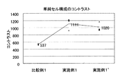
図11には、駆動素子を設けていない単純構成として、透明基板における液晶層側にハイブリッド位相差層を成膜形成した透過型の液晶表示素子(実施例1,1’)のコントラストと、フィルム状のハイブリッド位相差層を透明基板の外側に貼り合わせた透過型の液晶表示素子(比較例1)のコントラストとを示す。尚、実施例1,1’は同一構成で、異なるロットの素子であることとする。
図12には、駆動素子を設けたアクティブ構成として、透明基板における液晶層側にハイブリッド位相差層を成膜形成した透過型の液晶表示素子(実施例2)のコントラストと、フィルム状のハイブリッド位相差層を透明基板の外側に貼り合わせた透過型の液晶表示素子(比較例2)のコントラストとを示す。
図14には、ハイブリッド位相差層とECBモードの液晶セルとを組み合わせた構成の透過型の液晶表示素子についての視野角特性を示す。図14(1)は、ハイブリッド位相差層の配向方向と、このハイブリッド位相差層側における液晶層の配向方向とを、180°の反平行とした構成の液晶表示素子の視野角特性である。一方、図14(2)は、ハイブリッド位相差層の配向方向と、このハイブリッド位相差層側における液晶層の配向方向とを、0°の平行とした構成の液晶表示素子の視野角特性である。尚、図中の白線は、コントラスト10を示す。
図15(1)には、フィルム基材上に成膜形成されたハイブリッド位相差層の光学写真を示す。一方、図15(2)には、ガラスからなる透明基板上に成膜形成されたハイブリッド位相差層の光学写真を示す。これらの光学写真を比較し、図15(1)のフィルム基材上に成膜形成されたハイブリッド位相差層では、配向不良が発生して白点として観察されるのに対して、図15(2)のガラスからなる透明基板上に成膜形成されたハイブリッド位相差層では白点が観察されず、配向不良のないハイブリッド位相差層が形成さることが確認された。
Claims (14)
- 一対の基板間に液晶層を狭持してなる液晶セルと、液晶分子をハイブリッド配向させたハイブリッド位相差層とを組み合わせた電界複屈折モードの液晶表示素子において、
前記ハイブリッド位相差層は、前記一対の基板のうちの一方の基板における前記液晶層側に成膜形成されたものである
ことを特徴とする液晶表示素子。 - 請求項1記載の液晶表示素子において、
前記ハイブリッド位相差層を構成する液晶分子が正の屈折率異方性を有する
ことを特徴とする液晶表示素子。 - 請求項1記載の液晶表示素子において、
前記一対の基板のうちの他方の基板には、画素電極とこれを駆動する駆動素子が設けられている
ことを特徴とする液晶表示素子。 - 請求項1記載の液晶表示素子において、
前記ハイブリッド位相差層の配向方向と当該ハイブリッド位相差層側における前記液晶層の配向方向とが、150°以上、210°以下の角度をなしている
ことを特徴とする液晶表示素子。 - 請求項1記載の液晶表示素子において、
前記液晶セルの外側または前記ハイブリッド位相差層と前記一方の基板との間に、λ/4位相差層が設けられている
ことを特徴とする液晶表示素子。 - 請求項5記載の液晶表示素子において、
前記ハイブリッド位相差層の配向軸と、前記λ/4位相差層の光軸とが80°以上、100°以下の角度をなしている
ことを特徴とする液晶表示素子。 - 請求項5記載の液晶表示素子において、
前記ハイブリッド位相差層の位相差と電圧無印加時の白表示における前記液晶層の位相差との合計から、前記λ/4位相差層の位相差を引いた位相差がλ/2となり、
前記ハイブリッド位相差層の位相差と電圧印加時の黒表示における前記液晶層の位相差との合計から、前記λ/4位相差層の位相差を引いた位相差が0となる
ことを特徴とする液晶表示素子 - 請求項1記載の液晶表示素子において、
前記ハイブリッド位相差層の位相差と、電圧無印加時における前記液晶層の位相差との合計が、(3/4)λであり、
前記ハイブリッド位相差層の位相差と、電圧印加時における前記液晶層の位相差との合計が、(1/4)λである
ことを特徴とする液晶表示素子。 - 請求項1記載の液晶表示素子において、
前記ハイブリッド位相差層の液晶側または当該ハイブリッド位相差層と前記一方の基板との間には、カラーフィルタが設けられている
ことを特徴とする液晶表示素子。 - 請求項1記載の液晶表示素子において、
前記ハイブリッド位相差層を構成する液晶分子は、ネマチック液晶にアクリレート基がついた分子構造である
ことを特徴とする液晶表示素子。 - 請求項1記載の液晶表示素子において、
前記液晶セルは、画素毎に反射表示領域と透過表示領域とを備えた
ことを特徴とする液晶表示素子。 - 一対の基板間に液晶層を狭持してなる液晶セルと、液晶分子をハイブリッド配向させたハイブリッド位相差層とを組み合わせた電界複屈折モードの液晶表示素子を備えた電子機器において、
前記ハイブリッド位相差層は、前記一対の基板のうちの一方の基板における液晶層側に成膜形成されたものである
ことを特徴とする電子機器。 - 液晶分子をハイブリッド配向させたハイブリッド位相差層を第1の基板上に形成する工程と、前記第1の基板における前記ハイブリッド位相差層の形成面側に対向配置した第2の基板との間に液晶層を充填封止する工程とを行う液晶表示素子の製造方法であって、
前記ハイブリッド位相差層を成膜形成する工程では、
前記第1の基板上に配向膜を介して光硬化性液晶を用いたハイブリッド位相差層の材料膜を成膜し、
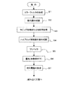
前記材料膜の加熱温度によって位相差の視野角依存性を制御しながら当該材料膜に対して露光を行うことにより、当該材料膜を硬化させたハイブリッド位相差層を成膜形成する
ことを特徴とする液晶表示素子の製造方法。 - 液晶分子をハイブリッド配向させたハイブリッド位相差層を第1の基板上に形成する工程と、前記第1の基板における前記ハイブリッド位相差層の形成面側に対向配置した第2の基板との間に液晶層を充填封止する工程とを行う液晶表示素子の製造方法であって、
前記ハイブリッド位相差層を成膜形成する工程では、
前記第1の基板上に配向膜を介して光硬化性液晶を用いたハイブリッド位相差層の材料膜を成膜し、
露光によって前記材料膜を硬化させたハイブリッド位相差層を成膜形成し、
前記ハイブリッド位相差層の表面層を所定膜厚で除去することにより、当該ハイブリッド位相差層における位相差の視野角依存性を制御する
ことを特徴とする液晶表示素子の製造方法。
Priority Applications (5)
| Application Number | Priority Date | Filing Date | Title |
|---|---|---|---|
| JP2006129830A JP4868219B2 (ja) | 2006-05-09 | 2006-05-09 | 液晶表示素子、電子機器、および液晶表示素子の製造方法 |
| TW096115065A TW200809348A (en) | 2006-05-09 | 2007-04-27 | Liquid crystal display element, electronic device, and manufacturing method of liquid crystal display element |
| US11/743,977 US7659954B2 (en) | 2006-05-09 | 2007-05-03 | Liquid crystal display device, electronic equipment, and method of manufacturing liquid crystal display device |
| KR1020070043679A KR101278089B1 (ko) | 2006-05-09 | 2007-05-04 | 액정 표시 소자, 전자 기기 및 액정 표시 소자의 제조 방법 |
| CN2007101421421A CN101114083B (zh) | 2006-05-09 | 2007-05-09 | 液晶显示元件、电子设备及液晶显示元件的制造方法 |
Applications Claiming Priority (1)
| Application Number | Priority Date | Filing Date | Title |
|---|---|---|---|
| JP2006129830A JP4868219B2 (ja) | 2006-05-09 | 2006-05-09 | 液晶表示素子、電子機器、および液晶表示素子の製造方法 |
Publications (3)
| Publication Number | Publication Date |
|---|---|
| JP2007304151A true JP2007304151A (ja) | 2007-11-22 |
| JP2007304151A5 JP2007304151A5 (ja) | 2009-04-02 |
| JP4868219B2 JP4868219B2 (ja) | 2012-02-01 |
Family
ID=38838147
Family Applications (1)
| Application Number | Title | Priority Date | Filing Date |
|---|---|---|---|
| JP2006129830A Active JP4868219B2 (ja) | 2006-05-09 | 2006-05-09 | 液晶表示素子、電子機器、および液晶表示素子の製造方法 |
Country Status (5)
| Country | Link |
|---|---|
| US (1) | US7659954B2 (ja) |
| JP (1) | JP4868219B2 (ja) |
| KR (1) | KR101278089B1 (ja) |
| CN (1) | CN101114083B (ja) |
| TW (1) | TW200809348A (ja) |
Cited By (2)
| Publication number | Priority date | Publication date | Assignee | Title |
|---|---|---|---|---|
| JP2008203382A (ja) * | 2007-02-19 | 2008-09-04 | Hitachi Displays Ltd | 液晶表示装置 |
| WO2018180851A1 (ja) * | 2017-03-28 | 2018-10-04 | シャープ株式会社 | 液晶表示装置、及び、液晶表示装置の製造方法 |
Families Citing this family (3)
| Publication number | Priority date | Publication date | Assignee | Title |
|---|---|---|---|---|
| TWI420196B (zh) * | 2008-12-11 | 2013-12-21 | Au Optronics Corp | 液晶顯示器 |
| DE102011056836B4 (de) * | 2011-06-22 | 2020-12-24 | Lg Display Co., Ltd. | Organische lichtemittierende Anzeigevorrichtung |
| JP7810009B2 (ja) * | 2022-02-25 | 2026-02-03 | セイコーエプソン株式会社 | 液晶装置、表示装置、光変調モジュール、および液晶装置の制御方法 |
Citations (4)
| Publication number | Priority date | Publication date | Assignee | Title |
|---|---|---|---|---|
| JP2003287753A (ja) * | 2002-01-28 | 2003-10-10 | Fujitsu Display Technologies Corp | 液晶表示装置 |
| JP2005003750A (ja) * | 2003-06-10 | 2005-01-06 | Dainippon Printing Co Ltd | 柱状体を有する位相差制御板 |
| JP2007206307A (ja) * | 2006-02-01 | 2007-08-16 | Dainippon Printing Co Ltd | 位相差制御機能を有する光学素子およびこれを備える液晶表示装置 |
| JP2007241071A (ja) * | 2006-03-10 | 2007-09-20 | Fujifilm Corp | 反射透過型液晶表示装置 |
Family Cites Families (7)
| Publication number | Priority date | Publication date | Assignee | Title |
|---|---|---|---|---|
| SG50569A1 (en) * | 1993-02-17 | 2001-02-20 | Rolic Ag | Optical component |
| JP3650499B2 (ja) | 1997-01-10 | 2005-05-18 | 松下電器産業株式会社 | 液晶表示装置 |
| JP5100965B2 (ja) * | 2002-12-11 | 2012-12-19 | メルク パテント ゲゼルシャフト ミット ベシュレンクテル ハフツング | 双安定型液晶デバイスにおいて用いる高速スイッチング液晶組成物 |
| JP2004309598A (ja) | 2003-04-03 | 2004-11-04 | Fuji Photo Film Co Ltd | 位相差板、楕円偏光板および液晶表示装置 |
| JP3716267B2 (ja) | 2003-12-25 | 2005-11-16 | 日本電気株式会社 | 液晶表示装置 |
| US7920233B2 (en) * | 2004-11-12 | 2011-04-05 | Merck Patent Gmbh | Transflective vertically aligned liquid crystal display with in-cell patterned quarter-wave retarder |
| JP2006309105A (ja) * | 2005-03-30 | 2006-11-09 | Casio Comput Co Ltd | 液晶表示素子 |
-
2006
- 2006-05-09 JP JP2006129830A patent/JP4868219B2/ja active Active
-
2007
- 2007-04-27 TW TW096115065A patent/TW200809348A/zh unknown
- 2007-05-03 US US11/743,977 patent/US7659954B2/en active Active
- 2007-05-04 KR KR1020070043679A patent/KR101278089B1/ko active Active
- 2007-05-09 CN CN2007101421421A patent/CN101114083B/zh active Active
Patent Citations (4)
| Publication number | Priority date | Publication date | Assignee | Title |
|---|---|---|---|---|
| JP2003287753A (ja) * | 2002-01-28 | 2003-10-10 | Fujitsu Display Technologies Corp | 液晶表示装置 |
| JP2005003750A (ja) * | 2003-06-10 | 2005-01-06 | Dainippon Printing Co Ltd | 柱状体を有する位相差制御板 |
| JP2007206307A (ja) * | 2006-02-01 | 2007-08-16 | Dainippon Printing Co Ltd | 位相差制御機能を有する光学素子およびこれを備える液晶表示装置 |
| JP2007241071A (ja) * | 2006-03-10 | 2007-09-20 | Fujifilm Corp | 反射透過型液晶表示装置 |
Cited By (5)
| Publication number | Priority date | Publication date | Assignee | Title |
|---|---|---|---|---|
| JP2008203382A (ja) * | 2007-02-19 | 2008-09-04 | Hitachi Displays Ltd | 液晶表示装置 |
| WO2018180851A1 (ja) * | 2017-03-28 | 2018-10-04 | シャープ株式会社 | 液晶表示装置、及び、液晶表示装置の製造方法 |
| CN110678807A (zh) * | 2017-03-28 | 2020-01-10 | 夏普株式会社 | 液晶显示装置及液晶显示装置的制造方法 |
| CN110678807B (zh) * | 2017-03-28 | 2022-05-24 | 夏普株式会社 | 液晶显示装置及液晶显示装置的制造方法 |
| US11675233B2 (en) | 2017-03-28 | 2023-06-13 | Sharp Kabushiki Kaisha | Liquid crystal display device and production method for liquid crystal display device |
Also Published As
| Publication number | Publication date |
|---|---|
| KR101278089B1 (ko) | 2013-06-24 |
| KR20070109852A (ko) | 2007-11-15 |
| US7659954B2 (en) | 2010-02-09 |
| CN101114083A (zh) | 2008-01-30 |
| US20080174722A1 (en) | 2008-07-24 |
| TW200809348A (en) | 2008-02-16 |
| TWI356950B (ja) | 2012-01-21 |
| JP4868219B2 (ja) | 2012-02-01 |
| CN101114083B (zh) | 2010-11-03 |
Similar Documents
| Publication | Publication Date | Title |
|---|---|---|
| JP4329983B2 (ja) | 液晶ディスプレイ | |
| US8599350B2 (en) | Display panel and method of manufacturing the same | |
| CN101548225B (zh) | 液晶面板以及液晶显示装置 | |
| CN101290422B (zh) | 液晶装置、液晶装置的制造方法以及电子设备 | |
| KR101278089B1 (ko) | 액정 표시 소자, 전자 기기 및 액정 표시 소자의 제조 방법 | |
| CN100582891C (zh) | 液晶显示装置 | |
| CN101363993A (zh) | 液晶显示装置 | |
| JP2005141086A (ja) | 液晶表示装置およびその製造方法 | |
| JP3356273B2 (ja) | 液晶表示装置 | |
| JP4386718B2 (ja) | 光学素子及びその製造方法、並びに液晶配向用基板及び液晶表示装置 | |
| CN101452173B (zh) | 液晶显示装置及其制造方法 | |
| JP4687870B2 (ja) | 液晶表示装置およびその製造方法 | |
| KR20080081674A (ko) | 액정 표시 장치 및 이의 제조 방법 | |
| KR100842194B1 (ko) | 액정 분자를 호메오트로픽 배향시킨 광학 소자 및 이것을사용한 액정 표시 장치용 기재 및 액정 표시 장치 | |
| CN104903764A (zh) | 光聚合性液晶组合物、光学补偿膜、光学补偿层叠膜、电极基板、液晶显示装置用基板以及液晶显示装置 | |
| TWI400526B (zh) | 液晶顯示裝置用基板及具備該液晶顯示裝置用基板的液晶顯示裝置 | |
| CN113687544A (zh) | 显示面板及其制备方法、显示装置 | |
| CN113514984A (zh) | 液晶显示面板及其制备方法、显示装置 | |
| JP2007240544A (ja) | 液晶表示素子 | |
| JP2008089685A (ja) | 液晶表示装置及び電子機器 | |
| JP3074123B2 (ja) | 液晶表示素子 | |
| TW574531B (en) | Liquid crystal display device | |
| JP2007156206A (ja) | 液晶表示装置の製造方法および液晶表示装置 | |
| JP2008256751A (ja) | Tn型液晶表示パネル | |
| KR20080001798A (ko) | 액정표시장치 및 그 제조방법 |
Legal Events
| Date | Code | Title | Description |
|---|---|---|---|
| A521 | Request for written amendment filed |
Free format text: JAPANESE INTERMEDIATE CODE: A523 Effective date: 20090217 |
|
| A621 | Written request for application examination |
Free format text: JAPANESE INTERMEDIATE CODE: A621 Effective date: 20090217 |
|
| RD02 | Notification of acceptance of power of attorney |
Free format text: JAPANESE INTERMEDIATE CODE: A7422 Effective date: 20091021 |
|
| A521 | Request for written amendment filed |
Free format text: JAPANESE INTERMEDIATE CODE: A821 Effective date: 20091026 |
|
| RD04 | Notification of resignation of power of attorney |
Free format text: JAPANESE INTERMEDIATE CODE: A7424 Effective date: 20091106 |
|
| A977 | Report on retrieval |
Free format text: JAPANESE INTERMEDIATE CODE: A971007 Effective date: 20110803 |
|
| A131 | Notification of reasons for refusal |
Free format text: JAPANESE INTERMEDIATE CODE: A131 Effective date: 20110809 |
|
| A521 | Request for written amendment filed |
Free format text: JAPANESE INTERMEDIATE CODE: A523 Effective date: 20110929 |
|
| TRDD | Decision of grant or rejection written | ||
| A01 | Written decision to grant a patent or to grant a registration (utility model) |
Free format text: JAPANESE INTERMEDIATE CODE: A01 Effective date: 20111020 |
|
| A01 | Written decision to grant a patent or to grant a registration (utility model) |
Free format text: JAPANESE INTERMEDIATE CODE: A01 |
|
| A61 | First payment of annual fees (during grant procedure) |
Free format text: JAPANESE INTERMEDIATE CODE: A61 Effective date: 20111102 |
|
| R151 | Written notification of patent or utility model registration |
Ref document number: 4868219 Country of ref document: JP Free format text: JAPANESE INTERMEDIATE CODE: R151 |
|
| FPAY | Renewal fee payment (event date is renewal date of database) |
Free format text: PAYMENT UNTIL: 20141125 Year of fee payment: 3 |
|
| FPAY | Renewal fee payment (event date is renewal date of database) |
Free format text: PAYMENT UNTIL: 20141125 Year of fee payment: 3 |
|
| S111 | Request for change of ownership or part of ownership |
Free format text: JAPANESE INTERMEDIATE CODE: R313113 |
|
| FPAY | Renewal fee payment (event date is renewal date of database) |
Free format text: PAYMENT UNTIL: 20141125 Year of fee payment: 3 |
|
| R350 | Written notification of registration of transfer |
Free format text: JAPANESE INTERMEDIATE CODE: R350 |
|
| R250 | Receipt of annual fees |
Free format text: JAPANESE INTERMEDIATE CODE: R250 |
|
| R250 | Receipt of annual fees |
Free format text: JAPANESE INTERMEDIATE CODE: R250 |
|
| R250 | Receipt of annual fees |
Free format text: JAPANESE INTERMEDIATE CODE: R250 |
|
| R250 | Receipt of annual fees |
Free format text: JAPANESE INTERMEDIATE CODE: R250 |
|
| R250 | Receipt of annual fees |
Free format text: JAPANESE INTERMEDIATE CODE: R250 |
|
| R250 | Receipt of annual fees |
Free format text: JAPANESE INTERMEDIATE CODE: R250 |
|
| R250 | Receipt of annual fees |
Free format text: JAPANESE INTERMEDIATE CODE: R250 |
|
| S111 | Request for change of ownership or part of ownership |
Free format text: JAPANESE INTERMEDIATE CODE: R313111 |
|
| R350 | Written notification of registration of transfer |
Free format text: JAPANESE INTERMEDIATE CODE: R350 |
|
| R250 | Receipt of annual fees |
Free format text: JAPANESE INTERMEDIATE CODE: R250 |
|
| R250 | Receipt of annual fees |
Free format text: JAPANESE INTERMEDIATE CODE: R250 |
|
| R250 | Receipt of annual fees |
Free format text: JAPANESE INTERMEDIATE CODE: R250 |
|
| R250 | Receipt of annual fees |
Free format text: JAPANESE INTERMEDIATE CODE: R250 |
|
| S111 | Request for change of ownership or part of ownership |
Free format text: JAPANESE INTERMEDIATE CODE: R313113 |
|
| R350 | Written notification of registration of transfer |
Free format text: JAPANESE INTERMEDIATE CODE: R350 |
|
| R250 | Receipt of annual fees |
Free format text: JAPANESE INTERMEDIATE CODE: R250 |