JP2010054906A - 液晶装置およびプロジェクタ - Google Patents
液晶装置およびプロジェクタ Download PDFInfo
- Publication number
- JP2010054906A JP2010054906A JP2008221047A JP2008221047A JP2010054906A JP 2010054906 A JP2010054906 A JP 2010054906A JP 2008221047 A JP2008221047 A JP 2008221047A JP 2008221047 A JP2008221047 A JP 2008221047A JP 2010054906 A JP2010054906 A JP 2010054906A
- Authority
- JP
- Japan
- Prior art keywords
- liquid crystal
- gap
- layer
- crystal device
- pixel electrode
- Prior art date
- Legal status (The legal status is an assumption and is not a legal conclusion. Google has not performed a legal analysis and makes no representation as to the accuracy of the status listed.)
- Granted
Links
- 239000004973 liquid crystal related substance Substances 0.000 title claims abstract description 112
- 239000000758 substrate Substances 0.000 claims description 58
- 230000000694 effects Effects 0.000 claims description 20
- 230000005684 electric field Effects 0.000 claims description 9
- 230000000994 depressogenic effect Effects 0.000 claims 1
- 238000000034 method Methods 0.000 abstract description 17
- 239000010410 layer Substances 0.000 description 159
- 239000011229 interlayer Substances 0.000 description 18
- 239000004065 semiconductor Substances 0.000 description 15
- 238000004519 manufacturing process Methods 0.000 description 14
- 239000003990 capacitor Substances 0.000 description 8
- 229910052782 aluminium Inorganic materials 0.000 description 5
- XAGFODPZIPBFFR-UHFFFAOYSA-N aluminium Chemical compound [Al] XAGFODPZIPBFFR-UHFFFAOYSA-N 0.000 description 5
- 238000005530 etching Methods 0.000 description 5
- 239000003086 colorant Substances 0.000 description 4
- 239000011241 protective layer Substances 0.000 description 4
- VYPSYNLAJGMNEJ-UHFFFAOYSA-N Silicium dioxide Chemical compound O=[Si]=O VYPSYNLAJGMNEJ-UHFFFAOYSA-N 0.000 description 3
- XUIMIQQOPSSXEZ-UHFFFAOYSA-N Silicon Chemical compound [Si] XUIMIQQOPSSXEZ-UHFFFAOYSA-N 0.000 description 3
- 238000010586 diagram Methods 0.000 description 3
- 230000003287 optical effect Effects 0.000 description 3
- 238000000206 photolithography Methods 0.000 description 3
- 230000010287 polarization Effects 0.000 description 3
- 229910052710 silicon Inorganic materials 0.000 description 3
- 239000010703 silicon Substances 0.000 description 3
- 229910052814 silicon oxide Inorganic materials 0.000 description 3
- 238000003860 storage Methods 0.000 description 3
- 230000015572 biosynthetic process Effects 0.000 description 2
- 239000000969 carrier Substances 0.000 description 2
- 239000011521 glass Substances 0.000 description 2
- 239000000463 material Substances 0.000 description 2
- 239000011159 matrix material Substances 0.000 description 2
- 230000004048 modification Effects 0.000 description 2
- 238000012986 modification Methods 0.000 description 2
- 238000000926 separation method Methods 0.000 description 2
- 238000004544 sputter deposition Methods 0.000 description 2
- 238000003786 synthesis reaction Methods 0.000 description 2
- 229910052581 Si3N4 Inorganic materials 0.000 description 1
- ATJFFYVFTNAWJD-UHFFFAOYSA-N Tin Chemical compound [Sn] ATJFFYVFTNAWJD-UHFFFAOYSA-N 0.000 description 1
- 238000000151 deposition Methods 0.000 description 1
- 230000006866 deterioration Effects 0.000 description 1
- 238000001312 dry etching Methods 0.000 description 1
- 238000005516 engineering process Methods 0.000 description 1
- 239000010408 film Substances 0.000 description 1
- 239000012535 impurity Substances 0.000 description 1
- 229910052738 indium Inorganic materials 0.000 description 1
- APFVFJFRJDLVQX-UHFFFAOYSA-N indium atom Chemical compound [In] APFVFJFRJDLVQX-UHFFFAOYSA-N 0.000 description 1
- 238000007733 ion plating Methods 0.000 description 1
- 229910052751 metal Inorganic materials 0.000 description 1
- 239000002184 metal Substances 0.000 description 1
- 229910021420 polycrystalline silicon Inorganic materials 0.000 description 1
- 238000002310 reflectometry Methods 0.000 description 1
- 230000000717 retained effect Effects 0.000 description 1
- HQVNEWCFYHHQES-UHFFFAOYSA-N silicon nitride Chemical compound N12[Si]34N5[Si]62N3[Si]51N64 HQVNEWCFYHHQES-UHFFFAOYSA-N 0.000 description 1
- 230000003595 spectral effect Effects 0.000 description 1
- 239000010409 thin film Substances 0.000 description 1
- 238000002834 transmittance Methods 0.000 description 1
- 238000001039 wet etching Methods 0.000 description 1
Images


Classifications
-
- G—PHYSICS
- G02—OPTICS
- G02F—OPTICAL DEVICES OR ARRANGEMENTS FOR THE CONTROL OF LIGHT BY MODIFICATION OF THE OPTICAL PROPERTIES OF THE MEDIA OF THE ELEMENTS INVOLVED THEREIN; NON-LINEAR OPTICS; FREQUENCY-CHANGING OF LIGHT; OPTICAL LOGIC ELEMENTS; OPTICAL ANALOGUE/DIGITAL CONVERTERS
- G02F1/00—Devices or arrangements for the control of the intensity, colour, phase, polarisation or direction of light arriving from an independent light source, e.g. switching, gating or modulating; Non-linear optics
- G02F1/01—Devices or arrangements for the control of the intensity, colour, phase, polarisation or direction of light arriving from an independent light source, e.g. switching, gating or modulating; Non-linear optics for the control of the intensity, phase, polarisation or colour
- G02F1/13—Devices or arrangements for the control of the intensity, colour, phase, polarisation or direction of light arriving from an independent light source, e.g. switching, gating or modulating; Non-linear optics for the control of the intensity, phase, polarisation or colour based on liquid crystals, e.g. single liquid crystal display cells
- G02F1/133—Constructional arrangements; Operation of liquid crystal cells; Circuit arrangements
- G02F1/1333—Constructional arrangements; Manufacturing methods
- G02F1/1335—Structural association of cells with optical devices, e.g. polarisers or reflectors
- G02F1/133553—Reflecting elements
-
- G—PHYSICS
- G02—OPTICS
- G02F—OPTICAL DEVICES OR ARRANGEMENTS FOR THE CONTROL OF LIGHT BY MODIFICATION OF THE OPTICAL PROPERTIES OF THE MEDIA OF THE ELEMENTS INVOLVED THEREIN; NON-LINEAR OPTICS; FREQUENCY-CHANGING OF LIGHT; OPTICAL LOGIC ELEMENTS; OPTICAL ANALOGUE/DIGITAL CONVERTERS
- G02F1/00—Devices or arrangements for the control of the intensity, colour, phase, polarisation or direction of light arriving from an independent light source, e.g. switching, gating or modulating; Non-linear optics
- G02F1/01—Devices or arrangements for the control of the intensity, colour, phase, polarisation or direction of light arriving from an independent light source, e.g. switching, gating or modulating; Non-linear optics for the control of the intensity, phase, polarisation or colour
- G02F1/13—Devices or arrangements for the control of the intensity, colour, phase, polarisation or direction of light arriving from an independent light source, e.g. switching, gating or modulating; Non-linear optics for the control of the intensity, phase, polarisation or colour based on liquid crystals, e.g. single liquid crystal display cells
- G02F1/133—Constructional arrangements; Operation of liquid crystal cells; Circuit arrangements
- G02F1/1333—Constructional arrangements; Manufacturing methods
- G02F1/1343—Electrodes
- G02F1/134309—Electrodes characterised by their geometrical arrangement
-
- G—PHYSICS
- G02—OPTICS
- G02F—OPTICAL DEVICES OR ARRANGEMENTS FOR THE CONTROL OF LIGHT BY MODIFICATION OF THE OPTICAL PROPERTIES OF THE MEDIA OF THE ELEMENTS INVOLVED THEREIN; NON-LINEAR OPTICS; FREQUENCY-CHANGING OF LIGHT; OPTICAL LOGIC ELEMENTS; OPTICAL ANALOGUE/DIGITAL CONVERTERS
- G02F1/00—Devices or arrangements for the control of the intensity, colour, phase, polarisation or direction of light arriving from an independent light source, e.g. switching, gating or modulating; Non-linear optics
- G02F1/01—Devices or arrangements for the control of the intensity, colour, phase, polarisation or direction of light arriving from an independent light source, e.g. switching, gating or modulating; Non-linear optics for the control of the intensity, phase, polarisation or colour
- G02F1/13—Devices or arrangements for the control of the intensity, colour, phase, polarisation or direction of light arriving from an independent light source, e.g. switching, gating or modulating; Non-linear optics for the control of the intensity, phase, polarisation or colour based on liquid crystals, e.g. single liquid crystal display cells
- G02F1/133—Constructional arrangements; Operation of liquid crystal cells; Circuit arrangements
- G02F1/136—Liquid crystal cells structurally associated with a semi-conducting layer or substrate, e.g. cells forming part of an integrated circuit
- G02F1/1362—Active matrix addressed cells
- G02F1/136209—Light shielding layers, e.g. black matrix, incorporated in the active matrix substrate, e.g. structurally associated with the switching element
-
- G—PHYSICS
- G02—OPTICS
- G02F—OPTICAL DEVICES OR ARRANGEMENTS FOR THE CONTROL OF LIGHT BY MODIFICATION OF THE OPTICAL PROPERTIES OF THE MEDIA OF THE ELEMENTS INVOLVED THEREIN; NON-LINEAR OPTICS; FREQUENCY-CHANGING OF LIGHT; OPTICAL LOGIC ELEMENTS; OPTICAL ANALOGUE/DIGITAL CONVERTERS
- G02F2201/00—Constructional arrangements not provided for in groups G02F1/00 - G02F7/00
- G02F2201/40—Arrangements for improving the aperture ratio
-
- G—PHYSICS
- G02—OPTICS
- G02F—OPTICAL DEVICES OR ARRANGEMENTS FOR THE CONTROL OF LIGHT BY MODIFICATION OF THE OPTICAL PROPERTIES OF THE MEDIA OF THE ELEMENTS INVOLVED THEREIN; NON-LINEAR OPTICS; FREQUENCY-CHANGING OF LIGHT; OPTICAL LOGIC ELEMENTS; OPTICAL ANALOGUE/DIGITAL CONVERTERS
- G02F2203/00—Function characteristic
- G02F2203/02—Function characteristic reflective
Landscapes
- Physics & Mathematics (AREA)
- Nonlinear Science (AREA)
- Mathematical Physics (AREA)
- Chemical & Material Sciences (AREA)
- Crystallography & Structural Chemistry (AREA)
- General Physics & Mathematics (AREA)
- Optics & Photonics (AREA)
- Liquid Crystal (AREA)
- Geometry (AREA)
- Projection Apparatus (AREA)
Abstract
【解決手段】凹形状の断面を有する反射層8を、平面視にて画素電極9の間に位置する間隙2と重なるように配置した。凹形状を有していることから、斜め方向から間隙2に入射された光も反射層8によって反射されて間隙2から射出される。そのため、明るく、かつ滑らかな映像を表示できる液晶装置120を得ることが可能となる。
【選択図】図3
Description
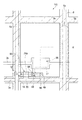
まず、第1の実施形態として、液晶装置について説明する。図1は、第1の実施形態にかかる液晶装置の等価回路図、図2は、液晶装置の平面図、図3は図2におけるA−A’線断面図である。
ここで、画素電極9a,9bの端部から離れた位置においても画素電極9a,9bからのフリンジ効果により液晶層102に電界が印加される。そして、間隙2の幅はフリンジ効果が間隙2内に届くよう、充分狭くしている。さらに、本発明による液晶装置は、液晶層102に電圧が印加されていないときは暗状態が表示され、液晶層102に電圧が印加されたときは明状態が表示される。したがって、画素電極9a,9bに電圧が印加されていないときにはその周囲の間隙2の液晶層102にも電圧が印加されないため、間隙を通過して反射層8によって反射された光は遮断される。そのため、間隙2には遮光層が設けられているとみなすことができる。一方、画素電極9a,9bに電圧が印加されているときには、そのフリンジ効果によって間隙2の液晶層にも電圧が印加されるために、反射光は遮断されない。従って、間隙2も画素と同様に有効な表示領域として機能する。たとえば、画素電極9aを備えた第1の画素と画素電極9bを備えた第2の画素の表示状態がいずれも暗状態ならば、隙間2も暗状態となる。そして、第1の画素と第2の画素の表示状態がいずれも明状態ならば、隙間2も明状態となる。
このように、暗状態を表示するときには、間隙2に反射層8が設けられているにもかかわらず、間隙に遮光膜が設けられている場合と同等な暗状態が得られる。一方、明状態を表示するときには、間隙2も画素電極9a,9bが備えられた領域と同様に、有効な表示領域として機能するため光の利用効率が高くなり、明るくなる。従って、コントラスト比が非常に高い表示が得られる。
間隙2の幅は、フリンジ効果が及ぶ距離のほぼ2倍以下が好ましい。2倍を越えると、画素電極9aからのフリンジ効果も画素電極9bからのフリンジ効果も及ばず、表示に利用できない領域が生じるため、好ましくない。そして、間隙2の最小幅は、加工上の制限で定まり、現状では0.3μm程度の値が下限である。これは、加工技術の進歩とともに変動する値となり、プロセス上安定に形成できるのは、後述する0.5μm程度の値となる。
画素電極9aからのフリンジ効果と、画素電極9bからのフリンジ効果が重なる領域では、両フリンジ効果の影響を受けて中間調の表示が行われる。この領域を表示に寄与させることで滑らかな画像を得ることが可能となる。
間隙2の幅がフリンジ効果が及ぶ距離のほぼ2倍の場合は、画素電極9aからのフリンジ効果と画素電極9bからのフリンジ効果のうち一方のみの効果の影響しか受けない領域が存在するが、その場合でも、フリンジ効果の影響を受けている領域を表示に寄与させることで滑らかな画像を得ることが可能となる。
以上、液晶装置120について説明したが、以下に示す変形例を用いることも好適である。上記した構造において、画素スイッチング用のTFT90は、LDD構造を有するものを用いているが、これはLDD構造を有する必要は無く、ドレイン側低濃度領域26、ソース側低濃度領域27の両方、あるいは片方を省略しても良い。この場合、TFT90の製造工程を短縮することが可能となる。
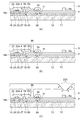
以下、図1〜図3で説明した液晶装置120の製造方法における一例を図面を用いて説明する。ここで、TFT90の製造方法等は公知であることから、詳細な説明は省略し、上記した実施形態の特徴を示す部分について詳細に説明する。なお、この構造を形成する手段としてはここで示した手段に限定されるものではなく、上記した構造を形成するための実施要件として説明を行うことを主たる目的としている。図4(a)〜(c)、図5(a),(b)は、本実施形態にかかる液晶装置120の製造工程を示す工程断面図である。
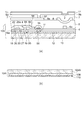
次に、上記実施形態の液晶装置を光変調手段として備えたプロジェクタ(投射型表示装置)の構成について、図6を参照して説明する。図6は本実施形態の反射型のプロジェクタの構成を示す図である。
Claims (8)
- 第1基板と、
光学的に透明な第2基板と、
前記第1基板と前記第2基板との間に設けられた液晶層と、
前記第1基板と前記液晶層との間に設けられた光反射性の複数の画素電極と、
前記画素電極を備えた画素と、
前記第2基板と前記液晶層との間に設けられた透光性を有する電極と、
前記画素電極よりも前記第1基板側間に、複数の前記画素電極のうち第1の画素電極と該第1の画素電極と隣り合う第2の画素電極との間の間隙の少なくとも一部に平面視したとき重なるように設けられた、該第1の画素電極と該第2の画素電極とが隣り合う方向の断面が前記液晶層と反対側に窪んだ凹面を有する反射層と、
を含むことを特徴とする液晶装置。 - 請求項1に記載の液晶装置であって、前記間隙における前記液晶層には、前記第1の画素電極の端縁からのフリンジ効果による電界と前記第2の画素電極の端縁からのフリンジ効果による電界が印加され、
当該電界により前記間隙が表示に利用されることを特徴とする液晶装置。 - 請求項1に記載の液晶装置であって、前記第1の画素電極を備えた第1の画素と前記第2の画素電極を備えた第2の画素の表示状態がともに明状態のときには、前記間隙も明状態であり、
前記第1の画素と前記第2の画素の表示状態がともに暗状態のときには、前記間隙も暗状態であることを特徴とする液晶装置。 - 請求項1乃至3のいずれか一項に記載の液晶装置であって、前記反射層の断面形状が放物線形状を有することを特徴とする液晶装置。
- 請求項1乃至4のいずれか一項に記載の液晶装置であって、前記反射層は、平面視したとき、前記画素電極の端縁の少なくとも一部と重なることを特徴とする液晶装置。
- 請求項1乃至5のいずれか一項に記載の液晶装置であって、前記第2基板側から前記間隙を通過した光は前記反射層によって反射され、さらに前記間隙内に収束されることを特徴とする液晶装置。
- 請求項1乃至6のいずれか一項に記載の液晶装置であって、前記反射層は、前記第1基板の一部を遮光する遮光層と同じ層を用いていることを特徴とする液晶装置。
- 請求項1乃至7のいずれか一項に記載の液晶装置を用いたことを特徴とするプロジェク
タ。
Priority Applications (3)
| Application Number | Priority Date | Filing Date | Title |
|---|---|---|---|
| JP2008221047A JP5256941B2 (ja) | 2008-08-29 | 2008-08-29 | 液晶装置およびプロジェクタ |
| US12/538,918 US8203663B2 (en) | 2008-08-29 | 2009-08-11 | Liquid crystal device and projector having particular concave reflective layer |
| CN200910163594.7A CN101661176B (zh) | 2008-08-29 | 2009-08-28 | 液晶装置及投影仪 |
Applications Claiming Priority (1)
| Application Number | Priority Date | Filing Date | Title |
|---|---|---|---|
| JP2008221047A JP5256941B2 (ja) | 2008-08-29 | 2008-08-29 | 液晶装置およびプロジェクタ |
Publications (2)
| Publication Number | Publication Date |
|---|---|
| JP2010054906A true JP2010054906A (ja) | 2010-03-11 |
| JP5256941B2 JP5256941B2 (ja) | 2013-08-07 |
Family
ID=41724891
Family Applications (1)
| Application Number | Title | Priority Date | Filing Date |
|---|---|---|---|
| JP2008221047A Expired - Fee Related JP5256941B2 (ja) | 2008-08-29 | 2008-08-29 | 液晶装置およびプロジェクタ |
Country Status (3)
| Country | Link |
|---|---|
| US (1) | US8203663B2 (ja) |
| JP (1) | JP5256941B2 (ja) |
| CN (1) | CN101661176B (ja) |
Cited By (1)
| Publication number | Priority date | Publication date | Assignee | Title |
|---|---|---|---|---|
| JP2013137476A (ja) * | 2011-12-28 | 2013-07-11 | Fujitsu Semiconductor Ltd | 半導体装置とその製造方法、及び反射型液晶表示装置 |
Families Citing this family (6)
| Publication number | Priority date | Publication date | Assignee | Title |
|---|---|---|---|---|
| CN102629048A (zh) | 2011-07-13 | 2012-08-08 | 京东方科技集团股份有限公司 | 液晶显示面板及其驱动方法 |
| US8710504B2 (en) * | 2011-12-18 | 2014-04-29 | Shenzhen China Star Optoelectronics Technology Co., Ltd. | Flat display panel and method for forming the same |
| CN102495504A (zh) * | 2011-12-19 | 2012-06-13 | 深圳市华星光电技术有限公司 | 平面显示面板及其形成方法 |
| JP5998626B2 (ja) * | 2012-05-15 | 2016-09-28 | セイコーエプソン株式会社 | 電気光学装置および電子機器 |
| KR102198029B1 (ko) * | 2012-06-15 | 2021-01-05 | 소니 주식회사 | 표시 장치, 반도체 장치 및 표시 장치의 제조 방법 |
| WO2024020767A1 (zh) * | 2022-07-26 | 2024-02-01 | 京东方科技集团股份有限公司 | 阵列基板及其制备方法、液晶盒、显示装置 |
Citations (5)
| Publication number | Priority date | Publication date | Assignee | Title |
|---|---|---|---|---|
| JPH08254715A (ja) * | 1994-05-13 | 1996-10-01 | Thomson Multimedia Sa | 液晶表示装置 |
| JPH10177169A (ja) * | 1996-10-18 | 1998-06-30 | Canon Inc | 反射型液晶装置用画素電極基板、該画素電極基板を用いた液晶装置及び該液晶装置を用いた表示装置 |
| JP2000010122A (ja) * | 1998-06-23 | 2000-01-14 | Seiko Epson Corp | 液晶パネル、それを用いた投射型液晶表示装置並びに電子機器、および液晶パネルの製造方法 |
| JP2002202501A (ja) * | 2000-12-27 | 2002-07-19 | Toshiba Corp | 反射型液晶表示装置 |
| JP2008134638A (ja) * | 2006-11-27 | 2008-06-12 | Samsung Electronics Co Ltd | 反射領域を持つ液晶表示装置 |
Family Cites Families (5)
| Publication number | Priority date | Publication date | Assignee | Title |
|---|---|---|---|---|
| JP3004534B2 (ja) | 1994-04-27 | 2000-01-31 | シャープ株式会社 | 液晶表示装置 |
| JP3249077B2 (ja) * | 1996-10-18 | 2002-01-21 | キヤノン株式会社 | マトリクス基板と液晶装置 |
| JP4123194B2 (ja) * | 2004-06-15 | 2008-07-23 | セイコーエプソン株式会社 | 液晶表示装置および電子機器 |
| JP2007133423A (ja) | 2007-01-09 | 2007-05-31 | Seiko Epson Corp | 液晶装置及び電子機器 |
| CN101295095B (zh) * | 2008-06-02 | 2010-07-28 | 友达光电股份有限公司 | 半穿透半反射式液晶显示面板及其制作方法 |
-
2008
- 2008-08-29 JP JP2008221047A patent/JP5256941B2/ja not_active Expired - Fee Related
-
2009
- 2009-08-11 US US12/538,918 patent/US8203663B2/en not_active Expired - Fee Related
- 2009-08-28 CN CN200910163594.7A patent/CN101661176B/zh not_active Expired - Fee Related
Patent Citations (5)
| Publication number | Priority date | Publication date | Assignee | Title |
|---|---|---|---|---|
| JPH08254715A (ja) * | 1994-05-13 | 1996-10-01 | Thomson Multimedia Sa | 液晶表示装置 |
| JPH10177169A (ja) * | 1996-10-18 | 1998-06-30 | Canon Inc | 反射型液晶装置用画素電極基板、該画素電極基板を用いた液晶装置及び該液晶装置を用いた表示装置 |
| JP2000010122A (ja) * | 1998-06-23 | 2000-01-14 | Seiko Epson Corp | 液晶パネル、それを用いた投射型液晶表示装置並びに電子機器、および液晶パネルの製造方法 |
| JP2002202501A (ja) * | 2000-12-27 | 2002-07-19 | Toshiba Corp | 反射型液晶表示装置 |
| JP2008134638A (ja) * | 2006-11-27 | 2008-06-12 | Samsung Electronics Co Ltd | 反射領域を持つ液晶表示装置 |
Cited By (1)
| Publication number | Priority date | Publication date | Assignee | Title |
|---|---|---|---|---|
| JP2013137476A (ja) * | 2011-12-28 | 2013-07-11 | Fujitsu Semiconductor Ltd | 半導体装置とその製造方法、及び反射型液晶表示装置 |
Also Published As
| Publication number | Publication date |
|---|---|
| CN101661176A (zh) | 2010-03-03 |
| US20100053482A1 (en) | 2010-03-04 |
| JP5256941B2 (ja) | 2013-08-07 |
| CN101661176B (zh) | 2014-04-09 |
| US8203663B2 (en) | 2012-06-19 |
Similar Documents
| Publication | Publication Date | Title |
|---|---|---|
| US6330112B1 (en) | Optical modulator and image projection display apparatus | |
| US8773615B2 (en) | Liquid crystal device and projector | |
| JP5256941B2 (ja) | 液晶装置およびプロジェクタ | |
| JPH10254370A (ja) | 表示パネル及びそれを用いた投射型表示装置 | |
| JP2007328129A (ja) | 液晶表示装置 | |
| US11422418B2 (en) | Liquid crystal device and electronic apparatus | |
| JP3873693B2 (ja) | 液晶装置及び投射型表示装置 | |
| US10656456B2 (en) | Electro-optical device and electronic apparatus | |
| KR101418838B1 (ko) | 액정 표시 장치 및 투사형 표시 장치 | |
| JP2007304607A (ja) | 投写型表示装置 | |
| JP6048075B2 (ja) | 液晶装置、及び電子機器 | |
| JP2012108458A (ja) | 投射型表示装置および光学ユニット | |
| US20020060780A1 (en) | Projector | |
| US10908444B2 (en) | Display device, method for producing display device, and display apparatus of projection type | |
| US11353729B2 (en) | Liquid crystal display device and projection type display device | |
| JP3649243B2 (ja) | 液晶装置および投射型表示装置 | |
| JP3777836B2 (ja) | 反射型光変調素子及び投写型表示装置 | |
| US11526057B2 (en) | Liquid crystal device comprising a wall portion extending along a third end and a fourth end of a pixel electrode and covered with the pixel electrode | |
| JP2005326608A (ja) | 液晶表示装置 | |
| JP4138354B2 (ja) | 液晶装置及びその製造方法、並びに投射型表示装置 | |
| JP7409236B2 (ja) | 電気光学装置、及び電子機器 | |
| JP3803530B2 (ja) | 液晶装置および該液晶装置を用いた投射型表示装置 | |
| JP2007171866A (ja) | 反射型液晶表示基板、反射型液晶表示装置、電子機器及び投射型表示装置 | |
| JP2025129552A (ja) | 電気光学装置および電子機器 | |
| JP2002214704A (ja) | プロジェクタ |
Legal Events
| Date | Code | Title | Description |
|---|---|---|---|
| A621 | Written request for application examination |
Free format text: JAPANESE INTERMEDIATE CODE: A621 Effective date: 20110808 |
|
| A131 | Notification of reasons for refusal |
Free format text: JAPANESE INTERMEDIATE CODE: A131 Effective date: 20121030 |
|
| A977 | Report on retrieval |
Free format text: JAPANESE INTERMEDIATE CODE: A971007 Effective date: 20121031 |
|
| A521 | Request for written amendment filed |
Free format text: JAPANESE INTERMEDIATE CODE: A523 Effective date: 20121213 |
|
| A131 | Notification of reasons for refusal |
Free format text: JAPANESE INTERMEDIATE CODE: A131 Effective date: 20130108 |
|
| A521 | Request for written amendment filed |
Free format text: JAPANESE INTERMEDIATE CODE: A523 Effective date: 20130307 |
|
| TRDD | Decision of grant or rejection written | ||
| A01 | Written decision to grant a patent or to grant a registration (utility model) |
Free format text: JAPANESE INTERMEDIATE CODE: A01 Effective date: 20130326 |
|
| A61 | First payment of annual fees (during grant procedure) |
Free format text: JAPANESE INTERMEDIATE CODE: A61 Effective date: 20130408 |
|
| FPAY | Renewal fee payment (event date is renewal date of database) |
Free format text: PAYMENT UNTIL: 20160502 Year of fee payment: 3 |
|
| R150 | Certificate of patent or registration of utility model |
Ref document number: 5256941 Country of ref document: JP Free format text: JAPANESE INTERMEDIATE CODE: R150 Free format text: JAPANESE INTERMEDIATE CODE: R150 |
|
| S531 | Written request for registration of change of domicile |
Free format text: JAPANESE INTERMEDIATE CODE: R313531 |
|
| R350 | Written notification of registration of transfer |
Free format text: JAPANESE INTERMEDIATE CODE: R350 |
|
| R250 | Receipt of annual fees |
Free format text: JAPANESE INTERMEDIATE CODE: R250 |
|
| R250 | Receipt of annual fees |
Free format text: JAPANESE INTERMEDIATE CODE: R250 |
|
| LAPS | Cancellation because of no payment of annual fees |