JP2012000954A - Device - Google Patents
Device Download PDFInfo
- Publication number
- JP2012000954A JP2012000954A JP2010140914A JP2010140914A JP2012000954A JP 2012000954 A JP2012000954 A JP 2012000954A JP 2010140914 A JP2010140914 A JP 2010140914A JP 2010140914 A JP2010140914 A JP 2010140914A JP 2012000954 A JP2012000954 A JP 2012000954A
- Authority
- JP
- Japan
- Prior art keywords
- information
- signal
- output
- selection
- input
- Prior art date
- Legal status (The legal status is an assumption and is not a legal conclusion. Google has not performed a legal analysis and makes no representation as to the accuracy of the status listed.)
- Pending
Links
Images


Classifications
-
- B—PERFORMING OPERATIONS; TRANSPORTING
- B41—PRINTING; LINING MACHINES; TYPEWRITERS; STAMPS
- B41J—TYPEWRITERS; SELECTIVE PRINTING MECHANISMS, i.e. MECHANISMS PRINTING OTHERWISE THAN FROM A FORME; CORRECTION OF TYPOGRAPHICAL ERRORS
- B41J2/00—Typewriters or selective printing mechanisms characterised by the printing or marking process for which they are designed
- B41J2/315—Typewriters or selective printing mechanisms characterised by the printing or marking process for which they are designed characterised by selective application of heat to a heat sensitive printing or impression-transfer material
- B41J2/32—Typewriters or selective printing mechanisms characterised by the printing or marking process for which they are designed characterised by selective application of heat to a heat sensitive printing or impression-transfer material using thermal heads
- B41J2/35—Typewriters or selective printing mechanisms characterised by the printing or marking process for which they are designed characterised by selective application of heat to a heat sensitive printing or impression-transfer material using thermal heads providing current or voltage to the thermal head
- B41J2/355—Control circuits for heating-element selection
-
- B—PERFORMING OPERATIONS; TRANSPORTING
- B41—PRINTING; LINING MACHINES; TYPEWRITERS; STAMPS
- B41J—TYPEWRITERS; SELECTIVE PRINTING MECHANISMS, i.e. MECHANISMS PRINTING OTHERWISE THAN FROM A FORME; CORRECTION OF TYPOGRAPHICAL ERRORS
- B41J2/00—Typewriters or selective printing mechanisms characterised by the printing or marking process for which they are designed
- B41J2/005—Typewriters or selective printing mechanisms characterised by the printing or marking process for which they are designed characterised by bringing liquid or particles selectively into contact with a printing material
- B41J2/01—Ink jet
- B41J2/07—Ink jet characterised by jet control
-
- B—PERFORMING OPERATIONS; TRANSPORTING
- B41—PRINTING; LINING MACHINES; TYPEWRITERS; STAMPS
- B41J—TYPEWRITERS; SELECTIVE PRINTING MECHANISMS, i.e. MECHANISMS PRINTING OTHERWISE THAN FROM A FORME; CORRECTION OF TYPOGRAPHICAL ERRORS
- B41J2/00—Typewriters or selective printing mechanisms characterised by the printing or marking process for which they are designed
- B41J2/005—Typewriters or selective printing mechanisms characterised by the printing or marking process for which they are designed characterised by bringing liquid or particles selectively into contact with a printing material
- B41J2/01—Ink jet
- B41J2/015—Ink jet characterised by the jet generation process
- B41J2/04—Ink jet characterised by the jet generation process generating single droplets or particles on demand
- B41J2/045—Ink jet characterised by the jet generation process generating single droplets or particles on demand by pressure, e.g. electromechanical transducers
- B41J2/04501—Control methods or devices therefor, e.g. driver circuits, control circuits
- B41J2/04541—Specific driving circuit
-
- B—PERFORMING OPERATIONS; TRANSPORTING
- B41—PRINTING; LINING MACHINES; TYPEWRITERS; STAMPS
- B41J—TYPEWRITERS; SELECTIVE PRINTING MECHANISMS, i.e. MECHANISMS PRINTING OTHERWISE THAN FROM A FORME; CORRECTION OF TYPOGRAPHICAL ERRORS
- B41J2/00—Typewriters or selective printing mechanisms characterised by the printing or marking process for which they are designed
- B41J2/005—Typewriters or selective printing mechanisms characterised by the printing or marking process for which they are designed characterised by bringing liquid or particles selectively into contact with a printing material
- B41J2/01—Ink jet
- B41J2/015—Ink jet characterised by the jet generation process
- B41J2/04—Ink jet characterised by the jet generation process generating single droplets or particles on demand
- B41J2/045—Ink jet characterised by the jet generation process generating single droplets or particles on demand by pressure, e.g. electromechanical transducers
- B41J2/04501—Control methods or devices therefor, e.g. driver circuits, control circuits
- B41J2/04546—Multiplexing
Landscapes
- Particle Formation And Scattering Control In Inkjet Printers (AREA)
Abstract
【課題】 デバイスと機器との接続する端子数を削減する。
【解決手段】 駆動素子と、前記駆動素子を制御する制御回路と、第1情報を生成する第1情報生成部と、第2情報を生成する第2情報生成部と、情報の出力端子と、外部から入力する選択情報に基づき、前記出力端子と前記第1、第2情報生成部との選択的な接続または前記出力端子をハイインピーダンス状態のいずれかを選択するスイッチとをそれぞれ有する第1素子基板及び第2素子基板を備えるデバイス。前記第1素子基板と第1信号線を介して接続され、第1選択情報を入力する第1の入力部と、前記第2素子基板と第2信号線を介して接続され、第2選択情報を入力する第2の入力部と、前記第1及び第2素子基板からそれぞれ出力される情報が共通の信号線を介して接続される出力部とを備える。
【選択図】 図2PROBLEM TO BE SOLVED: To reduce the number of terminals for connecting a device and a device.
A driving element, a control circuit that controls the driving element, a first information generating unit that generates first information, a second information generating unit that generates second information, an information output terminal, First elements each having a selective connection between the output terminal and the first and second information generating units or a switch for selecting either the high impedance state of the output terminal based on selection information input from the outside A device comprising a substrate and a second element substrate. A first input unit that is connected to the first element substrate via a first signal line and inputs first selection information; and a second input information that is connected to the second element substrate via a second signal line. And an output unit to which information output from each of the first and second element substrates is connected via a common signal line.
[Selection] Figure 2
Description
本発明は、素子基板を複数備えたデバイスに関し、特にデバイスの信号出力に関する。 The present invention relates to a device including a plurality of element substrates, and more particularly to signal output of the device.
特許文献1には、駆動素子として記録素子(ヒータ)を駆動する回路と複数の温度検知素子を同一半導体基板上に形成し、複数の温度検知素子を選択し、選択した温度検知素子の出力を共通の端子に出力する構成が開示されている。
In
しかしながら、素子基板を複数備えたデバイス(記録ヘッド)においては、各々の基板から出る温度検知素子の出力端子を個別に設ける構成にすると、記録ヘッドの端子数が増大する。このために、記録ヘッドと接続する機器(記録装置)の端子の数が増加し、記録装置の大型化やコストアップが生じる。また、温度検知素子の出力をそれぞれ個別の信号線を介して記録装置へ伝達すると、信号線のバラツキにより温度検知素子の出力値に差が生じてしまう。 However, in a device (recording head) provided with a plurality of element substrates, the number of terminals of the recording head increases if the output terminals of the temperature detection elements coming out of each substrate are individually provided. For this reason, the number of terminals of a device (recording apparatus) connected to the recording head increases, resulting in an increase in size and cost of the recording apparatus. Further, when the output of the temperature detection element is transmitted to the recording apparatus via the individual signal lines, a difference occurs in the output value of the temperature detection element due to variations in the signal lines.
上述した課題を解消するために、各々の基板から出る温度検知素子の出力端子を記録ヘッド内で共通に接続する構成を想定してみると、単純に共通接続した場合には、各基板からの出力電圧が共通接続した配線上で衝突する。このため正確な電圧値を記録ヘッドから出力することができない。このような課題は、記録装置に限らず他の機器にとっても共通する課題である。 In order to solve the above-mentioned problems, assuming a configuration in which the output terminals of the temperature detection elements coming out of the respective substrates are connected in common within the recording head, The output voltage collides on the commonly connected wiring. For this reason, an accurate voltage value cannot be output from the recording head. Such a problem is a problem common not only to the recording apparatus but also to other devices.
本発明は、上記課題を解決するデバイス及び、デバイスを接続する機器を提供することを目的とする。 An object of this invention is to provide the device which solves the said subject, and the apparatus which connects a device.
上記課題を解決するために、本発明のデバイスは、駆動素子と、前記駆動素子を制御する制御回路と、第1情報を生成する第1情報生成部と、第2情報を生成する第2情報生成部と、情報の出力端子と、外部から入力する選択情報に基づき、前記出力端子と前記第1、第2情報生成部との選択的な接続または前記出力端子をハイインピーダンス状態のいずれかを選択するスイッチとをそれぞれ有する第1素子基板及び第2素子基板を備えるデバイスであって、
前記第1素子基板と第1信号線を介して接続され、第1選択情報を入力する第1の入力部と、前記第2素子基板と第2信号線を介して接続され、第2選択情報を入力する第2の入力部と、前記第1及び第2素子基板からそれぞれ出力される情報が共通の信号線を介して接続される出力部とを備えることを特徴とする。
In order to solve the above-described problems, a device of the present invention includes a drive element, a control circuit that controls the drive element, a first information generation unit that generates first information, and second information that generates second information. Based on selection information input from the generation unit, the information output terminal, and the outside, either the selective connection between the output terminal and the first or second information generation unit or the output terminal in a high impedance state. A device comprising a first element substrate and a second element substrate each having a switch to be selected,
A first input unit that is connected to the first element substrate via a first signal line and inputs first selection information; and a second input information that is connected to the second element substrate via a second signal line. And a second input unit for inputting information, and an output unit to which information output from each of the first and second element substrates is connected through a common signal line.
本発明に寄れば、記録ヘッド等のデバイスが接続する機器(装置)へ出力する信号の端子数の増加を抑制しつつ、複数の素子基板から信号や情報を取得することができる。 According to the present invention, signals and information can be acquired from a plurality of element substrates while suppressing an increase in the number of terminals of signals output to a device (apparatus) connected to a device such as a recording head.
(第1の実施例)
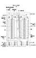
図1は、第1の実施例における素子基板101の構成を説明する図である。ヒータ102はインクを吐出する記録素子である。この実施例では、駆動素子として記録素子を備えた素子基板について説明する。複数の記録素子102が配列され、a列(インク供給口の両側に2列)とb列(インク供給口の両側に2列)が配置されている。
(First embodiment)
FIG. 1 is a diagram illustrating the configuration of the element substrate 101 in the first embodiment. The
シフトレジスタ(S/R)106は、Mビットの記録データを一時的に格納する。ラッチ回路105は、シフトレジスタ(S/R)106に格納された記録データを一括して保持する。ブロック選択回路(デコーダ)104はヒータおよびスイッチング素子が形成するN個のブロックから所望のブロックを選択するである。これら上述したシフトレジスタ106、ラッチ105、デコーダ104は、記録素子の駆動を制御する制御回路である。
The shift register (S / R) 106 temporarily stores M-bit recording data. The
素子基板を制御する機器(例えばプリンタ本体)から供給されるクロック信号CLKが端子109に入力される。このクロック信号に、同期してシリアル転送されるMビットの記録データ信号DATAが端子110−aおよび110−bから入力され、シフトレジスタ106に順次格納される。その後ラッチ信号端子108から入力されるラッチ信号LTに従ってこのシリアルデータがラッチ回路105に保持される。このときブロック選択回路104に入力される信号も記録データ信号に続いてシリアル転送され、デコーダによりN本のブロック選択信号に変換されてグループ1〜Mへ接続される。
A clock signal CLK supplied from a device (for example, a printer main body) that controls the element substrate is input to the
インク供給口210は、基板の裏面からインクを供給する。この場合は同一基板内に2つの供給口を設けてある。温度検知素子150は、素子基板内に3箇所に設けられている。温度検知素子150は、例えばp−n接合ダイオードの電圧−電流特性の温度特性を利用したものが用いられる。抵抗モニター素子151は記録素子となるヒータの抵抗値をモニターするためのであり、基板内に作りこまれたヒータの抵抗値に対応する抵抗値をもつ。これらの温度検知素子150、抵抗モニター素子151は素子基板に設けられた情報生成部(信号生成部)である。温度検知素子150は、温度情報を生成する温度情報生成部である。
The
切換回路161は、温度検知素子150や抵抗モニター素子151の出力が接続され、これらを切換えてアナログ出力端子163(A_OUT)から出力する。選択回路164は、切換回路161の出力を選択する。入力端子162は、外部からアナログ出力選択信号(SEL)を入力し、この信号を選択回路164へ供給する。また、切換回路161にはロジック電源電圧VDD130およびVHT電圧132が接続されている。この構成により、温度検知素子、抵抗モニター素子、ロジック電源電圧VDDおよびVHT電圧がそれぞれ所望のタイミングでアナログ出力端子163から出力される。
The switching circuit 161 is connected to the outputs of the
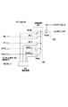
図2は、切換回路161を説明する図である。切換回路161は複数のアナログSW321を備えている。アナログSW321は、それぞれ一方の端子に、温度検知素子150、抵抗モニター素子151、ロジック電源電圧VDDを分圧する分圧抵抗、VHT電圧を分圧する分圧抵抗に接続されている。これらの抵抗回路は、別の表現をすれば電圧情報を生成する回路である。
FIG. 2 is a diagram for explaining the switching circuit 161. The switching circuit 161 includes a plurality of
アナログSW321の1つは、ハイインピーダンス(HZ)状態になるオープンチャネル(Open ch)の状態となっている。これら各アナログSW321の他方の端子を共通接続して、アナログ出力端子163(A_OUT)に接続する。
One of the
選択回路164は、それぞれのアナログSWに対応したアナログSW選択信号(選択情報)322を出力し、この信号によりアナログSWが1つ選択される。これにより、アナログSW選択信号322を制御することで、切換回路161から選択的に信号が出力される。図2のアナログSWの1つは、オープンチャネル(Open ch)の状態であるので、そのアナログSWを選択すればアナログ出力端子163をHZ状態(ハイインピーダンス状態)にできる。
The
なお、ロジック電源電圧VDDおよびVHT電圧は、それぞれ分圧抵抗311の一方の端子に接続され、他方の端子はスイッチングトランジスタ312に接続されている。スイッチングトランジスタ312のゲートにはそれぞれVDD電圧およびVHT電圧を選択するアナログSW選択信号が入力されている。これにより選択されたときにだけ分圧抵抗に電流が流れ、選択されなければ分圧抵抗に電流が流れないようにしている。
The logic power supply voltage VDD and the VHT voltage are each connected to one terminal of the voltage dividing resistor 311, and the other terminal is connected to the switching
ロジック電源電圧VDDおよびVHT電圧は、それぞれ分圧抵抗311により温度検知素子150の出力電圧と略同レベルの電圧に調整されている。例えば、温度検知素子としてp−n接合ダイオードを用いた場合には、その出力電圧は室温においてはほぼ0.6ボルトから0.7ボルトである。VDD電圧が3.3ボルト、VHT電圧が24ボルトであれば、それらの電圧を0.6ボルトから0.7ボルトに成るように、分圧抵抗の値を定める。
The logic power supply voltage VDD and the VHT voltage are respectively adjusted to voltages substantially equal to the output voltage of the
図3は、記録素子駆動回路205の説明図である。この記録素子駆動回路205は、ヒータ選択回路115、電圧変換回路107、スイッチング素子103、からなるである。ヒータ選択回路115は、任意のヒータを選択するための回路であり、電圧変換回路107はヒータ選択回路115の出力信号の電圧レベルをスイッチング素子を駆動する電圧レベルに変換する。ここでヒータ102、スイッチング素子103、ヒータ選択回路115は、N個づつで1つのグループを形成する。このグループをM(複数)個備えて記録素子列を構成している。なお、このN個の記録素子は、ブロック選択信号118の信号に従い、時分割で1つ選択され駆動するいわゆる時分割駆動を行う。
FIG. 3 is an explanatory diagram of the recording
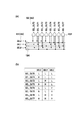
図4(a)は、選択回路164の構成を説明する図である。ここではアナログSW選択信号322が8本の場合の回路構成を示す。SEL信号162は3ビット(SEL0からSEL2)で構成されている。選択回路164は、インバータ1001およびNAND回路1002で構成されることで、アナログSW選択信号322となるSEL_OUT0からSEL_OUT7の8本の信号を生成することができる。図4(b)は、選択回路の真理値表であり、各入力端子SEL0からSEL2の論理状態を定めることで、SEL_OUT0から7の出力が一義的に出力できる。例えば、SEL0〜SEL2がすべてLであれば、SEL_OUT0が有効になる。
FIG. 4A is a diagram illustrating the configuration of the
図5は、電圧変換回路107の構成を説明する図である。この構成により信号の電圧振幅を、ヒータ選択回路の出力の電圧振幅(第1電源電圧)よりも高い電圧(第2電源電圧)に変換される。変換された信号は、スイッチング素子であるMOSトランジスタ103のゲートに印加され、MOSトランジスタ103に接続されたヒータ102に電流がながれ、駆動される。ここでより高い第2電圧に変換を行なうのは、ヒータ駆動MOSトランジスタ103のゲートに印加する電圧を高くすることで、そのオン抵抗を低下させ、高い効率でヒータに電流を流すことを可能とするためである。この第2電源電圧の電圧値は、回路のブレイクダウン耐圧及びMOSのゲート耐圧を越えることなく、可能な限り高く設定することが望ましい。なお、図1に示す駆動電圧発生回路131(VHTバッファ)は、VHT電圧132から所望の第2電源電圧を生成する。
FIG. 5 is a diagram for explaining the configuration of the
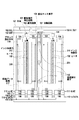
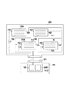
図6は、第1の実施例における記録ヘッドを説明する図である。記録ヘッド900は、4つの記録素子基板101A〜101Dを備えたデバイスである。記録素子基板はそれぞれ、図1に示したように、4つのヒータ列を備えている。接続部901は、機器(記録装置の本体)と接続する。接続部901は、4つの素子基板の入力端子162とそれぞれ接続する入力部と、4つの素子基板の出力端子163と共通に接続する出力部とを備えている。説明を簡単にするために、必要最低限の信号線を記載している。図1や図4で説明したように、各記録素子基板には、入力端子162に3ビットの選択信号(SEL0〜SEL2)が入力される。この選択信号は、接続部901から個別に供給される。一方、選択信号に従って、アナログ出力端子163からアナログ信号が出力する。このアナログ出力端子163は、各記録素子基板のアナログ出力端子163と接続されている。
FIG. 6 is a diagram for explaining the recording head in the first embodiment. The
この記録ヘッド900と接続する記録装置1000は、接続部1001を備えている。制御部1002は、記録装置1000の制御を行う。制御部1002は、記録ヘッドへ出力する選択信号を生成する信号生成部1003と、記録ヘッドから入力するアナログ信号を処理する処理回路1004Aを備えている。制御部1002は、CPUやメモリ、ASIC(特定用途集積回路)などで構成されている。
A
信号生成部1003は、例えば、記録素子基板101Aの温度検知素子150の情報を取得するために選択信号(SEL0〜SEL2)を出力する。この場合、信号生成部1003は、記録素子基板101B、記録素子基板101C、記録素子基板101Dに対して、オープンチャネルを選択する信号を出力する。このように、選択信号を出力すれば、記録素子基板101B、101C、101Dの出力端子はハイインピーダンス状態になるので、記録素子基板101Aの温度検知素子の情報を取得できる。同様に、記録素子基板101Bの温度検知素子150の情報を取得する場合には、他の記録素子基板101A、101C、101Dに対して、オープンチャネルを選択する信号を出力する。
For example, the
以上のように、信号生成部1003は、4つの素子基板のうち1つを選択するように、選択信号を生成する。これにより、アナログ出力端子163が共通に接続した状態であっても、記録装置は、適切に信号を受信できる。なお、信号生成部1003は、記録装置の動作内容により、4つの素子基板を選択する制御を行う。
As described above, the
以上の構成により、デバイス(記録ヘッド)が、機器(記録装置)へ出力する信号の端子数の増加を抑制しつつ、複数の素子基板からアナログ形式の信号や情報を取得することができる。 With the above configuration, the device (recording head) can acquire analog signals and information from a plurality of element substrates while suppressing an increase in the number of terminals of signals output to the device (recording apparatus).
(第2の実施例)
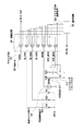
図7は、第2の実施例における素子基板の構成を説明する図である。図1と同様の番号の部分については説明を省略する。相違する点について説明する。図7において、ヒート信号生成回路411は、ヒータを駆動するスイッチング素子に供給するヒート(HE)信号413を生成する。ヒート信号生成回路411は、ヒートパルス幅信号(パルス幅情報)412に基づいてヒート信号413を生成する。ヒートパルス幅信号(パルス幅情報)412は、データ信号110と同じ端子を介して、シフトレジスタ106へシリアル転送される。ヒート信号生成回路411で生成されたヒート信号413は、図9に示す記録素子駆動回路205において、ヒータ選択回路115は、記録データ信号107、ブロック選択信号118、ヒート信号413とを論理積を行ない、その結果を電圧変換回路107出力する。
(Second embodiment)
FIG. 7 is a diagram illustrating the configuration of the element substrate in the second embodiment. The description of the same reference numerals as in FIG. 1 is omitted. Differences will be described. In FIG. 7, the heat
切換回路461は各ヒータ列205に対応したヒート信号413を入力し、これらを切換えてデジタル出力端子463(D_OUT)から出力する。また、切換回路461は、2つのシフトレジスタ106へそれぞれ入力された記録データ信号も入力する。選択回路464は切換回路461の出力を選択する。入力端子462は選択回路464に入力するデジタル出力選択信号(SEL)を入力する。従って、ヒート信号や記録データ信号のいずれかを選択して、出力することで信号の内容の確認をすることができる。
The
図8は、切換回路461を説明する図である。切換回路461は、3ステートバッファ521を複数備えている。3ステートバッファ521は、Hi、Lo、HZの3つの状態を出力する。各ステートバッファには、それぞれ4つのヒート信号(HE_1〜HE_4)、2つの記録データ信号(DATA_1、DATA_2)が接続されている。一方で、出力端子は共通に接続されている。この共通接続された出力は、さらに3ステートバッファ522に入力する。この3ステートバッファ522の出力が、デジタル出力端子463に接続される。
FIG. 8 is a diagram for explaining the
選択回路464は、第1の実施例と同様に、各3ステートバッファ521に対応したデジタル信号選択信号422を出力し、これによりそれぞれの3ステートバッファの状態が一義的に選択される。そして、選択された3ステートバッファ以外はHZ状態(ハイインピーダンス状態)になるように信号422は出力される。したがって、4つのヒート信号(HE_1〜HE_4)、2つの記録データ信号(DATA_1、DATA_2)のうちのいずれが選択された場合には、3ステートバッファ522、デジタル出力端子463を介して、選択された信号が、出力される。
As in the first embodiment, the
一方、4つのヒート信号(HE_1〜HE_4)、2つの記録データ信号(DATA_1、DATA_2)のいずれも選択されない場合には、3ステートバッファ522をHZ(ハイインピーダンス)にする。これにより、デジタル出力端子463はHZ状態(ハイインピーダンス状態)となる。デジタル出力端子463から信号は出力されない。この実施例では、オープンチャネル(Open ch)431に対応した3ステートバッファ521の入力はGNDに接続している。
On the other hand, when none of the four heat signals (HE_1 to HE_4) and the two recording data signals (DATA_1, DATA_2) are selected, the 3-
なお、図10は、3ステートバッファ522の実施例を説明する図である。入力端子811は信号を入力する。State端子812に入力される信号を入力する。813、814は出力段のnMOSトランジスタである。この構成により、仮に誤って信号が入力した場合にも、基板内部の寄生トランジスタが動作するなどして異常電流が流れることを防止できる。
FIG. 10 is a diagram for explaining an embodiment of the three-
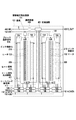
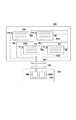
図11は、第2の実施例における記録ヘッドを説明する図である。第1の実施例と同じ点については説明を省き、相違する点について説明する。第2の実施例では、入力端子462に3ビットの選択信号(SEL0〜SEL2)が入力される。この選択信号に従って、デジタル出力端子463からデジタル信号が出力する。記録装置1000の構成も、第1の実施例のアナログ信号を処理する処理回路1004Aの代わりに、デジタル信号を処理する処理回路1004Dを備えている。信号生成部1003の制御についても、第1の実施例と同様であるので説明は省く。
FIG. 11 is a diagram for explaining a recording head in the second embodiment. The description of the same points as in the first embodiment will be omitted, and the differences will be described. In the second embodiment, a 3-bit selection signal (SEL0 to SEL2) is input to the
以上の構成により、デバイス(記録ヘッド)がデバイス(記録装置)へ出力する信号の端子数の増加を抑制しつつ、複数の素子基板からデジタル形式の信号や情報を取得することができる。 With the above configuration, it is possible to acquire digital signals and information from a plurality of element substrates while suppressing an increase in the number of terminals of signals output from the device (recording head) to the device (recording apparatus).
(第3の実施例)
図12は、第3の実施例における素子基板の構成を説明する図である。図1と同様の番号の部分については説明を省略する。図1では入力端子162から3ビットの信号(SEL0〜SEL2)を入力する形態であったが、図12では、シリアル転送されるMビットの記録データ信号DATAとともに選択信号を入力する。つまり、選択信号(SEL0〜SEL2)は、記録装置から端子110−aを介して入力する。この選択信号は、シフトレジスタ(S/R)106に入力し、ラッチ回路105で保持され、選択回路164へ転送される。
(Third embodiment)
FIG. 12 is a diagram illustrating the configuration of the element substrate in the third embodiment. The description of the same reference numerals as in FIG. 1 is omitted. In FIG. 1, a 3-bit signal (SEL0 to SEL2) is input from the
図14は、第3の実施例における記録ヘッドを説明する図である。第1の実施例と同じ点については説明を省き、相違する点について説明する。第3の実施例では、端子110−aに、シリアル形式で3ビットの選択信号(SEL0〜SEL2)が入力される。この選択信号に従って、アナログ出力端子163からアナログ信号が出力する。記録装置1000の構成は、第1の実施例と同様に、アナログ信号を処理する処理回路1004Aを備えている。また、記録装置1000は、信号生成部1005は、第1の実施例や第2の実施例と異なり、シリアルデータを生成する。信号生成部1005は、例えば、記録データ信号DATAの前に選択信号の情報を転送する。
FIG. 14 is a diagram for explaining a recording head in the third embodiment. The description of the same points as in the first embodiment will be omitted, and the differences will be described. In the third embodiment, a 3-bit selection signal (SEL0 to SEL2) is input to the terminal 110-a in a serial format. According to this selection signal, an analog signal is output from the
以上の構成により、選択信号の入力端子を他の信号の入力端子と共用することで、記録ヘッドが記録装置から入力する信号の端子数の増加を抑制しつつ、複数の素子基板からアナログ形式の信号や情報を取得することができる。 With the above configuration, by sharing the input terminal of the selection signal with the input terminal of another signal, an increase in the number of terminals of the signal input from the recording apparatus to the recording head is suppressed, and an analog format is generated from a plurality of element substrates. Signals and information can be acquired.
(第4の実施例)
図13は、第4の実施例における素子基板の構成を説明する図である。図1や図12と同様の番号の部分については説明を省略する。図12では、記録ヘッドからアナログ信号を出力する形態であったが、図13は、記録ヘッドからデジタル信号を出力する形態である。第3の実施例と同様に、端子110−aに、シリアル形式で3ビットの選択信号(SEL0〜SEL2)が入力される。なお、第4の実施例における記録ヘッドを説明は省く。
(Fourth embodiment)
FIG. 13 is a diagram for explaining the configuration of the element substrate in the fourth embodiment. The description of the same reference numerals as those in FIGS. 1 and 12 is omitted. In FIG. 12, the analog signal is output from the recording head, but FIG. 13 is the output of the digital signal from the recording head. As in the third embodiment, a 3-bit selection signal (SEL0 to SEL2) is input to the terminal 110-a in a serial format. The description of the recording head in the fourth embodiment is omitted.
以上の構成により、選択信号の入力端子を他の信号の入力端子と共用することで、記録ヘッドが記録装置から入力する信号の端子数の増加を抑制しつつ、複数の素子基板からデジタル形式の信号や情報を取得することができる。 With the above configuration, by sharing the input terminal of the selection signal with the input terminal of other signals, the increase in the number of terminals of the signal input from the recording apparatus to the recording head is suppressed, and the digital format is obtained from a plurality of element substrates. Signals and information can be acquired.
(その他の実施形態)
以上、デバイスを例として記録ヘッドについて説明したが、他のデバイスでも同様の構成をとることができる。例えば、光学センサを備えた読取ユニットを制御する読取装置にも適用できる。
(Other embodiments)
The recording head has been described above using the device as an example, but other devices can have the same configuration. For example, the present invention can be applied to a reading apparatus that controls a reading unit including an optical sensor.
161 切替回路
164 選択回路
161
Claims (3)
前記第1素子基板と第1信号線を介して接続され、第1選択情報を入力する第1入力部と、
前記第2素子基板と第2信号線を介して接続され、第2選択情報を入力する第2入力部と、
前記第1及び第2素子基板からそれぞれ出力される情報が共通の信号線を介して接続される出力部とを備えることを特徴とするデバイス。 A drive element, a control circuit that controls the drive element, a first information generation unit that generates first information, a second information generation unit that generates second information, an information output terminal, and an external input A first element substrate and a second element substrate each having a selective connection between the output terminal and the first and second information generation units or a switch for selecting either the high impedance state of the output terminal based on selection information; A device comprising an element substrate,
A first input unit connected to the first element substrate via a first signal line and inputting first selection information;
A second input unit that is connected to the second element substrate via a second signal line and inputs second selection information;
And an output unit to which information output from each of the first and second element substrates is connected via a common signal line.
Priority Applications (4)
| Application Number | Priority Date | Filing Date | Title |
|---|---|---|---|
| JP2010140914A JP2012000954A (en) | 2010-06-21 | 2010-06-21 | Device |
| US12/964,676 US8400484B2 (en) | 2010-06-21 | 2010-12-09 | Device and apparatus for controlling same |
| US13/767,138 US8508565B2 (en) | 2010-06-21 | 2013-02-14 | Device and apparatus for controlling same |
| US13/940,632 US9096058B2 (en) | 2010-06-21 | 2013-07-12 | Device and apparatus for controlling same |
Applications Claiming Priority (1)
| Application Number | Priority Date | Filing Date | Title |
|---|---|---|---|
| JP2010140914A JP2012000954A (en) | 2010-06-21 | 2010-06-21 | Device |
Publications (2)
| Publication Number | Publication Date |
|---|---|
| JP2012000954A true JP2012000954A (en) | 2012-01-05 |
| JP2012000954A5 JP2012000954A5 (en) | 2013-08-08 |
Family
ID=45328289
Family Applications (1)
| Application Number | Title | Priority Date | Filing Date |
|---|---|---|---|
| JP2010140914A Pending JP2012000954A (en) | 2010-06-21 | 2010-06-21 | Device |
Country Status (2)
| Country | Link |
|---|---|
| US (3) | US8400484B2 (en) |
| JP (1) | JP2012000954A (en) |
Cited By (4)
| Publication number | Priority date | Publication date | Assignee | Title |
|---|---|---|---|---|
| JP2017530890A (en) * | 2014-10-28 | 2017-10-19 | ヒューレット−パッカード デベロップメント カンパニー エル.ピー.Hewlett‐Packard Development Company, L.P. | Wide array printhead module |
| JP2018111306A (en) * | 2017-01-06 | 2018-07-19 | キヤノン株式会社 | Recording head and recording apparatus |
| JP2019006108A (en) * | 2017-06-28 | 2019-01-17 | キヤノン株式会社 | Recording apparatus and recording head substrate |
| US10406808B2 (en) | 2017-06-28 | 2019-09-10 | Canon Kabushiki Kaisha | Printing apparatus and printhead substrate |
Families Citing this family (3)
| Publication number | Priority date | Publication date | Assignee | Title |
|---|---|---|---|---|
| JP2012000954A (en) * | 2010-06-21 | 2012-01-05 | Canon Inc | Device |
| JP7204425B2 (en) * | 2018-11-01 | 2023-01-16 | キヤノン株式会社 | DEVICE SUBSTRATE, PRINT HEAD, AND PRINTING DEVICE |
| EP3710267B1 (en) * | 2019-02-06 | 2024-03-27 | Hewlett-Packard Development Company, L.P. | Temperature detection and control |
Citations (7)
| Publication number | Priority date | Publication date | Assignee | Title |
|---|---|---|---|---|
| JPH064825U (en) * | 1992-06-26 | 1994-01-21 | グラフテック株式会社 | Cordless digitizer |
| JPH1016230A (en) * | 1996-07-04 | 1998-01-20 | Canon Inc | Printheads and printing equipment |
| JPH1134380A (en) * | 1997-07-15 | 1999-02-09 | Ricoh Co Ltd | Thermal head drive |
| JP2001156702A (en) * | 1999-11-24 | 2001-06-08 | Sharp Corp | Mobile communication device |
| JP2001232774A (en) * | 2000-02-18 | 2001-08-28 | Seiko Epson Corp | Inkjet head drive circuit |
| JP2008260129A (en) * | 2007-04-10 | 2008-10-30 | Sony Corp | Liquid ejection device and control method of liquid ejection device |
| JP2009101576A (en) * | 2007-10-23 | 2009-05-14 | Canon Inc | Inkjet recording head |
Family Cites Families (5)
| Publication number | Priority date | Publication date | Assignee | Title |
|---|---|---|---|---|
| US7101099B1 (en) * | 1998-08-19 | 2006-09-05 | Canon Kabushiki Kaisha | Printing head, head cartridge having printing head, printing apparatus using printing head, and printing head substrate |
| JP2003226012A (en) | 2002-02-01 | 2003-08-12 | Canon Inc | Inkjet printer head |
| JP2005169867A (en) * | 2003-12-11 | 2005-06-30 | Canon Inc | Recording head element substrate, recording head, and recording apparatus |
| JP4785375B2 (en) * | 2004-12-09 | 2011-10-05 | キヤノン株式会社 | Inkjet recording head substrate, recording head, head cartridge, and recording apparatus |
| JP2012000954A (en) * | 2010-06-21 | 2012-01-05 | Canon Inc | Device |
-
2010
- 2010-06-21 JP JP2010140914A patent/JP2012000954A/en active Pending
- 2010-12-09 US US12/964,676 patent/US8400484B2/en not_active Expired - Fee Related
-
2013
- 2013-02-14 US US13/767,138 patent/US8508565B2/en not_active Expired - Fee Related
- 2013-07-12 US US13/940,632 patent/US9096058B2/en active Active
Patent Citations (7)
| Publication number | Priority date | Publication date | Assignee | Title |
|---|---|---|---|---|
| JPH064825U (en) * | 1992-06-26 | 1994-01-21 | グラフテック株式会社 | Cordless digitizer |
| JPH1016230A (en) * | 1996-07-04 | 1998-01-20 | Canon Inc | Printheads and printing equipment |
| JPH1134380A (en) * | 1997-07-15 | 1999-02-09 | Ricoh Co Ltd | Thermal head drive |
| JP2001156702A (en) * | 1999-11-24 | 2001-06-08 | Sharp Corp | Mobile communication device |
| JP2001232774A (en) * | 2000-02-18 | 2001-08-28 | Seiko Epson Corp | Inkjet head drive circuit |
| JP2008260129A (en) * | 2007-04-10 | 2008-10-30 | Sony Corp | Liquid ejection device and control method of liquid ejection device |
| JP2009101576A (en) * | 2007-10-23 | 2009-05-14 | Canon Inc | Inkjet recording head |
Cited By (7)
| Publication number | Priority date | Publication date | Assignee | Title |
|---|---|---|---|---|
| JP2017530890A (en) * | 2014-10-28 | 2017-10-19 | ヒューレット−パッカード デベロップメント カンパニー エル.ピー.Hewlett‐Packard Development Company, L.P. | Wide array printhead module |
| JP2018111306A (en) * | 2017-01-06 | 2018-07-19 | キヤノン株式会社 | Recording head and recording apparatus |
| JP7045845B2 (en) | 2017-01-06 | 2022-04-01 | キヤノン株式会社 | Recording head and recording device |
| JP2019006108A (en) * | 2017-06-28 | 2019-01-17 | キヤノン株式会社 | Recording apparatus and recording head substrate |
| US10406808B2 (en) | 2017-06-28 | 2019-09-10 | Canon Kabushiki Kaisha | Printing apparatus and printhead substrate |
| US10987922B2 (en) | 2017-06-28 | 2021-04-27 | Canon Kabushiki Kaisha | Printing apparatus and printhead substrate |
| JP7090474B2 (en) | 2017-06-28 | 2022-06-24 | キヤノン株式会社 | Recording device and recording head board |
Also Published As
| Publication number | Publication date |
|---|---|
| US20130155165A1 (en) | 2013-06-20 |
| US9096058B2 (en) | 2015-08-04 |
| US8400484B2 (en) | 2013-03-19 |
| US8508565B2 (en) | 2013-08-13 |
| US20110310210A1 (en) | 2011-12-22 |
| US20130300789A1 (en) | 2013-11-14 |
Similar Documents
| Publication | Publication Date | Title |
|---|---|---|
| US9096058B2 (en) | Device and apparatus for controlling same | |
| US8740350B2 (en) | Inkjet recording head substrate and drive control method, inkjet recording head, inkjet recording head cartridge and inkjet recording apparatus | |
| JP2003218687A5 (en) | ||
| US5933161A (en) | Ink-jet recorder having a driving circuit for driving heat-generating elements | |
| KR101598077B1 (en) | A source driver and display apparatus including the same | |
| JP2004312472A (en) | Solid-state imaging device and imaging method | |
| JP5665364B2 (en) | Recording element substrate | |
| US20110148842A1 (en) | Source driver for liquid crystal display panel | |
| JP5063314B2 (en) | Element substrate, recording head, head cartridge, and recording apparatus | |
| JP2792511B2 (en) | Display driver | |
| JP5254525B2 (en) | Display device drive circuit | |
| US6359639B1 (en) | Thermal head driving integrated circuit | |
| JP5094745B2 (en) | Thermal head and image forming apparatus using the same | |
| JP5031455B2 (en) | Element substrate for recording head, recording head, and recording apparatus using the recording head | |
| JP4116003B2 (en) | Current drive circuit | |
| CN104875495B (en) | Printing apparatus and printhead | |
| WO2010053938A1 (en) | Non-binary decoder architecture and control signal logic for reduced circuit complexity | |
| TWI398848B (en) | Source driving circuit | |
| KR20060064653A (en) | Semiconductor integrated circuit device | |
| US7382365B2 (en) | Semiconductor device and driver | |
| US7806501B2 (en) | Driving apparatus, LED head and image forming apparatus | |
| JP4915914B2 (en) | Integrated circuit for driving thermal head | |
| JP2005199460A (en) | Image recording head and image recording apparatus | |
| JP2007203665A (en) | Inkjet recording head | |
| JPH0550636A (en) | Thermal head |
Legal Events
| Date | Code | Title | Description |
|---|---|---|---|
| A521 | Request for written amendment filed |
Free format text: JAPANESE INTERMEDIATE CODE: A523 Effective date: 20130621 |
|
| A621 | Written request for application examination |
Free format text: JAPANESE INTERMEDIATE CODE: A621 Effective date: 20130621 |
|
| A977 | Report on retrieval |
Free format text: JAPANESE INTERMEDIATE CODE: A971007 Effective date: 20140122 |
|
| A131 | Notification of reasons for refusal |
Free format text: JAPANESE INTERMEDIATE CODE: A131 Effective date: 20140204 |
|
| A521 | Request for written amendment filed |
Free format text: JAPANESE INTERMEDIATE CODE: A523 Effective date: 20140407 |
|
| A02 | Decision of refusal |
Free format text: JAPANESE INTERMEDIATE CODE: A02 Effective date: 20150203 |