JP2012124643A - Receiving device and data transfer device - Google Patents
Receiving device and data transfer device Download PDFInfo
- Publication number
- JP2012124643A JP2012124643A JP2010272421A JP2010272421A JP2012124643A JP 2012124643 A JP2012124643 A JP 2012124643A JP 2010272421 A JP2010272421 A JP 2010272421A JP 2010272421 A JP2010272421 A JP 2010272421A JP 2012124643 A JP2012124643 A JP 2012124643A
- Authority
- JP
- Japan
- Prior art keywords
- data
- unit
- error detection
- bits
- conversion
- Prior art date
- Legal status (The legal status is an assumption and is not a legal conclusion. Google has not performed a legal analysis and makes no representation as to the accuracy of the status listed.)
- Pending
Links
- 238000012546 transfer Methods 0.000 title claims abstract description 41
- 238000006243 chemical reaction Methods 0.000 claims abstract description 91
- 238000001514 detection method Methods 0.000 claims abstract description 39
- 238000000034 method Methods 0.000 claims abstract description 13
- 239000000284 extract Substances 0.000 claims abstract description 4
- 238000012545 processing Methods 0.000 abstract description 6
- 238000004904 shortening Methods 0.000 abstract 1
- 230000005540 biological transmission Effects 0.000 description 25
- 238000012937 correction Methods 0.000 description 10
- 238000004891 communication Methods 0.000 description 9
- 230000009466 transformation Effects 0.000 description 9
- 238000010586 diagram Methods 0.000 description 5
- 238000000605 extraction Methods 0.000 description 2
- 230000001131 transforming effect Effects 0.000 description 2
- 239000002131 composite material Substances 0.000 description 1
- 125000004122 cyclic group Chemical group 0.000 description 1
- 230000006870 function Effects 0.000 description 1
- 238000004519 manufacturing process Methods 0.000 description 1
Images


Classifications
-
- H—ELECTRICITY
- H04—ELECTRIC COMMUNICATION TECHNIQUE
- H04L—TRANSMISSION OF DIGITAL INFORMATION, e.g. TELEGRAPHIC COMMUNICATION
- H04L1/00—Arrangements for detecting or preventing errors in the information received
- H04L1/004—Arrangements for detecting or preventing errors in the information received by using forward error control
- H04L1/0056—Systems characterized by the type of code used
- H04L1/0061—Error detection codes
-
- H—ELECTRICITY
- H04—ELECTRIC COMMUNICATION TECHNIQUE
- H04L—TRANSMISSION OF DIGITAL INFORMATION, e.g. TELEGRAPHIC COMMUNICATION
- H04L1/00—Arrangements for detecting or preventing errors in the information received
- H04L1/004—Arrangements for detecting or preventing errors in the information received by using forward error control
- H04L1/0045—Arrangements at the receiver end
- H04L1/0047—Decoding adapted to other signal detection operation
Landscapes
- Engineering & Computer Science (AREA)
- Computer Networks & Wireless Communication (AREA)
- Signal Processing (AREA)
- Detection And Prevention Of Errors In Transmission (AREA)
- Communication Control (AREA)
Abstract
Description
本発明は、受信装置及びデータ転送装置に関する。 The present invention relates to a receiving device and a data transfer device.
従来、通信線を介して送信される送信データに対して、ビット信号の「0」と「1」の数を均等化してDCバランスを改善する8B/10B変換を行うデータ転送装置が知られている(例えば、特許文献1参照)。 Conventionally, there has been known a data transfer apparatus that performs 8B / 10B conversion for improving the DC balance by equalizing the number of “0” and “1” of bit signals for transmission data transmitted via a communication line. (For example, refer to Patent Document 1).
特許文献1に記載のデータ転送装置は、データを送信する送信部と、伝送路を介して送信部が送信したデータを受信する受信部とを備えている。送信部は、予め定められた長さのフレームを形成し、このフレームにDCバランス変換を施し、さらに誤り検出及び誤り訂正が可能な誤り訂正符号を付加して受信部側に送信する。一方、受信部は、受信したデータに対してDC逆バランス変換を施すとともに誤り検出処理を行い、誤りが検出された場合には誤り訂正処理を行うように構成されている。 The data transfer apparatus described in Patent Literature 1 includes a transmission unit that transmits data and a reception unit that receives data transmitted by the transmission unit via a transmission path. The transmission unit forms a frame having a predetermined length, performs DC balance conversion on the frame, adds an error correction code capable of error detection and error correction, and transmits the frame to the reception unit side. On the other hand, the receiving unit is configured to perform DC inverse balance conversion on the received data, perform error detection processing, and perform error correction processing when an error is detected.
なお、このような誤り検出及び誤り訂正が可能な誤り訂正符号は、誤りの検出のみが可能な誤り検出符号に比較して、データ長が長くなることが知られている。 It is known that such an error correction code capable of error detection and error correction has a longer data length than an error detection code capable of only error detection.
本発明は、転送すべきデータに誤り検出及び誤り訂正が可能な符号を付加した場合に比較して、データ長を短縮することが可能な受信装置及びデータ転送装置を提供することにある。 An object of the present invention is to provide a receiving apparatus and a data transfer apparatus capable of reducing the data length as compared with a case where a code capable of error detection and error correction is added to data to be transferred.
[1]複数のビットからなる転送データと前記転送データの誤り検出のための誤り検出符号とを含むデータが予め定められた手順に基づいて変換された変換データを受信する受信部と、前記受信部が受信した変換データ及び当該変換データの一部のビットを反転した反転データを予め定められた手順に基づいて逆変換した複数の逆変換データを生成する逆変換部と、前記複数の逆変換データのうち、前記誤り検出符号に基づく誤り検出処理で誤りが検出されない逆変換データを抽出する抽出部とを備えた受信装置。 [1] A receiving unit that receives conversion data obtained by converting data including transfer data composed of a plurality of bits and an error detection code for error detection of the transfer data based on a predetermined procedure; and the reception A plurality of inverse transform units that generate a plurality of inversely transformed data obtained by inversely transforming the converted data received by the unit and the inverted data obtained by inverting some bits of the converted data based on a predetermined procedure; A receiving apparatus comprising: an extraction unit that extracts, from the data, inversely converted data in which no error is detected by an error detection process based on the error detection code.
[2]前記逆変換部は、前記受信部から複数のビットからなるデータ単位で前記変換データを取得して前記取得したデータ単位のデータを逆変換する第1の逆変換部と、前記第1の逆変換部が取得したデータ単位の複数のビットのうち一部のビットを反転した複数の反転データを生成する反転データ生成部と、前記反転データ生成部が生成した複数の反転データを逆変換する第2の逆変換部とを有する前記[1]に記載の受信装置。 [2] The inverse conversion unit acquires the conversion data in a data unit including a plurality of bits from the reception unit, and inversely converts the data in the acquired data unit; An inverted data generation unit that generates a plurality of inverted data obtained by inverting some of the plurality of bits in the data unit acquired by the inverse conversion unit, and a plurality of inverted data generated by the inverted data generation unit The receiving device according to [1], further including a second inverse transform unit.
[3]反転データ生成部は、前記第1の逆変換部が取得したデータ単位の複数のビットのうち各1ビットを反転した複数の反転データを生成する前記[2]に記載の受信装置。 [3] The receiving device according to [2], wherein the inverted data generation unit generates a plurality of inverted data obtained by inverting one bit among a plurality of bits of the data unit acquired by the first inverse conversion unit.
[4]前記[1]から[3]の何れか1つに記載の受信装置と、複数ビットからなる転送データと前記転送データの誤り検出のための誤り検出符号とを含むデータを生成し、前記生成したデータを予め定められた手順に基づいて変換した変換データを送信する送信装置とを備えたデータ転送装置。 [4] Generate data including the receiving device according to any one of [1] to [3], transfer data including a plurality of bits, and an error detection code for error detection of the transfer data, A data transfer apparatus comprising: a transmission apparatus that transmits converted data obtained by converting the generated data based on a predetermined procedure.
請求項1,4に記載の発明によれば、転送すべきデータに誤り検出及び誤り訂正が可能な符号を付加した場合に比較して、データ長を短縮することが可能となる。 According to the first and fourth aspects of the present invention, the data length can be shortened as compared with the case where a code capable of error detection and error correction is added to the data to be transferred.
請求項2に記載の発明によれば、誤りが発生した箇所のデータ単位のデータを置き換えることによって誤りの訂正を行うことが可能となる。 According to the second aspect of the present invention, it is possible to correct an error by replacing data in a data unit where an error has occurred.
請求項3に記載の発明によれば、対象となるデータ単位の複数のビットのうち2以上のビットを反転する場合に比較して、簡易な構成で誤りを訂正することが可能となる。 According to the third aspect of the present invention, it is possible to correct an error with a simple configuration as compared with a case where two or more bits among a plurality of bits of a target data unit are inverted.
[第1の実施の形態]
本発明の第1の実施の形態について、図1〜図5を参照して説明する。
[First Embodiment]
A first embodiment of the present invention will be described with reference to FIGS.
(データ転送装置の構成)
図1は、本発明の第1の実施の形態に係るデータ転送装置の構成例を示すブロック図である。このデータ転送装置1は、送信装置2と、送信装置2に接続された通信線3と、通信線3を介して送信装置2との通信が可能な受信装置4とを有して構成されている。通信線3としては、例えば互いに極性が反転した差動信号を伝送する一対の信号線からなる差動信号線を用いることができる。
(Configuration of data transfer device)
FIG. 1 is a block diagram showing a configuration example of a data transfer apparatus according to the first embodiment of the present invention. The data transfer device 1 includes a
(送信装置の構成)
送信装置2は、メモリインタフェース21と、メモリインタフェース21に接続されたメモリ22と、誤り検出符号付加部23と、DCバランス変換部24と、送信部25とを有している。
(Configuration of transmitter)
The
メモリインタフェース21は、外部の装置からの転送データを受け付け、RAM(Random Access Memory)等の記憶装置からなるメモリ22に一旦記憶する。また、メモリインタフェース21は、メモリ22に記憶された転送データを読み出して後段の誤り検出符号付加部23に出力する。
The
誤り検出符号付加部23は、メモリインタフェース21から出力された転送データに基づいて、この転送データの誤り検出のための誤り検出符号を生成する。また、誤り検出符号付加部23は、生成した誤り検出符号と、ヘッダ及びフッタとを転送データに転送データに付加し、後段のDCバランス変換部24に出力する。
The error detection
誤り検出符号付加部23が生成及び付加する誤り検出符号は、例えばノイズ等の要因によるデータ転送時における誤りを検出することができるが、誤りの訂正は行うことができない符号である。この誤り検出符号としては、例えばCRC(Cyclic Redundancy Check:巡回冗長検査)符号を用いることができる。
The error detection code generated and added by the error detection
DCバランス変換部24は、誤り検出符号付加部23から出力された転送データ及び誤り検出符号を対象データとし、通信線3を介する送信時において「0」又は「1」の信号が長く連続しないよう、DCバランスを改善するためのDCバランス変換を行う。
The DC
本実施の形態では、このDCバランス変換として8B/10B変換を適用した場合について説明する。8B/10B変換は、予め登録された変換テーブルを参照して8ビットのバイトデータを10ビットのデータ単位のデータに変換するものである。8B/10B変換により、例えば「00000000」の8ビットデータは「1001110100」の10ビットデータに、「11111111」の8ビットデータは「1010110001」の10ビットデータに変換される。なお、この8B/10B変換により、20%のオーバーヘッドが生じるが、シリアル伝送されるビット列に受信側における同期のためのクロック信号を埋め込むことができ、データとクロックとを同じ信号線で同時に送信することが可能となる。 In the present embodiment, a case where 8B / 10B conversion is applied as the DC balance conversion will be described. In the 8B / 10B conversion, 8-bit byte data is converted into 10-bit data unit data with reference to a conversion table registered in advance. By 8B / 10B conversion, for example, 8-bit data “00000000” is converted to 10-bit data “1001110100”, and 8-bit data “11111111” is converted to 10-bit data “1010110001”. This 8B / 10B conversion causes a 20% overhead, but a clock signal for synchronization on the receiving side can be embedded in a serially transmitted bit string, and data and clock are transmitted simultaneously on the same signal line. It becomes possible.
DCバランス変換部24は、変換テーブルを参照して対象データを8ビット毎に10ビットデータに変換した変換データを生成し、後段の送信部25に出力する。
The DC
送信部25は、DCバランス変換部24から出力された変換データをパラレル/シリアル変換し、差動トランシーバ等の送信回路によって通信線3を介して受信装置4に送信する。
The
図2(a)は、DCバランス変換部24によるDCバランス変換前のデータの一例を示し、図2(b)はDCバランス変換されたパケット(変換データ)の一例を示す。
FIG. 2A shows an example of data before DC balance conversion by the
図2(a)に示すように、DCバランス変換前のパケット10は、転送データ12に誤り検出符号としてのCRCコード13が付加され、この転送データ12及びCRCコード13の前後に、ヘッダ11及びフッタ14が付加されている。この図に示す例では、転送データ12が256バイト(2048ビット)、CRCコード13が2バイト(16ビット)、ヘッダ11及びフッタ14がそれぞれ2バイト(16ビット)である。
As shown in FIG. 2A, the
また、DCバランス変換後のパケット10Aは、転送データ12Aが2560ビット、CRCコード13Aが20ビット、ヘッダ11A及びフッタ14Aがそれぞれ20ビットである。このパケット10Aは、DCバランス変換された変換データの一例である。
Further, the
(受信装置の構成)
受信装置3は、通信線3に接続された受信部41と、受信部41によって受信したデータをデコードするデコード部50と、メモリインタフェース42と、メモリインタフェース42に接続されたバッファメモリ43とを有している。
(Receiver configuration)
The
受信部41は、通信線3を介して送信装置2から送信されたシリアルデータを受信してシリアル/パラレル変換を行い、10ビットのパラレルデータとして後段のデコード部50に出力する。
The
デコード部50は、受信部41から出力された受信データをデコードし、転送データを抽出してメモリインタフェース42に出力する。デコード部50の詳細については後述する。
The
メモリインタフェース42は、デコード部50から出力された転送データをRAM等の記憶装置からなるメモリ34に記憶する。また、メモリインタフェース33は、外部からの読み出し信号に応じて、メモリ34に記憶した転送データを出力する。
The
(デコード部の構成)
図3は、デコード部50の構成例を示すブロック図である。このデコード部50は、例えばASIC(Application Specific Integrated Circuit:特定用途向け集積回路)等のハードウェアにより構成される。
(Decode configuration)
FIG. 3 is a block diagram illustrating a configuration example of the
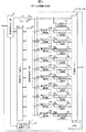
デコード部50は、第1の逆変換部51と、反転データ生成部52と、第2の逆変換部53と、第1〜第10のデータ選択部540〜549と、第1〜第10のCRC演算部550〜559と、非反転データCRC演算部55と、メモリ制御部56と、記憶部としてのメモリ57等とを有している。このうち、第1の逆変換部51、反転データ生成部52、及び第2の逆変換部53は、本発明の逆変換部の一例である。また、第1〜第10のCRC演算部550〜559、非反転データCRC演算部55、及びメモリ制御部56は、本発明の抽出部の一例である。
The
第1の逆変換部51は、DCバランス変換テーブル500を参照し、受信部41から取得した10ビットのパラレルデータを1つのデータ単位として順次DCバランス逆変換を行う。DCバランス変換テーブル500には、送信装置2のDCバランス変換部24が参照する変換テーブルに対応する内容が予め設定されている。
The first
第1の逆変換部51は、DCバランス逆変換された8ビットのデータを出力データD0としてデータバス511に出力する。また、第1の逆変換部51は、受信部41から取得した10ビットのデータに対応する8ビットのデータがDCバランス変換テーブル510に登録されていなかった場合(逆変換が不可能であった場合)には、予め定められた値(例えば「00000000」)の8ビットデータを出力データD0としてデータバス511出力するとともに、逆変換エラーがあったことを示すエラー信号Errを信号線512に出力する。このエラー信号Errは、第1の逆変換部51が上記予め定められた値を出力している間だけオン状態に維持される。
The first
またさらに、第1の逆変換部51は、DCバランス変換前の10ビットのデータ(受信部41から取得したデータ)を10ビットのデータバス513に出力する。
Furthermore, the first
反転データ生成部52は、データバス513を介して受信部41がパラレルデータに変換した10ビットのデータを取得し、この10ビットのデータの第1ビット(最下位ビット)から第10ビット(最上位ビット)の各1ビットを反転した10個の10ビットからなる反転データを生成する。
The inverted
第2の逆変換部53は、反転データ生成部52が生成した10個の反転データのそれぞれについて、DCバランス変換テーブル500を参照してDCバランス逆変換を行い、各反転データに対応する10個の8ビットのデータを生成する。
The second
第1〜第10のデータ選択部540〜549には、第1の逆変換部51がデータバス511に出力する第1の逆変換データ、第2の逆変換部53が出力する第1〜第10ビットの何れか1つが反転された反転データをそれぞれ逆変換した第2の逆変換データ、及び第1の逆変換部51が信号線512に出力するエラー信号Errが入力される。第1のデータ選択部540には、第1ビットが反転された反転データを逆変換した第2の逆変換データが入力され、以下同様に、第2のデータ変換部541には第2ビットが、第3のデータ変換部543には第3ビットが(以下省略)、それぞれ反転された反転データを逆変換した第2の逆変換データが入力される。
The first to tenth
第1〜第10のデータ選択部540〜549は、エラー信号Errがオフ状態である場合には、第1の逆変換データを出力データD1〜D10として出力し、エラー信号Errがオン状態である場合には、第2の逆変換データを出力データD1〜D10として出力する。
When the error signal Err is in the off state, the first to tenth
つまり、第1〜第10のデータ選択部540〜549は、第1の逆変換部51における逆変換が不可能で、第1の逆変換データとして上記予め定められた値が出力されている間は第2の逆変換データを出力し、第1の逆変換部51における逆変換が可能であった場合には第1の逆変換データを出力する。
That is, the first to tenth
これらの出力データD1〜D10は、第1〜第10のCRC演算部550〜559、及びメモリ制御部56に入力される。
The output data D1 to D10 are input to the first to tenth CRC calculation units 550 to 559 and the
第1〜第10のCRC演算部550〜559は、第1〜第10のデータ選択部540〜549から出力された第1又は第2の逆変換データに基づいて、誤り検出符号としてのCRCコードを順次演算し、メモリ制御部56に出力する。
The first to tenth CRC calculation units 550 to 559 are CRC codes as error detection codes based on the first or second inverse transform data output from the first to tenth
また、非反転データCRC演算部55は、データバス511に接続され、第1の逆変換部51が出力した第1の逆変換データのCRCコードを順次演算し、メモリ制御部56に出力する。
The non-inverted data
非反転データCRC演算部55及び第1〜第10のCRC演算部550〜559は、出力データD0〜D10の変化の周期よりも1周期分遅れて、CRCコードをメモリ制御部56に出力するように構成されている。
The non-inverted data
メモリ制御部56は、第1の逆変換部51からの出力データD0、及び第1〜第10のデータ選択部540〜549から出力される出力データD1〜D10をメモリ57のそれぞれ異なる記憶領域に順次記憶する。
The
また、メモリ制御部56は、第1の逆変換部51において逆変換された誤り検出符号としてのCRCコード(受信部31が受信したパケットに含まれるCRCコード)を取得したとき、この取得したCRCコード(以下このCRCコードを「受信CRCコード」という)と、非反転データCRC演算部55から入力されたCRCコードとが一致するかを判定する。この判定の結果、両CRCコードが一致すれば、メモリ57から出力データD0を順次記憶した一連のデータを読み出し、後段のメモリインタフェース42に出力する。
Further, when the
一方、受信CRCコードと非反転データCRC演算部55から入力されたCRCコードとが一致しなかった場合、メモリ制御部56は、第1〜第10のCRC演算部550〜559から入力されたCRCコードのうち、受信CRCコードと一致するものがあるか照合する。この照合の結果一致するものがあれば、第1〜第10のデータ選択部540〜549の出力データD1〜D10のうち、受信CRCコードと一致したCRCコードに対応する出力データを順次記憶した一連のデータをメモリ57から読み出し、誤り訂正された転送データとして後段のメモリインタフェース42に出力する。
On the other hand, if the received CRC code and the CRC code input from the non-inverted data
例えば、第4のCRC演算部553から入力されたCRCコードが受信CRCコードと一致すれば、第4のデータ選択部543の出力データD4を順次記憶した一連のデータをメモリ57から読み出し、後段のメモリインタフェース42に出力する。
For example, if the CRC code input from the fourth
また、メモリ制御部56は、第1〜第10のCRC演算部550〜559から入力されたCRCコードに受信CRCコードと一致するものがない場合、メモリインタフェース42へのデータの出力は行わず、送信装置2にパケットの再送信を要求するための再送要求信号を出力する。
Further, the
なお、メモリ制御部56は、受信CRCコードと非反転データCRC演算部55から入力されたCRCコードとの照合を行わず、第1〜第10のCRC演算部550〜559から入力されたCRCコードのうち、受信CRCコードと一致するものに対応する第1〜第10のデータ選択部540〜549の出力データD1〜D10の何れか1つの出力データを順次記憶したデータをメモリインタフェース42に出力するように構成してもよい。このように構成しても、受信部41が受信した受信データに誤りがない場合には、第1〜第10のCRC演算部550〜559から入力されたCRCコードが全て受信CRCコードと一致するので、正しいデータが出力される。また、このように構成した場合には、非反転データCRC演算部55を省略することができる。
The
(デコード部の動作)
図4は、送信装置2から受信した転送データのうち、2バイト目のデータd2が逆変換不可能であった場合のエラー信号Err、第1の逆変換部51の出力データD0、及び第1〜第10のデータ選択部540〜549の出力データD1〜D10の変化の一例を示すタイミングチャートである。
(Decode operation)
FIG. 4 shows the error signal Err, the output data D0 of the first
エラー信号Errがオンした状態では、第1〜第10のデータ選択部540〜549は、1ビット反転及び逆変換処理された第2の逆変換データを出力するので、出力データD0にデータd2が表れているときに、出力データD1〜D10には第1〜第10ビットがそれぞれ反転したデータd21〜d210が表れる。エラー信号Errがオフした状態では、出力データD0と同一のデータが第1〜第10のデータ選択部540〜549の出力データD1〜D10に表れる。
In a state in which the error signal Err is turned on, the first to tenth
図5は、誤り訂正手段321cによる誤り訂正の具体例を示す図であり、(a)は送信装置2が送信した送信データ及び受信装置3で受信した受信データのうちの10ビットを、(b)はDCバランス逆変換でエラーが発生した10ビットデータの各1ビットを反転したデータ及びそれに対応する8ビットデータを示す。
FIG. 5 is a diagram showing a specific example of error correction by the error correction unit 321c. FIG. 5A shows 10 bits of the transmission data transmitted by the
図5(a)に示すように、送信データは「0010111011」であるのに対し、受信データは「0010110011」であり、第4ビットに誤りが発生している。この場合には、第1の逆変換部51による逆変換が不可能であり、エラー信号Errが1周期分オン状態となる。
As shown in FIG. 5A, the transmission data is “0010111011”, whereas the reception data is “0010110011”, and an error occurs in the fourth bit. In this case, the reverse conversion by the first
図5(b)に示すように、反転データ生成部52は、この10ビットのデータの第1ビットから第10ビットのうちの1ビットをそれぞれ反転した10個の反転データを生成する。また、第2の逆変換部53は、DCバランス変換テーブル500を参照してこれらの反転データを逆変換し、第1〜第10のデータ選択部540〜549に出力する。DCバランス変換テーブル500で対応する8ビットデータが得られない場合には、予め定められた値(図5(b)に示す例では「0」)を第1〜第10のデータ選択部540〜549に出力する。
As shown in FIG. 5B, the inverted
この結果、エラー信号Errがオンしているタイミングでは、図5(b)の右欄に示す各データ(10進数表記)が出力データD1〜D10として表れる。このうち、第4ビットが反転及び逆変換された出力データD4が送信データに対応したデータであるので、第4のCRC演算部553が出力するCRCデータと受信CRCデータとが一致し、第4のデータ選択部543が順次出力してメモリ57に記憶された一連のデータが、誤り訂正された転送データとしてメモリインタフェース42に出力される。
As a result, at the timing when the error signal Err is turned on, each data (decimal notation) shown in the right column of FIG. 5B appears as output data D1 to D10. Among these, since the output data D4 in which the fourth bit is inverted and inversely converted is data corresponding to the transmission data, the CRC data output from the fourth
[他の実施の形態]
なお、本発明は、上記第1の実施の形態に限定されず、その要旨を変更しない範囲内で種々な変形が可能である。
[Other embodiments]
In addition, this invention is not limited to the said 1st Embodiment, A various deformation | transformation is possible within the range which does not change the summary.
例えば、第1の実施の形態では、反転データ生成部52が、10ビットのうちの1ビットを反転した複数の反転データを生成したが、10ビットのうちの1ビット及び2ビットを反転した複数(55個)の反転データを生成し、これらに対応して第2の逆変換部、データ選択部、及びCRC演算部を設けてもよい。またさらに、3ビット以上を反転するようにデコード部を構成してもよい。
For example, in the first embodiment, the inverted
また、第1の実施の形態では、送信装置2で8B/10B変換を行い、受信装置4で8B/10B逆変換を行う場合について説明したが、これに限らず、例えば送信装置2で予め定められた手順に基づく暗号化する変換処理を行い、受信装置4では、送信装置2における暗号化手順に対応して予め定められた複合化手順によって逆変換を行うようにしてもよい。
In the first embodiment, the case where the
また、第1の実施の形態では、ASIC等のハードウェアによってデコード部50を構成した場合について説明したが、これに限らず、予め記憶されたプログラムに従って動作するCPU(Central Processing Unit:演算処理装置)の処理によって、上記説明したデコード部50の各部の機能を実現してもよい。
In the first embodiment, the case where the
1…データ転送装置、2…送信装置、3…受信装置、4…通信線、10,10A…パケット、11,11A…ヘッダ、12,12A…転送データ、13,13A…CRCコード、14,14A…フッタ、21…メモリインタフェース、22…メモリ、23…検出符号付加部、24…DCバランス変換部、25…送信部、41…受信部、42…メモリインタフェース、43…バッファメモリ、50…デコード部、51…第1の逆変換部、52…反転データ生成部、53…第2の逆変換部、55…非反転データCRC演算部、56…メモリ制御部、57…記憶部、500…DCバランス変換テーブル、540〜549…第1〜第10のデータ選択部、550〜559…第1〜第10のCRC演算部 DESCRIPTION OF SYMBOLS 1 ... Data transfer apparatus, 2 ... Transmission apparatus, 3 ... Reception apparatus, 4 ... Communication line, 10, 10A ... Packet, 11, 11A ... Header, 12, 12A ... Transfer data, 13, 13A ... CRC code, 14, 14A ... Footer, 21 ... Memory interface, 22 ... Memory, 23 ... Detection code adding unit, 24 ... DC balance conversion unit, 25 ... Transmitting unit, 41 ... Receiving unit, 42 ... Memory interface, 43 ... Buffer memory, 50 ... Decoding unit , 51... First inverse transform unit, 52... Inverted data generation unit, 53... Second inverse transform unit, 55... Non-inverted data CRC calculation unit, 56. Conversion table, 540 to 549 ... first to tenth data selection units, 550 to 559 ... first to tenth CRC calculation units
Claims (4)
前記受信部が受信した変換データ及び当該変換データの一部のビットを反転した反転データを予め定められた手順に基づいて逆変換した複数の逆変換データを生成する逆変換部と、
前記複数の逆変換データのうち、前記誤り検出符号に基づく誤り検出処理で誤りが検出されない逆変換データを抽出する抽出部とを備えた受信装置。 A receiver for receiving converted data obtained by converting data including transfer data composed of a plurality of bits and an error detection code for error detection of the transfer data based on a predetermined procedure;
An inverse conversion unit that generates a plurality of inversely converted data obtained by inversely converting the converted data received by the receiving unit and the inverted data obtained by inverting some bits of the converted data based on a predetermined procedure;
A receiving device comprising: an extracting unit that extracts, from among the plurality of inverse transform data, inverse transform data in which an error is not detected by an error detection process based on the error detection code.
複数ビットからなる転送データと前記転送データの誤り検出のための誤り検出符号とを含むデータを生成し、前記生成したデータを予め定められた手順に基づいて変換した変換データを送信する送信装置とを備えたデータ転送装置。
The receiving device according to any one of claims 1 to 3,
A transmitter that generates data including transfer data composed of a plurality of bits and an error detection code for error detection of the transfer data, and transmits the converted data obtained by converting the generated data based on a predetermined procedure; A data transfer device comprising:
Priority Applications (3)
| Application Number | Priority Date | Filing Date | Title |
|---|---|---|---|
| JP2010272421A JP2012124643A (en) | 2010-12-07 | 2010-12-07 | Receiving device and data transfer device |
| US13/103,391 US8699624B2 (en) | 2010-12-07 | 2011-05-09 | Receiving apparatus and data transmission apparatus |
| CN201110166126.2A CN102571268B (en) | 2010-12-07 | 2011-06-16 | Receiving apparatus and data transmission apparatus |
Applications Claiming Priority (1)
| Application Number | Priority Date | Filing Date | Title |
|---|---|---|---|
| JP2010272421A JP2012124643A (en) | 2010-12-07 | 2010-12-07 | Receiving device and data transfer device |
Publications (1)
| Publication Number | Publication Date |
|---|---|
| JP2012124643A true JP2012124643A (en) | 2012-06-28 |
Family
ID=46162224
Family Applications (1)
| Application Number | Title | Priority Date | Filing Date |
|---|---|---|---|
| JP2010272421A Pending JP2012124643A (en) | 2010-12-07 | 2010-12-07 | Receiving device and data transfer device |
Country Status (3)
| Country | Link |
|---|---|
| US (1) | US8699624B2 (en) |
| JP (1) | JP2012124643A (en) |
| CN (1) | CN102571268B (en) |
Families Citing this family (1)
| Publication number | Priority date | Publication date | Assignee | Title |
|---|---|---|---|---|
| US9197291B2 (en) * | 2013-06-17 | 2015-11-24 | Infineon Technologies Ag | Circuit arrangement and method for bidirectional data transmission |
Citations (5)
| Publication number | Priority date | Publication date | Assignee | Title |
|---|---|---|---|---|
| JPH1022839A (en) * | 1996-07-02 | 1998-01-23 | Saitama Nippon Denki Kk | Soft discrimination error-correction decoding method |
| JPH11298335A (en) * | 1998-04-06 | 1999-10-29 | Casio Comput Co Ltd | Error correction circuit |
| JP2000092033A (en) * | 1998-09-14 | 2000-03-31 | Nec Corp | High speed data transmission reception system |
| JP2001186108A (en) * | 1999-12-22 | 2001-07-06 | Nec Corp | Communication terminal |
| JP2005020063A (en) * | 2003-06-23 | 2005-01-20 | Sharp Corp | Error correction device in digital communication terminal |
Family Cites Families (29)
| Publication number | Priority date | Publication date | Assignee | Title |
|---|---|---|---|---|
| US4434459A (en) * | 1980-04-25 | 1984-02-28 | Data General Corporation | Data processing system having instruction responsive apparatus for both a basic and an extended instruction set |
| JP3279624B2 (en) | 1992-02-13 | 2002-04-30 | 富士通株式会社 | 1-bit error correction circuit based on CRC operation |
| US5387911A (en) * | 1992-02-21 | 1995-02-07 | Gleichert; Marc C. | Method and apparatus for transmitting and receiving both 8B/10B code and 10B/12B code in a switchable 8B/10B transmitter and receiver |
| JP2715900B2 (en) | 1994-03-30 | 1998-02-18 | 日本電気株式会社 | Parallel data transmission equipment |
| JPH1013251A (en) | 1996-06-25 | 1998-01-16 | Saitama Nippon Denki Kk | Code error-correction circuit |
| US6389572B1 (en) * | 1999-05-28 | 2002-05-14 | Palm, Inc. | Method of extracting bits from modulated waveforms |
| US6956852B1 (en) * | 1999-06-25 | 2005-10-18 | Cisco Technology Inc. | Multi-function high-speed network interface |
| JP3839215B2 (en) * | 2000-03-14 | 2006-11-01 | 株式会社日立製作所 | Error detection / correction method, main storage controller for computer system, and computer system |
| US20030016758A1 (en) * | 2001-07-05 | 2003-01-23 | David Wu | Universal interface to external transceiver |
| JP3879836B2 (en) * | 2002-03-28 | 2007-02-14 | 日本電気株式会社 | Multiplex converter, demultiplexer, and multiplex transmission system |
| US20030235298A1 (en) * | 2002-06-25 | 2003-12-25 | Bedros Hanounik | Shifting an encryption key in either a first or second direction via a uni-directional shifting unit |
| JP2004147041A (en) * | 2002-10-24 | 2004-05-20 | Mitsubishi Electric Corp | Detection circuit and decoding circuit |
| US7103830B1 (en) * | 2002-12-18 | 2006-09-05 | Applied Micro Circuits Corporation | DC balanced error correction coding |
| US7047475B2 (en) * | 2003-02-04 | 2006-05-16 | Hewlett-Packard Development Company, L.P. | CRC encoding scheme for conveying status information |
| JP3822632B2 (en) * | 2004-04-16 | 2006-09-20 | ザインエレクトロニクス株式会社 | Transmission circuit, reception circuit, clock extraction circuit, data transmission method and data transmission system |
| US7183797B2 (en) * | 2004-10-29 | 2007-02-27 | Altera Corporation | Next generation 8B10B architecture |
| FI117780B (en) * | 2005-03-15 | 2007-02-15 | Elektrobit Testing Oy | Method and Test Arrangements for Testing a Device Using 8B / 10B Encoding and 8B / 10B Encoder and Decoder |
| JP4612864B2 (en) * | 2005-05-19 | 2011-01-12 | キヤノン株式会社 | Communication device, reception method, codec, decoder, communication module, communication unit, and decoding method in the device |
| JP2007207325A (en) * | 2006-01-31 | 2007-08-16 | Toshiba Corp | Error correction processing apparatus and error correction processing method |
| US7802167B1 (en) * | 2006-02-08 | 2010-09-21 | Pmc-Sierra Us, Inc. | Apparatus and method for detecting extended error bursts |
| JP4684185B2 (en) * | 2006-08-15 | 2011-05-18 | 富士通株式会社 | Communications system |
| US8560920B2 (en) * | 2006-10-05 | 2013-10-15 | Freescale Semiconductor, Inc. | Error correction via lookup in compressed error location data |
| US8103942B2 (en) | 2007-05-24 | 2012-01-24 | Fuji Xerox Co., Ltd. | Data transmission apparatus, data transmission device, data reception device and data transmission system |
| JP5233165B2 (en) | 2007-05-24 | 2013-07-10 | 富士ゼロックス株式会社 | Data transmission device |
| WO2010027136A1 (en) * | 2008-09-03 | 2010-03-11 | Lg Electronics Inc. | Realy station and method of operating the same |
| US8514955B2 (en) * | 2009-03-24 | 2013-08-20 | Megachips Corporation | Communication system, data transmitter, and data receiver capable of detecting incorrect receipt of data |
| JP2010225239A (en) * | 2009-03-24 | 2010-10-07 | Toshiba Corp | Semiconductor integrated circuit and memory functional verification method |
| JP2011052987A (en) * | 2009-08-31 | 2011-03-17 | Casio Computer Co Ltd | Positioning data receiver, error correction device, and program |
| US8432729B2 (en) * | 2010-04-13 | 2013-04-30 | Mosaid Technologies Incorporated | Phase-change memory with multiple polarity bits having enhanced endurance and error tolerance |
-
2010
- 2010-12-07 JP JP2010272421A patent/JP2012124643A/en active Pending
-
2011
- 2011-05-09 US US13/103,391 patent/US8699624B2/en not_active Expired - Fee Related
- 2011-06-16 CN CN201110166126.2A patent/CN102571268B/en active Active
Patent Citations (5)
| Publication number | Priority date | Publication date | Assignee | Title |
|---|---|---|---|---|
| JPH1022839A (en) * | 1996-07-02 | 1998-01-23 | Saitama Nippon Denki Kk | Soft discrimination error-correction decoding method |
| JPH11298335A (en) * | 1998-04-06 | 1999-10-29 | Casio Comput Co Ltd | Error correction circuit |
| JP2000092033A (en) * | 1998-09-14 | 2000-03-31 | Nec Corp | High speed data transmission reception system |
| JP2001186108A (en) * | 1999-12-22 | 2001-07-06 | Nec Corp | Communication terminal |
| JP2005020063A (en) * | 2003-06-23 | 2005-01-20 | Sharp Corp | Error correction device in digital communication terminal |
Also Published As
| Publication number | Publication date |
|---|---|
| CN102571268B (en) | 2017-04-12 |
| US20120140855A1 (en) | 2012-06-07 |
| CN102571268A (en) | 2012-07-11 |
| US8699624B2 (en) | 2014-04-15 |
Similar Documents
| Publication | Publication Date | Title |
|---|---|---|
| TWI459774B (en) | Asynchronous master-slave serial communication systam, data transmission method, and control module using the same thereof | |
| JP2715900B2 (en) | Parallel data transmission equipment | |
| JP2008294757A (en) | Data transmitting apparatus, data sending apparatus, data receiving apparatus and data transmission system | |
| TWI518500B (en) | Data transmission detecing device, data transmission detecing method and electronic device thereof | |
| JP4260688B2 (en) | Data transmission device, data transmission / reception system, data transmission device control method, and data transmission / reception system control method | |
| CN102469313B (en) | Coding apparatus, coding method, decoding apparatus, decoding method and transmission system | |
| CN106210749A (en) | Decoding device, information transmission system and coding/decoding method | |
| CN101304358B (en) | Transmitter, receiver, transmitting method, receiving method, and semiconductor device | |
| CN103199876A (en) | Method and device for achieving soft-decision forward error correction (FEC) decoding | |
| US8750423B2 (en) | Receiving apparatus, data transfer apparatus, data receiving method and non-transitory computer readable recording medium | |
| JP2013058845A (en) | Data communication method and data communication system | |
| JP2012124643A (en) | Receiving device and data transfer device | |
| US8621314B2 (en) | Transmitting and receiving system and method, and non-transitory computer readable medium | |
| CN113938242A (en) | Retransmission method and communication device | |
| JP2009141453A (en) | Data transmission device, data transmission device, data reception device, and data transmission system | |
| JP7540166B2 (en) | Transmitting device, receiving device, transmitting method, and receiving method | |
| CN106849961A (en) | A kind of forward error correction circuit, high speed serialization transceiver and PLD | |
| CN111130695A (en) | A Method of Calculating CRC of CANOPEN Protocol by Redundant Code Words | |
| JP2013255054A (en) | Transmitting and receiving system and program | |
| US20090150727A1 (en) | Data transmission method | |
| JP2010068264A (en) | Digital signal conversion apparatus | |
| KR20100064442A (en) | Encoding/decoding method and device using the same | |
| JP2009065255A (en) | Data transmission apparatus, data transmission device, data reception device, and data transmission system | |
| Krishnapriya et al. | Design and Simulation of SIE with Error Correction Mechanism in 45nm Technology | |
| CN113904754A (en) | A kind of CRC error correction method and related device |
Legal Events
| Date | Code | Title | Description |
|---|---|---|---|
| A621 | Written request for application examination |
Free format text: JAPANESE INTERMEDIATE CODE: A621 Effective date: 20131121 |
|
| A977 | Report on retrieval |
Free format text: JAPANESE INTERMEDIATE CODE: A971007 Effective date: 20140828 |
|
| A131 | Notification of reasons for refusal |
Free format text: JAPANESE INTERMEDIATE CODE: A131 Effective date: 20140902 |
|
| A521 | Written amendment |
Free format text: JAPANESE INTERMEDIATE CODE: A523 Effective date: 20141030 |
|
| A02 | Decision of refusal |
Free format text: JAPANESE INTERMEDIATE CODE: A02 Effective date: 20150310 |