JP2012146919A - 半導体モジュール - Google Patents
半導体モジュール Download PDFInfo
- Publication number
- JP2012146919A JP2012146919A JP2011005961A JP2011005961A JP2012146919A JP 2012146919 A JP2012146919 A JP 2012146919A JP 2011005961 A JP2011005961 A JP 2011005961A JP 2011005961 A JP2011005961 A JP 2011005961A JP 2012146919 A JP2012146919 A JP 2012146919A
- Authority
- JP
- Japan
- Prior art keywords
- region
- metal block
- plating
- semiconductor element
- metal
- Prior art date
- Legal status (The legal status is an assumption and is not a legal conclusion. Google has not performed a legal analysis and makes no representation as to the accuracy of the status listed.)
- Granted
Links
Images


Classifications
-
- H—ELECTRICITY
- H10—SEMICONDUCTOR DEVICES; ELECTRIC SOLID-STATE DEVICES NOT OTHERWISE PROVIDED FOR
- H10W—GENERIC PACKAGES, INTERCONNECTIONS, CONNECTORS OR OTHER CONSTRUCTIONAL DETAILS OF DEVICES COVERED BY CLASS H10
- H10W40/00—Arrangements for thermal protection or thermal control
- H10W40/70—Fillings or auxiliary members in containers or in encapsulations for thermal protection or control
- H10W40/77—Auxiliary members characterised by their shape
- H10W40/778—Auxiliary members characterised by their shape in encapsulations
-
- H—ELECTRICITY
- H10—SEMICONDUCTOR DEVICES; ELECTRIC SOLID-STATE DEVICES NOT OTHERWISE PROVIDED FOR
- H10W—GENERIC PACKAGES, INTERCONNECTIONS, CONNECTORS OR OTHER CONSTRUCTIONAL DETAILS OF DEVICES COVERED BY CLASS H10
- H10W40/00—Arrangements for thermal protection or thermal control
- H10W40/40—Arrangements for thermal protection or thermal control involving heat exchange by flowing fluids
- H10W40/47—Arrangements for thermal protection or thermal control involving heat exchange by flowing fluids by flowing liquids, e.g. forced water cooling
-
- H—ELECTRICITY
- H10—SEMICONDUCTOR DEVICES; ELECTRIC SOLID-STATE DEVICES NOT OTHERWISE PROVIDED FOR
- H10W—GENERIC PACKAGES, INTERCONNECTIONS, CONNECTORS OR OTHER CONSTRUCTIONAL DETAILS OF DEVICES COVERED BY CLASS H10
- H10W72/00—Interconnections or connectors in packages
- H10W72/60—Strap connectors, e.g. thick copper clips for grounding of power devices
-
- H—ELECTRICITY
- H10—SEMICONDUCTOR DEVICES; ELECTRIC SOLID-STATE DEVICES NOT OTHERWISE PROVIDED FOR
- H10W—GENERIC PACKAGES, INTERCONNECTIONS, CONNECTORS OR OTHER CONSTRUCTIONAL DETAILS OF DEVICES COVERED BY CLASS H10
- H10W74/00—Encapsulations, e.g. protective coatings
- H10W74/10—Encapsulations, e.g. protective coatings characterised by their shape or disposition
- H10W74/111—Encapsulations, e.g. protective coatings characterised by their shape or disposition the semiconductor body being completely enclosed
- H10W74/127—Encapsulations, e.g. protective coatings characterised by their shape or disposition the semiconductor body being completely enclosed characterised by arrangements for sealing or adhesion
-
- H—ELECTRICITY
- H10—SEMICONDUCTOR DEVICES; ELECTRIC SOLID-STATE DEVICES NOT OTHERWISE PROVIDED FOR
- H10W—GENERIC PACKAGES, INTERCONNECTIONS, CONNECTORS OR OTHER CONSTRUCTIONAL DETAILS OF DEVICES COVERED BY CLASS H10
- H10W70/00—Package substrates; Interposers; Redistribution layers [RDL]
- H10W70/20—Conductive package substrates serving as an interconnection, e.g. metal plates
-
- H—ELECTRICITY
- H10—SEMICONDUCTOR DEVICES; ELECTRIC SOLID-STATE DEVICES NOT OTHERWISE PROVIDED FOR
- H10W—GENERIC PACKAGES, INTERCONNECTIONS, CONNECTORS OR OTHER CONSTRUCTIONAL DETAILS OF DEVICES COVERED BY CLASS H10
- H10W72/00—Interconnections or connectors in packages
- H10W72/01—Manufacture or treatment
- H10W72/013—Manufacture or treatment of die-attach connectors
- H10W72/01308—Manufacture or treatment of die-attach connectors using permanent auxiliary members, e.g. using alignment marks
-
- H—ELECTRICITY
- H10—SEMICONDUCTOR DEVICES; ELECTRIC SOLID-STATE DEVICES NOT OTHERWISE PROVIDED FOR
- H10W—GENERIC PACKAGES, INTERCONNECTIONS, CONNECTORS OR OTHER CONSTRUCTIONAL DETAILS OF DEVICES COVERED BY CLASS H10
- H10W72/00—Interconnections or connectors in packages
- H10W72/071—Connecting or disconnecting
- H10W72/073—Connecting or disconnecting of die-attach connectors
- H10W72/07331—Connecting techniques
- H10W72/07336—Soldering or alloying
-
- H—ELECTRICITY
- H10—SEMICONDUCTOR DEVICES; ELECTRIC SOLID-STATE DEVICES NOT OTHERWISE PROVIDED FOR
- H10W—GENERIC PACKAGES, INTERCONNECTIONS, CONNECTORS OR OTHER CONSTRUCTIONAL DETAILS OF DEVICES COVERED BY CLASS H10
- H10W72/00—Interconnections or connectors in packages
- H10W72/071—Connecting or disconnecting
- H10W72/076—Connecting or disconnecting of strap connectors
- H10W72/07631—Techniques
- H10W72/07636—Soldering or alloying
-
- H—ELECTRICITY
- H10—SEMICONDUCTOR DEVICES; ELECTRIC SOLID-STATE DEVICES NOT OTHERWISE PROVIDED FOR
- H10W—GENERIC PACKAGES, INTERCONNECTIONS, CONNECTORS OR OTHER CONSTRUCTIONAL DETAILS OF DEVICES COVERED BY CLASS H10
- H10W72/00—Interconnections or connectors in packages
- H10W72/071—Connecting or disconnecting
- H10W72/076—Connecting or disconnecting of strap connectors
- H10W72/07651—Connecting or disconnecting of strap connectors characterised by changes in properties of the strap connectors during connecting
- H10W72/07653—Connecting or disconnecting of strap connectors characterised by changes in properties of the strap connectors during connecting changes in shapes
-
- H—ELECTRICITY
- H10—SEMICONDUCTOR DEVICES; ELECTRIC SOLID-STATE DEVICES NOT OTHERWISE PROVIDED FOR
- H10W—GENERIC PACKAGES, INTERCONNECTIONS, CONNECTORS OR OTHER CONSTRUCTIONAL DETAILS OF DEVICES COVERED BY CLASS H10
- H10W72/00—Interconnections or connectors in packages
- H10W72/30—Die-attach connectors
- H10W72/351—Materials of die-attach connectors
- H10W72/352—Materials of die-attach connectors comprising metals or metalloids, e.g. solders
-
- H—ELECTRICITY
- H10—SEMICONDUCTOR DEVICES; ELECTRIC SOLID-STATE DEVICES NOT OTHERWISE PROVIDED FOR
- H10W—GENERIC PACKAGES, INTERCONNECTIONS, CONNECTORS OR OTHER CONSTRUCTIONAL DETAILS OF DEVICES COVERED BY CLASS H10
- H10W72/00—Interconnections or connectors in packages
- H10W72/50—Bond wires
- H10W72/551—Materials of bond wires
- H10W72/552—Materials of bond wires comprising metals or metalloids, e.g. silver
- H10W72/5524—Materials of bond wires comprising metals or metalloids, e.g. silver comprising aluminium [Al]
-
- H—ELECTRICITY
- H10—SEMICONDUCTOR DEVICES; ELECTRIC SOLID-STATE DEVICES NOT OTHERWISE PROVIDED FOR
- H10W—GENERIC PACKAGES, INTERCONNECTIONS, CONNECTORS OR OTHER CONSTRUCTIONAL DETAILS OF DEVICES COVERED BY CLASS H10
- H10W72/00—Interconnections or connectors in packages
- H10W72/851—Dispositions of multiple connectors or interconnections
- H10W72/853—On the same surface
- H10W72/871—Bond wires and strap connectors
-
- H—ELECTRICITY
- H10—SEMICONDUCTOR DEVICES; ELECTRIC SOLID-STATE DEVICES NOT OTHERWISE PROVIDED FOR
- H10W—GENERIC PACKAGES, INTERCONNECTIONS, CONNECTORS OR OTHER CONSTRUCTIONAL DETAILS OF DEVICES COVERED BY CLASS H10
- H10W72/00—Interconnections or connectors in packages
- H10W72/851—Dispositions of multiple connectors or interconnections
- H10W72/874—On different surfaces
- H10W72/884—Die-attach connectors and bond wires
-
- H—ELECTRICITY
- H10—SEMICONDUCTOR DEVICES; ELECTRIC SOLID-STATE DEVICES NOT OTHERWISE PROVIDED FOR
- H10W—GENERIC PACKAGES, INTERCONNECTIONS, CONNECTORS OR OTHER CONSTRUCTIONAL DETAILS OF DEVICES COVERED BY CLASS H10
- H10W72/00—Interconnections or connectors in packages
- H10W72/90—Bond pads, in general
- H10W72/931—Shapes of bond pads
-
- H—ELECTRICITY
- H10—SEMICONDUCTOR DEVICES; ELECTRIC SOLID-STATE DEVICES NOT OTHERWISE PROVIDED FOR
- H10W—GENERIC PACKAGES, INTERCONNECTIONS, CONNECTORS OR OTHER CONSTRUCTIONAL DETAILS OF DEVICES COVERED BY CLASS H10
- H10W72/00—Interconnections or connectors in packages
- H10W72/90—Bond pads, in general
- H10W72/941—Dispositions of bond pads
- H10W72/944—Dispositions of multiple bond pads
-
- H—ELECTRICITY
- H10—SEMICONDUCTOR DEVICES; ELECTRIC SOLID-STATE DEVICES NOT OTHERWISE PROVIDED FOR
- H10W—GENERIC PACKAGES, INTERCONNECTIONS, CONNECTORS OR OTHER CONSTRUCTIONAL DETAILS OF DEVICES COVERED BY CLASS H10
- H10W74/00—Encapsulations, e.g. protective coatings
-
- H—ELECTRICITY
- H10—SEMICONDUCTOR DEVICES; ELECTRIC SOLID-STATE DEVICES NOT OTHERWISE PROVIDED FOR
- H10W—GENERIC PACKAGES, INTERCONNECTIONS, CONNECTORS OR OTHER CONSTRUCTIONAL DETAILS OF DEVICES COVERED BY CLASS H10
- H10W90/00—Package configurations
-
- H—ELECTRICITY
- H10—SEMICONDUCTOR DEVICES; ELECTRIC SOLID-STATE DEVICES NOT OTHERWISE PROVIDED FOR
- H10W—GENERIC PACKAGES, INTERCONNECTIONS, CONNECTORS OR OTHER CONSTRUCTIONAL DETAILS OF DEVICES COVERED BY CLASS H10
- H10W90/00—Package configurations
- H10W90/701—Package configurations characterised by the relative positions of pads or connectors relative to package parts
- H10W90/731—Package configurations characterised by the relative positions of pads or connectors relative to package parts of die-attach connectors
- H10W90/736—Package configurations characterised by the relative positions of pads or connectors relative to package parts of die-attach connectors between a chip and a stacked lead frame, conducting package substrate or heat sink
-
- H—ELECTRICITY
- H10—SEMICONDUCTOR DEVICES; ELECTRIC SOLID-STATE DEVICES NOT OTHERWISE PROVIDED FOR
- H10W—GENERIC PACKAGES, INTERCONNECTIONS, CONNECTORS OR OTHER CONSTRUCTIONAL DETAILS OF DEVICES COVERED BY CLASS H10
- H10W90/00—Package configurations
- H10W90/701—Package configurations characterised by the relative positions of pads or connectors relative to package parts
- H10W90/751—Package configurations characterised by the relative positions of pads or connectors relative to package parts of bond wires
- H10W90/756—Package configurations characterised by the relative positions of pads or connectors relative to package parts of bond wires between a chip and a stacked lead frame, conducting package substrate or heat sink
-
- H—ELECTRICITY
- H10—SEMICONDUCTOR DEVICES; ELECTRIC SOLID-STATE DEVICES NOT OTHERWISE PROVIDED FOR
- H10W—GENERIC PACKAGES, INTERCONNECTIONS, CONNECTORS OR OTHER CONSTRUCTIONAL DETAILS OF DEVICES COVERED BY CLASS H10
- H10W90/00—Package configurations
- H10W90/701—Package configurations characterised by the relative positions of pads or connectors relative to package parts
- H10W90/761—Package configurations characterised by the relative positions of pads or connectors relative to package parts of strap connectors
- H10W90/764—Package configurations characterised by the relative positions of pads or connectors relative to package parts of strap connectors between a chip and a stacked insulating package substrate, interposer or RDL
-
- H—ELECTRICITY
- H10—SEMICONDUCTOR DEVICES; ELECTRIC SOLID-STATE DEVICES NOT OTHERWISE PROVIDED FOR
- H10W—GENERIC PACKAGES, INTERCONNECTIONS, CONNECTORS OR OTHER CONSTRUCTIONAL DETAILS OF DEVICES COVERED BY CLASS H10
- H10W95/00—Packaging processes not covered by the other groups of this subclass
Landscapes
- Structures Or Materials For Encapsulating Or Coating Semiconductor Devices Or Solid State Devices (AREA)
- Cooling Or The Like Of Semiconductors Or Solid State Devices (AREA)
- Encapsulation Of And Coatings For Semiconductor Or Solid State Devices (AREA)
Abstract
【解決手段】本半導体モジュールは、金属ブロックと、前記金属ブロックの一方の面に設けられた半導体素子設置領域にはんだ層を介して設置された半導体素子と、前記金属ブロック及び前記半導体素子に樹脂をモールドして形成されるモールド部と、を有し、前記金属ブロックの一方の面は、めっき領域と、粗化領域と、を含み、前記半導体素子設置領域は、前記めっき領域に設けられている。
【選択図】図6
Description
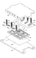
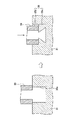
図1は、本発明の第1の実施の形態に係る半導体モジュール1の外観を例示する斜視図であり、(A)は、上方から見た斜視図であり、(B)は、下方から見た斜視図である。尚、搭載状態に応じて上下方向が異なるが、以下では、便宜上、半導体モジュール1の冷却板側を下方とする。また、用語の定義として、「中心側」または「中央側」とは、半導体モジュール1の中心O(図1(A)参照)を基準とする。尚、中心Oは凡そであればよく、厳密に決定されるべき性質のものでない。図2は、図1の半導体モジュール1の要部要素を便宜上分解して例示する分解斜視図である。
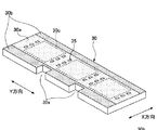
第2の実施の形態では、第1の実施の形態に係る金属ブロック30とは異なる粗化領域を設けた金属ブロック30Aを例示する。なお、第2の実施の形態において、既に説明した実施の形態と同一構成部についての説明は省略する。
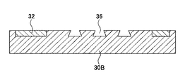
第3の実施の形態では、めっき領域30aに第2の実施の形態とは形状の異なる凹部が設けられた金属ブロック30Bを例示する。なお、第3の実施の形態において、既に説明した実施の形態と同一構成部についての説明は省略する。
第4の実施の形態では、第1の実施の形態に係る金属ブロック30とは異なるめっき領域及び粗化領域を設けた金属ブロック30Cを例示する。なお、第4の実施の形態において、既に説明した実施の形態と同一構成部についての説明は省略する。
第5の実施の形態では、第1の実施の形態に係る金属ブロック30、第2の実施の形態に係る金属ブロック30A、第3の実施の形態に係る金属ブロック30B、又は第4の実施の形態に係る金属ブロック30Cを備えた半導体モジュール1を含むハイブリッドシステムを例示する。なお、第5の実施の形態において、既に説明した実施の形態と同一構成部についての説明は省略する。
10 半導体素子
20 配線部材
20a 端子
22 配線部材
22a 端子
30,30A,30B,30C 金属ブロック
30a,30d,31a めっき領域
30b,30e,31b,32b 粗化領域
30c 半導体素子設置領域
30x 切り欠き部
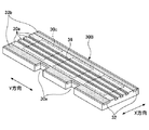
31 フープ材
32 金属板
35,36,37 凹部
35a 楔状部
35b 矩形状部
39 金型
40 絶縁シート
50 冷却板
50a 冷却板の下面
50b 冷却板の側面
50c 冷却板の上面
51 薄肉部
52 締結部
53 締結穴
54 フィン
55 シール部
60 樹脂モールド部
62 延長側部
66 リブ部
80 はんだ層
82 はんだ層
90 ドライブ基板
100 流路形成部材
102 冷却媒体流路
106 ネジ穴
108 シール部
109 支持面
110 ボルト
120 シール材
600 ハイブリッドシステム
602 電池
610 インバータ
612 IPM
616 DC/DC昇圧コンバータ
620,622 モータジェネレータ
Claims (13)
- 金属ブロックと、
前記金属ブロックの一方の面に設けられた半導体素子設置領域にはんだ層を介して設置された半導体素子と、
前記金属ブロック及び前記半導体素子に樹脂をモールドして形成されるモールド部と、を有し、
前記金属ブロックの一方の面は、めっき領域と、粗化領域と、を含み、
前記半導体素子設置領域は、前記めっき領域に設けられている半導体モジュール。 - 前記めっき領域は、前記金属ブロックに対して帯状に形成されている請求項1記載の半導体モジュール。
- 前記めっき領域には複数の凹部が形成されている請求項2記載の半導体モジュール。
- 前記粗化領域は、前記めっき領域の両側に帯状に形成されている請求項2又は3記載の半導体モジュール。
- 前記金属ブロックの一方の面は、前記金属ブロックの一部に圧入された前記金属ブロックとは異なる材料からなる金属板の上面を含み、
前記金属板の上面は粗化領域とされており、
前記金属ブロックの一方の面の前記金属板の上面を除く領域はめっき領域とされている請求項1乃至4の何れ一項記載の半導体モジュール。 - 前記半導体素子設置領域は、前記金属ブロックの一方の面に複数個設けられている請求項1乃至5の何れか一項記載の半導体モジュール。
- 金属ブロックと、前記金属ブロックの一方の面に設けられた半導体素子設置領域にはんだ層を介して設置された半導体素子と、前記金属ブロック及び前記半導体素子に樹脂をモールドして形成されるモールド部と、を有する半導体モジュールの製造方法であって、
複数の半導体素子設置領域が並設された帯状の金属材料を準備し、前記金属材料の一方の面の所定領域にめっきを施し、前記複数の半導体素子設置領域を含むめっき領域を形成する第1工程と、
前記めっき領域をマスクで被覆する第2工程と、
前記金属材料の一方の面の前記マスクから露出する領域を粗化し、粗化領域を形成する第3工程と、
前記金属材料を短手方向に切断して個片化し、前記半導体素子設置領域を少なくとも1つ含む金属ブロックを形成する第4工程と、を有する半導体モジュールの製造方法。 - 前記第1工程よりも前に、前記金属材料の一部に前記金属材料とは異なる材料からなる金属板を圧入し、前記金属板の上面を前記金属材料の一方の面の一部に露出させる工程を更に有し、
前記第1工程では、前記金属材料の一方の面の前記金属板の上面を除く領域に選択的にめっきを施して前記めっき領域を形成する請求項7記載の半導体モジュールの製造方法。 - 前記第1工程よりも前に、前記複数の半導体素子設置領域が並設する帯状の領域を露出するように、前記金属材料の一方の面を第2のマスクで被覆する工程を更に有し、
前記第1工程では、前記金属材料の一方の面の前記第2のマスクから露出する領域にめっきを施して前記めっき領域を形成し、
前記第3工程では、前記第2のマスクを除去した後、前記粗化領域を形成する請求項8記載の半導体モジュールの製造方法。 - 前記めっき領域に複数の凹部を形成する第5工程を更に有する請求項7乃至9の何れか一項記載の半導体モジュールの製造方法。
- 前記金属材料はフープ材である請求項7乃至10の何れか一項記載の半導体モジュールの製造方法。
- 前記マスク及び前記第2のマスクの何れか一方又は双方は、マスクする領域の幅に対応する幅を有する帯状の部材である請求項7乃至11の何れか一項記載の半導体モジュールの製造方法。
- 請求項1〜6の何れか一項記載の半導体モジュールを含むハイブリッドシステム。
Priority Applications (4)
| Application Number | Priority Date | Filing Date | Title |
|---|---|---|---|
| JP2011005961A JP5251991B2 (ja) | 2011-01-14 | 2011-01-14 | 半導体モジュール |
| DE102012100137.5A DE102012100137B4 (de) | 2011-01-14 | 2012-01-10 | Halbleitermodul, Verfahren zur Herstellung desselben und System mit demselben |
| US13/349,993 US8742556B2 (en) | 2011-01-14 | 2012-01-13 | Semiconductor module |
| CN201210013261.8A CN102593091B (zh) | 2011-01-14 | 2012-01-13 | 半导体模块 |
Applications Claiming Priority (1)
| Application Number | Priority Date | Filing Date | Title |
|---|---|---|---|
| JP2011005961A JP5251991B2 (ja) | 2011-01-14 | 2011-01-14 | 半導体モジュール |
Publications (2)
| Publication Number | Publication Date |
|---|---|
| JP2012146919A true JP2012146919A (ja) | 2012-08-02 |
| JP5251991B2 JP5251991B2 (ja) | 2013-07-31 |
Family
ID=46481541
Family Applications (1)
| Application Number | Title | Priority Date | Filing Date |
|---|---|---|---|
| JP2011005961A Expired - Fee Related JP5251991B2 (ja) | 2011-01-14 | 2011-01-14 | 半導体モジュール |
Country Status (4)
| Country | Link |
|---|---|
| US (1) | US8742556B2 (ja) |
| JP (1) | JP5251991B2 (ja) |
| CN (1) | CN102593091B (ja) |
| DE (1) | DE102012100137B4 (ja) |
Cited By (12)
| Publication number | Priority date | Publication date | Assignee | Title |
|---|---|---|---|---|
| JP2014236179A (ja) * | 2013-06-05 | 2014-12-15 | 住友電気工業株式会社 | 半導体モジュール |
| JP2015154634A (ja) * | 2014-02-17 | 2015-08-24 | 株式会社デンソー | 電力変換装置 |
| JP2016025144A (ja) * | 2014-07-17 | 2016-02-08 | イビデン株式会社 | 回路基板及びその製造方法 |
| US9362219B2 (en) | 2013-05-09 | 2016-06-07 | Mitsubishi Electric Corporation | Semiconductor module and semiconductor device |
| US9530713B2 (en) | 2014-06-23 | 2016-12-27 | Fuji Electric Co., Ltd. | Cooler-integrated semiconductor module |
| JPWO2014141346A1 (ja) * | 2013-03-15 | 2017-02-16 | 三菱電機株式会社 | 半導体装置 |
| US10971431B2 (en) | 2018-05-30 | 2021-04-06 | Fuji Electric Co., Ltd. | Semiconductor device, cooling module, power converting device, and electric vehicle |
| US11201121B2 (en) | 2017-04-14 | 2021-12-14 | Fuji Electric Co., Ltd | Semiconductor device |
| WO2022085572A1 (ja) * | 2020-10-19 | 2022-04-28 | パナソニックIpマネジメント株式会社 | 低抵抗部品、回路基板、及び製造方法 |
| JP2023077817A (ja) * | 2021-11-25 | 2023-06-06 | 三菱電機株式会社 | 半導体装置及び電力変換装置 |
| JPWO2024095713A1 (ja) * | 2022-11-04 | 2024-05-10 | ||
| JP2024113030A (ja) * | 2018-08-30 | 2024-08-21 | ローム株式会社 | 半導体装置 |
Families Citing this family (22)
| Publication number | Priority date | Publication date | Assignee | Title |
|---|---|---|---|---|
| US8089150B2 (en) * | 2006-11-14 | 2012-01-03 | Rinehart Lawrence E | Structurally robust power switching assembly |
| US9502329B2 (en) * | 2011-05-16 | 2016-11-22 | Fuji Electric Co., Ltd. | Semiconductor module cooler |
| CN104798185B (zh) * | 2012-11-15 | 2018-04-10 | 日产自动车株式会社 | Au系钎料模片接合半导体装置及其制造方法 |
| USD739349S1 (en) * | 2013-02-12 | 2015-09-22 | IDEMITSU KOGYO Co., LTD. | Current plate for insulation washer for power transformer |
| US11233029B2 (en) | 2013-04-10 | 2022-01-25 | Mitsubishi Electric Corporation | Semiconductor device having a device fixed on a substrate with an adhesive |
| JP2015023211A (ja) * | 2013-07-22 | 2015-02-02 | ローム株式会社 | パワーモジュールおよびその製造方法 |
| DE102013110815B3 (de) * | 2013-09-30 | 2014-10-30 | Semikron Elektronik Gmbh & Co. Kg | Leistungshalbleitereinrichtung und Verfahren zur Herstellung einer Leistungshalbleitereinrichtung |
| US9282649B2 (en) * | 2013-10-08 | 2016-03-08 | Cisco Technology, Inc. | Stand-off block |
| US9148946B1 (en) * | 2014-03-28 | 2015-09-29 | Deere & Company | Electronic assembly for an inverter |
| JP6385234B2 (ja) * | 2014-10-16 | 2018-09-05 | 三菱電機株式会社 | 半導体装置 |
| JP6168082B2 (ja) * | 2015-02-27 | 2017-07-26 | トヨタ自動車株式会社 | 電力変換装置 |
| JP6421055B2 (ja) | 2015-03-05 | 2018-11-07 | 日立オートモティブシステムズ株式会社 | 電力変換装置 |
| EP3166143A1 (fr) * | 2015-11-05 | 2017-05-10 | Gemalto Sa | Procede de fabrication d'un dispositif a puce de circuit integre par depot direct de matiere conductrice |
| CN108369933B (zh) * | 2015-12-16 | 2021-06-29 | 三菱电机株式会社 | 半导体装置及其制造方法 |
| KR102325110B1 (ko) * | 2017-05-31 | 2021-11-11 | 한온시스템 주식회사 | 전기소자 냉각용 열교환기 |
| JP6762271B2 (ja) * | 2017-06-26 | 2020-09-30 | 三菱電機株式会社 | 半導体装置 |
| WO2019012679A1 (ja) * | 2017-07-14 | 2019-01-17 | 新電元工業株式会社 | 電子モジュール |
| JP6522243B1 (ja) * | 2017-07-14 | 2019-05-29 | 新電元工業株式会社 | 電子モジュール |
| JP6560819B1 (ja) * | 2017-11-10 | 2019-08-14 | 新電元工業株式会社 | 電子モジュール及び電子モジュールの製造方法 |
| US11227810B2 (en) * | 2017-11-10 | 2022-01-18 | Shindengen Electric Manufacturing Co., Ltd. | Electronic module with a groove and press hole on the surface of a conductor |
| DE112017008226T5 (de) * | 2017-11-22 | 2020-09-03 | Mitsubishi Electric Corporation | Halbleitervorrichtung |
| CN111433910B (zh) | 2017-12-13 | 2023-10-10 | 三菱电机株式会社 | 半导体装置以及半导体装置的制造方法 |
Citations (4)
| Publication number | Priority date | Publication date | Assignee | Title |
|---|---|---|---|---|
| JPS5245368U (ja) * | 1975-09-27 | 1977-03-31 | ||
| JPH01102947A (ja) * | 1987-10-15 | 1989-04-20 | Hitachi Ltd | 樹脂封止型半導体デバイスおよびリードフレーム |
| WO1998024128A1 (en) * | 1996-11-28 | 1998-06-04 | Mitsubishi Denki Kabushiki Kaisha | Semiconductor device |
| JP2010267730A (ja) * | 2009-05-13 | 2010-11-25 | Hitachi Cable Precision Co Ltd | リードフレーム、半導体装置、及びリードフレームの製造方法 |
Family Cites Families (10)
| Publication number | Priority date | Publication date | Assignee | Title |
|---|---|---|---|---|
| US6376910B1 (en) * | 1999-06-23 | 2002-04-23 | International Rectifier Corporation | Solder-on back metal for semiconductor die |
| JP3420153B2 (ja) * | 2000-01-24 | 2003-06-23 | Necエレクトロニクス株式会社 | 半導体装置及びその製造方法 |
| JP3807354B2 (ja) * | 2001-08-06 | 2006-08-09 | 株式会社デンソー | 半導体装置 |
| JP4062994B2 (ja) * | 2001-08-28 | 2008-03-19 | 株式会社豊田自動織機 | 放熱用基板材、複合材及びその製造方法 |
| JP3748849B2 (ja) * | 2002-12-06 | 2006-02-22 | 三菱電機株式会社 | 樹脂封止型半導体装置 |
| JP4086774B2 (ja) | 2003-12-25 | 2008-05-14 | 三菱電機株式会社 | 半導体装置 |
| CN201048129Y (zh) | 2007-04-29 | 2008-04-16 | 江苏长电科技股份有限公司 | 改善半导体塑料封装体内元器件分层的有效封装方法 |
| JP4450054B2 (ja) | 2007-11-14 | 2010-04-14 | ソニー株式会社 | 送信装置、受信装置、通信システム、送信方法及びプログラム |
| CN101764118B (zh) * | 2008-12-23 | 2011-09-14 | 日月光封装测试(上海)有限公司 | 封装用基板及半导体封装构造 |
| US8493762B2 (en) * | 2009-12-28 | 2013-07-23 | Kabushiki Kaisha Toshiba | Power semiconductor module and semiconductor power converter provided with the same |
-
2011
- 2011-01-14 JP JP2011005961A patent/JP5251991B2/ja not_active Expired - Fee Related
-
2012
- 2012-01-10 DE DE102012100137.5A patent/DE102012100137B4/de not_active Expired - Fee Related
- 2012-01-13 CN CN201210013261.8A patent/CN102593091B/zh not_active Expired - Fee Related
- 2012-01-13 US US13/349,993 patent/US8742556B2/en active Active
Patent Citations (4)
| Publication number | Priority date | Publication date | Assignee | Title |
|---|---|---|---|---|
| JPS5245368U (ja) * | 1975-09-27 | 1977-03-31 | ||
| JPH01102947A (ja) * | 1987-10-15 | 1989-04-20 | Hitachi Ltd | 樹脂封止型半導体デバイスおよびリードフレーム |
| WO1998024128A1 (en) * | 1996-11-28 | 1998-06-04 | Mitsubishi Denki Kabushiki Kaisha | Semiconductor device |
| JP2010267730A (ja) * | 2009-05-13 | 2010-11-25 | Hitachi Cable Precision Co Ltd | リードフレーム、半導体装置、及びリードフレームの製造方法 |
Cited By (16)
| Publication number | Priority date | Publication date | Assignee | Title |
|---|---|---|---|---|
| JPWO2014141346A1 (ja) * | 2013-03-15 | 2017-02-16 | 三菱電機株式会社 | 半導体装置 |
| US9362219B2 (en) | 2013-05-09 | 2016-06-07 | Mitsubishi Electric Corporation | Semiconductor module and semiconductor device |
| JP2014236179A (ja) * | 2013-06-05 | 2014-12-15 | 住友電気工業株式会社 | 半導体モジュール |
| JP2015154634A (ja) * | 2014-02-17 | 2015-08-24 | 株式会社デンソー | 電力変換装置 |
| US9530713B2 (en) | 2014-06-23 | 2016-12-27 | Fuji Electric Co., Ltd. | Cooler-integrated semiconductor module |
| JP2016025144A (ja) * | 2014-07-17 | 2016-02-08 | イビデン株式会社 | 回路基板及びその製造方法 |
| US11201121B2 (en) | 2017-04-14 | 2021-12-14 | Fuji Electric Co., Ltd | Semiconductor device |
| US10971431B2 (en) | 2018-05-30 | 2021-04-06 | Fuji Electric Co., Ltd. | Semiconductor device, cooling module, power converting device, and electric vehicle |
| JP2024113030A (ja) * | 2018-08-30 | 2024-08-21 | ローム株式会社 | 半導体装置 |
| JP7727055B2 (ja) | 2018-08-30 | 2025-08-20 | ローム株式会社 | 半導体装置 |
| WO2022085572A1 (ja) * | 2020-10-19 | 2022-04-28 | パナソニックIpマネジメント株式会社 | 低抵抗部品、回路基板、及び製造方法 |
| JP7281749B2 (ja) | 2020-10-19 | 2023-05-26 | パナソニックIpマネジメント株式会社 | 低抵抗部品、及び製造方法 |
| JP2022066976A (ja) * | 2020-10-19 | 2022-05-02 | パナソニックIpマネジメント株式会社 | 低抵抗部品、回路基板、及び製造方法 |
| JP2023077817A (ja) * | 2021-11-25 | 2023-06-06 | 三菱電機株式会社 | 半導体装置及び電力変換装置 |
| JP7715022B2 (ja) | 2021-11-25 | 2025-07-30 | 三菱電機株式会社 | 半導体装置及び電力変換装置 |
| JPWO2024095713A1 (ja) * | 2022-11-04 | 2024-05-10 |
Also Published As
| Publication number | Publication date |
|---|---|
| US20120181679A1 (en) | 2012-07-19 |
| CN102593091A (zh) | 2012-07-18 |
| JP5251991B2 (ja) | 2013-07-31 |
| US8742556B2 (en) | 2014-06-03 |
| CN102593091B (zh) | 2014-08-20 |
| DE102012100137A1 (de) | 2012-07-19 |
| DE102012100137B4 (de) | 2016-01-14 |
Similar Documents
| Publication | Publication Date | Title |
|---|---|---|
| JP5251991B2 (ja) | 半導体モジュール | |
| US8810026B2 (en) | Semiconductor module | |
| US9852962B2 (en) | Waterproof electronic device and manufacturing method thereof | |
| CN103999211B (zh) | 功率半导体模块及功率模块 | |
| US8981552B2 (en) | Power converter, semiconductor device, and method for manufacturing power converter | |
| CN111599786B (zh) | 夹具框架组件、具有引线框架和夹具框架的半导体封装及其制造方法 | |
| JP5273101B2 (ja) | 半導体モジュールおよびその製造方法 | |
| US6849930B2 (en) | Semiconductor device with uneven metal plate to improve adhesion to molding compound | |
| JP5669866B2 (ja) | パワー半導体モジュール | |
| JP5936310B2 (ja) | パワー半導体モジュール及びその取り付け構造 | |
| US10128164B2 (en) | Electronic device and method of manufacturing the electronic device | |
| CN104795374B (zh) | 智能功率模块及其制造方法 | |
| CN111095537B (zh) | 半导体装置及具备该半导体装置的功率转换装置 | |
| JP2015126119A (ja) | 半導体装置及び半導体装置の製造方法 | |
| CN104835794B (zh) | 智能功率模块及其制造方法 | |
| CN106601691A (zh) | 智能功率模块、智能功率模块的制备方法及电力电子设备 | |
| WO2018018847A1 (zh) | 一种智能功率模块及其制造方法 | |
| CN104795378A (zh) | 智能功率模块及其制造方法 | |
| JP2009164240A (ja) | 半導体装置 | |
| JP5353825B2 (ja) | 半導体モジュール | |
| WO2019021507A1 (ja) | 半導体装置及び半導体モジュール | |
| CN106601700A (zh) | 智能功率模块、智能功率模块的制备方法及电力电子设备 | |
| CN119137717A (zh) | 用于制造具有翅片和外围侧壁的散热器的方法 | |
| CN203339144U (zh) | 半导体装置 |
Legal Events
| Date | Code | Title | Description |
|---|---|---|---|
| A977 | Report on retrieval |
Free format text: JAPANESE INTERMEDIATE CODE: A971007 Effective date: 20121221 |
|
| A131 | Notification of reasons for refusal |
Free format text: JAPANESE INTERMEDIATE CODE: A131 Effective date: 20130108 |
|
| A521 | Request for written amendment filed |
Free format text: JAPANESE INTERMEDIATE CODE: A523 Effective date: 20130228 |
|
| TRDD | Decision of grant or rejection written | ||
| A01 | Written decision to grant a patent or to grant a registration (utility model) |
Free format text: JAPANESE INTERMEDIATE CODE: A01 Effective date: 20130319 |
|
| A61 | First payment of annual fees (during grant procedure) |
Free format text: JAPANESE INTERMEDIATE CODE: A61 Effective date: 20130401 |
|
| R151 | Written notification of patent or utility model registration |
Ref document number: 5251991 Country of ref document: JP Free format text: JAPANESE INTERMEDIATE CODE: R151 |
|
| FPAY | Renewal fee payment (event date is renewal date of database) |
Free format text: PAYMENT UNTIL: 20160426 Year of fee payment: 3 |
|
| S111 | Request for change of ownership or part of ownership |
Free format text: JAPANESE INTERMEDIATE CODE: R313113 |
|
| R350 | Written notification of registration of transfer |
Free format text: JAPANESE INTERMEDIATE CODE: R350 |
|
| R250 | Receipt of annual fees |
Free format text: JAPANESE INTERMEDIATE CODE: R250 |
|
| R250 | Receipt of annual fees |
Free format text: JAPANESE INTERMEDIATE CODE: R250 |
|
| R250 | Receipt of annual fees |
Free format text: JAPANESE INTERMEDIATE CODE: R250 |
|
| LAPS | Cancellation because of no payment of annual fees |