JP2012147345A - Reception system - Google Patents
Reception system Download PDFInfo
- Publication number
- JP2012147345A JP2012147345A JP2011005498A JP2011005498A JP2012147345A JP 2012147345 A JP2012147345 A JP 2012147345A JP 2011005498 A JP2011005498 A JP 2011005498A JP 2011005498 A JP2011005498 A JP 2011005498A JP 2012147345 A JP2012147345 A JP 2012147345A
- Authority
- JP
- Japan
- Prior art keywords
- frequency
- signal
- filter
- input
- receiving system
- Prior art date
- Legal status (The legal status is an assumption and is not a legal conclusion. Google has not performed a legal analysis and makes no representation as to the accuracy of the status listed.)
- Granted
Links
- 230000014509 gene expression Effects 0.000 claims description 13
- 238000011045 prefiltration Methods 0.000 claims description 5
- 238000010586 diagram Methods 0.000 description 9
- 239000000919 ceramic Substances 0.000 description 7
- 238000001514 detection method Methods 0.000 description 7
- 238000009499 grossing Methods 0.000 description 6
- 239000003990 capacitor Substances 0.000 description 4
- 238000005070 sampling Methods 0.000 description 4
- 238000004965 Hartree-Fock calculation Methods 0.000 description 3
- 206010040844 Skin exfoliation Diseases 0.000 description 1
- 230000002742 anti-folding effect Effects 0.000 description 1
- 230000000694 effects Effects 0.000 description 1
- 230000003071 parasitic effect Effects 0.000 description 1
- 230000002093 peripheral effect Effects 0.000 description 1
- 239000011347 resin Substances 0.000 description 1
- 229920005989 resin Polymers 0.000 description 1
- 238000010187 selection method Methods 0.000 description 1
Images


Landscapes
- Superheterodyne Receivers (AREA)
Abstract
Description
本発明は、受信信号を周波数変換器で中間周波数に変換し、帯域制限フィルタを用いてチャネル選択を行う受信システムに関する。 The present invention relates to a receiving system that converts a received signal into an intermediate frequency by a frequency converter and performs channel selection using a band limiting filter.
図5に、セラミックフィルタを使用した従来のアナログ無線機における受信システムの主な構成を示す。
図5に示される従来の受信システムはスーパーへテロダイン構成がとられている。受信システムに入力される受信信号は、周波数変換器21において、発振器25からの基準信号によりIF(Intermediate Frequency)周波数の信号に周波数変換される。周波数変換器21の出力信号は、帯域制限フィルタ22において不要な信号が除去され、所望の周波数の信号のみが通過する。この帯域制限フィルタ22には、主として外部受動素子のセラミックフィルタが用いられる。帯域制限フィルタ22を通過した信号はIFアンプ23で増幅され、検波回路24でベースバンド信号として出力される。
FIG. 5 shows a main configuration of a reception system in a conventional analog radio using a ceramic filter.
The conventional receiving system shown in FIG. 5 has a superheterodyne configuration. A received signal input to the receiving system is frequency-converted by the
ここで、従来は帯域制限フィルタ22として、セラミックフィルタが使用されていたため、IC(Integrated Circuit)化は破線26で囲まれる構成に留まっていた。このため、実装面積の削減が困難であり、セラミックフィルタは実装後も物理的な衝撃により剥がれるリスクが大きく、その予防措置のために樹脂でさらに固める等の措置が必須となっており、余分な工数が発生している。
Here, since a ceramic filter has conventionally been used as the
一方、外部受動素子のセラミックフィルタに代わる別のフィルタを用いて全体をIC化する試みもなされている(例えば、特許文献1)。
図6に、Nパスフィルタを使用した従来のアナログ無線機における受信システムの主な構成を示す。図6に示される構成においては、帯域制限フィルタ37は、外部受動素子であるセラミックフィルタに代えてNパスフィルタで構成されている。
On the other hand, an attempt has been made to make the whole IC by using another filter instead of the ceramic filter of the external passive element (for example, Patent Document 1).
FIG. 6 shows a main configuration of a reception system in a conventional analog radio using an N-pass filter. In the configuration shown in FIG. 6, the
入力される受信信号(RF(Radio Frequency)信号)は、RFフィルタ31により不要な信号が除去され、所望の信号が取り出される。このRFフィルタ31を通過した信号は、RFアンプ32により増幅された後、イメージリジェクションミキサ33において発振器341からの信号とミキシングされることにより、IF周波数に周波数変換される。
周波数変換された信号は、ポリフェーズフィルタ35および折り返し防止フィルタ36を通った後、帯域制限フィルタ37により不要な信号が除去され、かつ所望の信号のみが出力される。
From the received signal (RF (Radio Frequency) signal) that is input, unnecessary signals are removed by the
The frequency-converted signal passes through the
帯域制限フィルタ37は、Nパスフィルタが使用されている。また、帯域制限フィルタ37は、発振器342からの信号が分周器381で分周された信号およびNパスフィルタ用多相クロック生成部382で生成されたN相の信号とで動作する。ここで、発振器341、342は、それぞれ異なる周波数の信号を生成できる2つの信号源としているが、ひとつの発振器の内部に2つの信号源を含む場合もある。
帯域制限フィルタ37の出力は、高調波を除去するためにスムージングフィルタ39に入力され、スムージングフィルタ39の出力はIFアンプ40を通った後、検波回路41によりベースバンド信号に変換される。
As the
The output of the
帯域制限フィルタ37を構成するNパスフィルタは、スイッチトキャパシタフィルタ(SCF)を用いた構成とすることができる。一般的に、LPF(Low Pass Filter)を周波数変換してBPF(Band Pass Filter)が構成されるが、これよりも、Nパスフィルタを用いてBPFが構成される方が、同じBPF特性をより低いQ値で実現することができる。その結果、スイッチトキャパシタの容量比が小さくなり、素子のばらつき、オペアンプの利得、寄生容量の影響等に対し、より鈍感になるため、狭帯域フィルタを高精度にIC内部で実現することが可能となる。
The N-pass filter constituting the
図7に、スイッチトキャパシタフィルタ(SCF)を用いたNパスフィルタ(N=4の場合)の基本構成の一例を示す。
本例においては、SCF56〜59がそれぞれ切り換えスイッチ52〜55、60〜63を介して並列に接続されている。また、切り換えスイッチ51を介して折り返し防止フィルタ36からの入力信号Vinが入力され、切り換えスイッチ64を介して出力信号Voutがスムージングフィルタ39に出力される。
FIG. 7 shows an example of a basic configuration of an N-pass filter (when N = 4) using a switched capacitor filter (SCF).
In this example,
ここで、この入力信号Vinの周波数および出力信号Voutの周波数をf3とする。また、分周器381から各切り換えスイッチにはクロック信号が供給されるが、切り換えスイッチ51、64に供給されるクロック信号をφ、切り換えスイッチ52、60に供給されるクロック信号をφ1、切り換えスイッチ53、61に供給されるクロック信号をφ2、切り換えスイッチ54、62に供給されるクロック信号をφ3、切り換えスイッチ55、63に供給されるクロック信号をφ4とする。
Here, the frequency of the input signal Vin and the frequency of the output signal Vout are set to f3. A clock signal is supplied from the
図8は、各クロック信号φ、φ1〜φ4のタイミングを示す図である。ここで、クロックφの周波数をfs(=f4)とする。
一方、図7の回路をNパスフィルタとして機能させる場合は、クロックφ1〜φ4の周波数を、入力信号Vinの周波数および出力信号Voutの周波数と同じ周波数であるf3とする必要がある。
FIG. 8 is a diagram illustrating timings of the clock signals φ and φ1 to φ4. Here, the frequency of the clock φ is fs (= f4).
On the other hand, when the circuit of FIG. 7 functions as an N-pass filter, the frequencies of the clocks φ1 to φ4 need to be f3, which is the same frequency as the frequency of the input signal Vin and the frequency of the output signal Vout.
ここで、Nパスフィルタの原理について、以下説明する。N個の各パスのSCFの伝達関数H(z)が等しいとすると、N個の各パスのSCFの入力電圧および出力電圧を、それぞれVXin(z)、VXout(z)(X=1、2、・・・、N)として、以下の式が成り立つ。
H(z)=V1out(z)/V1in(z)
=V2out(z)/V2in(z)
=・・・
=VNout(z)/VNin(z)
Here, the principle of the N-pass filter will be described below. Assuming that the transfer functions H (z) of the SCFs of the N paths are equal, the input voltage and the output voltage of the SCFs of the N paths are represented by VXin (z) and VXout (z) (X = 1, 2), respectively. ,..., N), the following equation holds:
H (z) = V1out (z) / V1in (z)
= V2out (z) / V2in (z)
= ...
= VNout (z) / VNin (z)
したがって、全体の伝達関数Htotal(z)は、Nパスフィルタ全体の入力電圧および出力電圧をVin(z)、Vout(z)とすると、以下の式が成り立つ。
Htotal(z)=Vout(z)/Vin(z)
={V1out(z)+V2out(z)+・・・+VNout(z)}/{V1in(z)+V2in(z)+・・・+VNin(z)}
={H(z)・V1in(z)+H(z)・V2in(z)+・・・+H(z)・VNin(z)}/{V1in(z)+V2in(z)+・・・+VNin(z)}
=H(z)
ここで、各パスのサンプリングレートは、図8に示されるクロックφの周期T(=1/fs)を用いて、1/NT=fs/Nと表される。また、この各パスのサンプリングレートfs/Nは、f3と同じである。
Therefore, the overall transfer function Htotal (z) is given by the following equation, where Vin (z) and Vout (z) are the input voltage and output voltage of the entire N-pass filter.
Htotal (z) = Vout (z) / Vin (z)
= {V1out (z) + V2out (z) + ... + VNout (z)} / {V1in (z) + V2in (z) + ... + VNin (z)}
= {H (z) · V1in (z) + H (z) · V2in (z) + ... + H (z) · VNin (z)} / {V1in (z) + V2in (z) + ... + VNin ( z)}
= H (z)
Here, the sampling rate of each path is expressed as 1 / NT = fs / N using the period T (= 1 / fs) of the clock φ shown in FIG. Further, the sampling rate fs / N of each path is the same as f3.
次に、SCFがLPFである場合を想定する。
各パスのサンプリングレートはfs/Nであるので、図9に示されるように、周波数がfs/N、2fs/N、3fs/N、・・・の各点において周波数“0”(f=0)におけるLPFのレプリカができ、各点でReplicated Band Pass Filter(R−BPF)が形成される。
Next, it is assumed that the SCF is an LPF.
Since the sampling rate of each path is fs / N, as shown in FIG. 9, the frequency is “0” (f = 0) at each point where the frequency is fs / N, 2fs / N, 3fs / N,. ) And a replicated band pass filter (R-BPF) is formed at each point.
ここで、一つのパスのみ用いた場合を考えると、パスのナイキスト周波数fs/(2N)以上の入力周波数は折り返しになるために、周波数fs/NにおけるBPFはナイキストレンジ外になり、BPFとして使うことができないことがわかる。
一方、N個のパスを用いた場合を考えると、Nパス全体としてのナイキスト周波数はfs/2となるので、周波数fs/NにおけるBPFはナイキストレンジに入っており、BPFとして使用することが可能である。
Here, considering the case where only one path is used, since the input frequency equal to or higher than the Nyquist frequency fs / (2N) of the path is turned back, the BPF at the frequency fs / N falls outside the Nyquist range and is used as the BPF. I can't understand.
On the other hand, considering the case where N paths are used, the Nyquist frequency of the entire N path is fs / 2, so the BPF at the frequency fs / N is in the Nyquist range and can be used as a BPF. It is.
さらに、周波数が、0、2・fs/N、3・fs/N、・・・におけるR−BPFが残っているので、図10に示されるように、別のBPF(例えばプレフィルタ)を用いて所望外の入力周波数を除去することによって、所望のBPF特性を得ることができる(非特許文献1)。
このように、受動部品の帯域制限フィルタをIC化する試みも行われ、特許文献1では帯域制限フィルタ37としてNパスフィルタを用いている。これにより、同じ離散系フィルタのスイッチド・キャパシタ・フィルタに比べ、面積および消費電力を削減可能としている。
Furthermore, since the R-BPF at
In this way, an attempt is made to make the band limiting filter of the passive component into an IC, and in
しかしながら、従来の受信システムでは、イメージリジェクションミキサ33と分周器381へ基準信号を供給するために、複数の信号源として発振器341、342をそれぞれ用意する必要があり、そのために回路内に別々の発振器やPLL(位相同期ループ)回路を備える必要がある等、部品コストや消費電力の面で課題があった。
図11は、従来の受信システムを構成するブロックのうち信号周波数が変化するブロックのみを抜き出したものである。なお、信号周波数に変化のないブロックに関しては、図11では表記を省略している。また、検波回路41に関しては信号を復調するためのブロックであるため、図11では表記を省略している。
However, in the conventional receiving system, in order to supply the reference signal to the
FIG. 11 shows only the blocks that change the signal frequency among the blocks constituting the conventional receiving system. It should be noted that the block whose signal frequency does not change is omitted in FIG. Further, since the detection circuit 41 is a block for demodulating a signal, the notation is omitted in FIG.
入力される受信信号(周波数f1´)は、イメージリジェクションミキサ33において、発振器341から出力される基準信号(周波数f2´)とミキシングされて、帯域通過IF信号(周波数f3´)に変換される。
また、発振器341とは別の信号源である発振器342から出力された基準信号(周波数f6´)は、分周器381により分周器出力信号(周波数f4´)に変換され、帯域制限フィルタ37に供給される。
The input received signal (frequency f1 ′) is mixed with the reference signal (frequency f2 ′) output from the
The reference signal (frequency f6 ′) output from the
これと同時に、分周器出力信号(周波数f4´)はNパスフィルタ用多相クロック生成部382にも供給され、N相クロックが生成されて帯域制限フィルタ37に供給される。この時、このN相クロックの周波数はイメージリジェクションミキサ33からの帯域通過IF信号の周波数f3´と同じでなければならない。
帯域制限フィルタ37に入力された信号(周波数f3´)は、帯域制限がなされて出力される。当然のことながら、この帯域制限されて出力された信号の周波数はf3´である。
At the same time, the frequency divider output signal (
The signal (frequency f3 ′) input to the
ここで、上述したように、Nパスフィルタを機能させるためには、イメージリジェクションミキサ33からの帯域通過IF信号の周波数と、Nパスフィルタ用多相クロック生成部382からのクロックφ1〜φ4の周波数とを、同じ周波数f3´とする必要がある。
したがって、帯域通過IF信号のもととなる発振器341から出力される基準信号と、クロックφ1〜φ4のもととなる発振器342から出力されるもう一つの基準信号との両方の周波数が同じになるような基準信号を生成する発振器を、それぞれ用意する必要がある。発振器341や発振器342をIC内部に備える場合は、部品コストや消費電力の面で問題がある。
Here, as described above, in order for the N-pass filter to function, the frequency of the band-pass IF signal from the
Therefore, both the reference signal output from the
また、発振器341や発振器342がIC内部に存在せず、外部から各基準信号を供給しなければならない場合、所望の各基準信号を確保できない可能性もある。特に、入力される受信信号の周波数f1´は、その受信システムの仕様により決まるものであるため、所望の各基準信号の選択の自由度は必ずしも高くはない。
これらの課題に鑑みて、本発明は、従来よりも小面積、低消費電力、かつ低コストの受信システムを提供することを目的とする。
Further, when the
In view of these problems, it is an object of the present invention to provide a receiving system that has a smaller area, lower power consumption, and lower cost than conventional ones.
上記問題を解決するために、本発明は、基準信号に基づいて、受信信号を中間周波数に周波数変換する周波数変換器と、前記周波数変換された信号である中間周波数信号に対しチャネル選択するためのNパスフィルタで構成された帯域制限フィルタと、前記Nパスフィルタに供給される動作クロックを生成する分周器と、前記動作クロックに基づいて、前記Nパスフィルタに供給される多相クロックを生成する多相クロック生成部と、を有する受信システムであって、前記分周器は、前記周波数変換器に入力される前記基準信号と同一の周波数の信号の入力を受け付け、この入力された信号に基づいて前記動作クロックを生成することを特徴とする受信システムを提案する。 In order to solve the above problem, the present invention provides a frequency converter that converts a received signal to an intermediate frequency based on a reference signal, and a channel selection method for the intermediate frequency signal that is the frequency converted signal. A band limiting filter composed of an N-pass filter, a frequency divider for generating an operation clock supplied to the N-pass filter, and a multiphase clock supplied to the N-pass filter based on the operation clock A multiphase clock generation unit that receives the input of a signal having the same frequency as that of the reference signal input to the frequency converter. The receiving system is characterized in that the operation clock is generated on the basis thereof.
すなわち、帯域制限フィルタをNパスフィルタで実現する際に、複数の基準信号を不要とし、一つの基準信号で帯域制限フィルタを実現する。
これにより、従来の受信システムに比べて、小面積、低消費電力、かつ低コストである受信システムが提供できる。
また、前記周波数変換器と前記分周器は、単一の発振器から出力される同一周波数の信号の入力を受け付けるようになっていてもよい。
この構成によれば、従来の受信システムに比べて、小面積、低消費電力、かつ低コストである受信システムが提供できる。
また、前記受信信号、前記基準信号、前記中間周波数信号、および前記動作クロックは、(式1)、(式2)、および(式3)の条件を満たすものであってもよい。
That is, when the band limiting filter is realized by an N-pass filter, a plurality of reference signals are not required, and the band limiting filter is realized by one reference signal.
As a result, it is possible to provide a receiving system that has a smaller area, lower power consumption, and lower cost than conventional receiving systems.
Further, the frequency converter and the frequency divider may be configured to accept input of a signal having the same frequency output from a single oscillator.
According to this configuration, it is possible to provide a receiving system that has a smaller area, lower power consumption, and lower cost than a conventional receiving system.
The reception signal, the reference signal, the intermediate frequency signal, and the operation clock may satisfy the conditions of (Expression 1), (Expression 2), and (Expression 3).

((式1)〜(式3)において、f1は受信信号の周波数、f2は基準信号の周波数、f3は中間周波数信号の周波数、f4は動作クロックの周波数)
この構成によれば、従来の受信システムに比べて、小面積、低消費電力、かつ低コストである受信システムが提供できる。
また、前記周波数変換器と、前記帯域制限フィルタと、前記分周器と、前記多相クロック生成部とは、同じIC(Integrated Circuit)チップ上に形成され、前記基準信号は前記ICチップの外部から供給されるようになっていてもよい。
この構成によれば、より小面積、低消費電力、かつ低コストである受信システムが提供できる。
(In (Expression 1) to (Expression 3), f1 is the frequency of the received signal, f2 is the frequency of the reference signal, f3 is the frequency of the intermediate frequency signal, and f4 is the frequency of the operation clock)
According to this configuration, it is possible to provide a receiving system that has a smaller area, lower power consumption, and lower cost than a conventional receiving system.
In addition, the frequency converter, the band limiting filter, the frequency divider, and the multiphase clock generation unit are formed on the same IC (Integrated Circuit) chip, and the reference signal is external to the IC chip. It may be supplied from.
According to this configuration, it is possible to provide a receiving system with a smaller area, lower power consumption, and lower cost.
また、前記帯域制限フィルタは多段に設けられていてもよい。
この構成によれば、帯域制限フィルタが多段に設けられている場合であっても、従来の受信システムに比べて、小面積、低消費電力、かつ低コストである受信システムが提供できる。
また、受信システムは、前記帯域制限フィルタの前段にプレフィルタを有していてもよい。
この構成によれば、レプリカBPFを抑圧することが可能である。
The band limiting filter may be provided in multiple stages.
According to this configuration, even when the band limiting filters are provided in multiple stages, it is possible to provide a reception system that has a smaller area, lower power consumption, and lower cost than the conventional reception system.
The receiving system may have a prefilter before the band limiting filter.
According to this configuration, the replica BPF can be suppressed.
本発明によれば、帯域制限フィルタをNパスフィルタで実現する際に、複数の基準信号を不要とし、一つの基準信号で帯域制限フィルタを実現する。
これにより、従来の受信システムに比べて、小面積、低消費電力、かつ低コストである受信システムが提供できる。
According to the present invention, when the band limiting filter is realized by an N-pass filter, a plurality of reference signals are not required, and the band limiting filter is realized by one reference signal.
As a result, it is possible to provide a receiving system that has a smaller area, lower power consumption, and lower cost than conventional receiving systems.
以下、本発明に係る実施の形態について、図面を参照しながら説明する。以下の説明において参照する各図では、他の図と同等部分は同一符号によって示す。
(第1の実施形態)
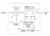
図1は、本実施形態に係る受信システムの構成例を示すブロック図である。
図1に示される受信システムへ入力される受信信号は、RFフィルタ13で帯域制限された後、周波数変換器1に入力される。そして、周波数変換器1にて基準信号とミキシングされ、IF信号に変換される。
Hereinafter, embodiments according to the present invention will be described with reference to the drawings. In each drawing referred to in the following description, the same parts as those in the other drawings are denoted by the same reference numerals.
(First embodiment)
FIG. 1 is a block diagram illustrating a configuration example of a receiving system according to the present embodiment.
The reception signal input to the reception system shown in FIG. 1 is band-limited by the
変換されたIF信号は可変利得アンプおよび折り返し防止フィルタ2を通り、帯域制限フィルタ3に入力される。この帯域制限フィルタ3の出力は、不要な信号が抑圧されて所望のチャネルのIF信号のみが選択されたものとなる。
帯域制限フィルタ3はNパスフィルタで構成されており、離散系である。これを動作させるためのクロック信号およびその高調波を除去するため、帯域制限フィルタ3から出力される信号は、スムージングフィルタ6を経由する。そして、IFアンプ(リミッティングアンプ)7で増幅され、最後に検波回路8でベースバンド信号に変換される。
The converted IF signal passes through the variable gain amplifier and the
The band limiting filter 3 is composed of an N-pass filter and is a discrete system. In order to remove the clock signal for operating this and its harmonics, the signal output from the band limiting filter 3 passes through the smoothing
ここで、受信システムに入力される基準信号は周波数変換器1に入力され、これと同じ基準信号が分周器4にも同時に入力される点が、本実施形態に係る受信システムの特徴である。そして、このような構成は、後述するように、各信号の周波数の関係を所定の関係となるように選択することで実現されるものである。
分周器4で分周された信号は、帯域制限フィルタ3と、Nパスフィルタ用多相クロック生成部5との双方に供給される。また、Nパスフィルタ用多相クロック生成部5で生成された多相クロックは、帯域制限フィルタ3に供給される。なお、帯域制限フィルタ3およびNパスフィルタ用多相クロック生成部5は、図7〜図10に示される従来の構成と同様であるので、ここでは説明を省略する。
Here, the reference signal input to the reception system is input to the
The signal frequency-divided by the
ここで、破線9で囲まれた各構成はセラミックフィルタを用いていないので、集積化することができる。図2は、図1の受信システムを構成するブロックのうち信号周波数が変化するブロックのみを抜き出したものである。なお、図2においては、周波数に変化のないブロックに関しては表記を省略している。また、検波回路8は信号を復調するブロックであるため、図2では表記を省略している。
Here, since each structure surrounded by the broken line 9 does not use a ceramic filter, it can be integrated. FIG. 2 shows only the blocks whose signal frequency changes among the blocks constituting the receiving system of FIG. In FIG. 2, the notation is omitted for blocks whose frequency does not change. Further, since the
受信信号(周波数f1)は、周波数変換器1において基準信号(周波数f2)とミキシングされて帯域通過IF信号(周波数f3)に変換される。また、基準信号(周波数f2)は分周器4により分周器出力信号(周波数f4)となり、帯域制限フィルタ3に供給される。
また、これと同時に、分周器出力信号(周波数f4)はNパスフィルタ用多相クロック生成部5にも供給される。Nパスフィルタ用多相クロック生成部5ではN相クロックが生成され、生成されたN相クロックは帯域制限フィルタ3に供給される。なお、このN相クロックの周波数もf3と同じ周波数になる。
The received signal (frequency f1) is mixed with the reference signal (frequency f2) in the
At the same time, the frequency divider output signal (frequency f4) is also supplied to the N-pass filter
帯域制限フィルタ3に入力された信号(周波数f3)は、帯域制限された信号として出力される。当然のことながら、この帯域制限された信号の周波数はf3である。
この時、下記の式1、式2、式3が成り立つように、基準信号の周波数f2、帯域通過IF信号の周波数f3、分周器出力信号の周波数f4を選択する。
The signal (frequency f3) input to the band limiting filter 3 is output as a band limited signal. Of course, the frequency of this band-limited signal is f3.
At this time, the frequency f2 of the reference signal, the frequency f3 of the band-pass IF signal, and the frequency f4 of the frequency divider output signal are selected so that the following
具体的には、例えば、周波数変換器1の入出力信号の周波数f1、f2との関係から、式1によって周波数f3が決まる。また、周波数f3と式3とによって、帯域制限フィルタ3(Nパスフィルタ)のサンプリングクロックの周波数f4が決まる。さらに、周波数f2とf3とが式2を満たすように設定されることで、一つのみの基準信号を用いた本実施形態の受信システムが実現可能である。
Specifically, for example, the frequency f3 is determined by
このように、上記式1〜式3に示される所定の関係となるように各信号の周波数を選択することで、周波数変換器1に入力される基準信号と分周器4に入力される基準信号とが一つになり、基準信号を共通化できるようになる。よって、基準信号を生成する発振器をそれぞれ別々に用意する必要がない。
なお、本実施形態においては、基準信号はICの外部より供給されるようになっているが、IC内部に単一の発振器が設けられ、この発振器において基準信号が生成されるようになっていてもよい。この場合、複数の発振器をIC内部で用意することもないので、部品コストや消費電力が少なくて済む。
As described above, the reference signal input to the
In this embodiment, the reference signal is supplied from the outside of the IC. However, a single oscillator is provided inside the IC, and the reference signal is generated in this oscillator. Also good. In this case, since a plurality of oscillators are not prepared inside the IC, the component cost and power consumption can be reduced.
より具体的には、例えば、本実施形態の受信システムの仕様としては、受信信号の周波数f1=50.85MHz、基準信号の周波数f2=50.4MHz、帯域通過IF信号の周波数f3=450kHz、分周器出力信号の周波数f4=3.6MHz、と選択することができる。
また、図1に示されるように、周波数変換器1の前段であってIC(破線9で囲まれる部分)の外部にRFフィルタ13が使用される場合には、所望する通過帯域外の不要な信号はRFフィルタ13で抑圧される。よって、Nパスフィルタが帯域制限フィルタ3として使用される場合でも、さらなるICのチップ面積低減や低消費電力化が可能となる。
More specifically, for example, the specifications of the receiving system of the present embodiment include the frequency f1 of the received signal = 50.85 MHz, the frequency f2 of the reference signal = 50.4 MHz, the frequency f3 of the band-pass IF signal = 450 kHz, the minute The frequency f4 of the peripheral output signal can be selected to be 3.6 MHz.
In addition, as shown in FIG. 1, when the
(第2の実施形態)
図3は、本実施形態に係る受信システムの構成例を示すブロック図である。
基本的な構成は図1に示される構成と同様であるが、帯域制限フィルタを、帯域制限フィルタ3´と帯域制限フィルタ11の2段に分け、これらの間にもう1段の可変利得アンプ10を入れている。また、第1の実施形態と同様に、本実施形態においても、式1、式2、式3の条件を満たすように、各信号の周波数を設定する。
このように可変利得アンプと帯域制限フィルタを多段に組むことで、所望する信号周波数以外の不要な信号を抑圧しながら、所望する信号周波数を増幅させることに、より適した受信IFシステムが構築可能となる。
(Second Embodiment)
FIG. 3 is a block diagram illustrating a configuration example of the receiving system according to the present embodiment.
The basic configuration is the same as the configuration shown in FIG. 1, but the band-limiting filter is divided into two stages, a band-limiting filter 3 ′ and a band-limiting
By combining variable gain amplifiers and band limiting filters in multiple stages in this way, a more suitable reception IF system can be constructed to amplify the desired signal frequency while suppressing unnecessary signals other than the desired signal frequency. It becomes.
なお、図3においては可変利得アンプが2段であり、帯域制限フィルタが2段となっているが、それぞれの段数はこれだけに限られない。式1〜式3の条件を充足すれば、可変利得アンプと帯域制限フィルタの段数は他の段数であってもよい。
本実施形態に係る受信システムによれば、帯域制限フィルタが多段に設けられている場合であっても、従来の受信システムに比べて、小面積、低消費電力、かつ低コストである受信システムが提供できる。
In FIG. 3, the variable gain amplifier has two stages and the band limiting filter has two stages, but the number of stages is not limited to this. If the conditions of
According to the receiving system according to the present embodiment, even when the band limiting filters are provided in multiple stages, the receiving system has a smaller area, lower power consumption, and lower cost than the conventional receiving system. Can be provided.
(第3の実施形態)
図4は、本実施形態に係る受信システムの構成例を示すブロック図である。
図1に示される第1の実施形態に係る受信システムのように、周波数変換器1の前段にRFフィルタ13を使用する場合には、所望する通過帯域外の不要な信号はRFフィルタ13で抑圧される。しかし、本実施形態においては、Nパスフィルタ3の前段にプレフィルタ12が設けられている。これにより、レプリカBPF(R−BPF)を抑圧することができる。
(Third embodiment)
FIG. 4 is a block diagram illustrating a configuration example of the receiving system according to the present embodiment.
When the
1 周波数変換器
2 可変利得アンプおよび折り返し防止フィルタ
3 帯域制限フィルタ(Nパスフィルタ)
4 分周器
5 Nパスフィルタ用多相クロック生成部
6 スムージングフィルタ
7 IFアンプ
8 検波回路
10 可変利得アンプ
11 帯域制限フィルタ(Nパスフィルタ)
12 プレフィルタ
13 RFフィルタ
21 周波数変換器
22 帯域制限フィルタ
23 IFアンプ
24 検波回路
25 発振器
31 RFフィルタ
32 RFアンプ
33 イメージリジェクションミキサ
341 発振器
342 発振器
35 ポリフェーズフィルタ
36 折り返し防止フィルタ
37 帯域制限フィルタ(Nパスフィルタ)
381 分周器
382 Nパスフィルタ用多層クロック生成部
39 スムージングフィルタ
40 IFアンプ
41 検波回路
51〜55、60〜64 スイッチ
DESCRIPTION OF
4 Frequency Divider 5 N-phase Filter Multiphase
12 Pre-filter 13
381 Frequency divider 382 N-pass filter
Claims (6)
前記周波数変換された信号である中間周波数信号に対しチャネル選択するためのNパスフィルタで構成された帯域制限フィルタと、
前記Nパスフィルタに供給される動作クロックを生成する分周器と、
前記動作クロックに基づいて、前記Nパスフィルタに供給される多相クロックを生成する多相クロック生成部と、
を有する受信システムであって、
前記分周器は、前記周波数変換器に入力される前記基準信号と同一の周波数の信号の入力を受け付け、この入力された信号に基づいて前記動作クロックを生成することを特徴とする受信システム。 A frequency converter that converts the received signal to an intermediate frequency based on the reference signal;
A band limiting filter composed of an N-pass filter for selecting a channel for the intermediate frequency signal which is the frequency converted signal;
A frequency divider for generating an operation clock supplied to the N-pass filter;
A multi-phase clock generator for generating a multi-phase clock supplied to the N-pass filter based on the operation clock;
A receiving system comprising:
The frequency divider receives an input of a signal having the same frequency as the reference signal input to the frequency converter, and generates the operation clock based on the input signal.
前記基準信号は前記ICチップの外部から供給されることを特徴とする請求項1から3のいずれか一項に記載の受信システム。 The frequency converter, the band limiting filter, the frequency divider, and the multiphase clock generator are formed on the same IC (Integrated Circuit) chip,
The receiving system according to claim 1, wherein the reference signal is supplied from the outside of the IC chip.
Priority Applications (1)
| Application Number | Priority Date | Filing Date | Title |
|---|---|---|---|
| JP2011005498A JP5545875B2 (en) | 2011-01-14 | 2011-01-14 | Receiving system |
Applications Claiming Priority (1)
| Application Number | Priority Date | Filing Date | Title |
|---|---|---|---|
| JP2011005498A JP5545875B2 (en) | 2011-01-14 | 2011-01-14 | Receiving system |
Publications (2)
| Publication Number | Publication Date |
|---|---|
| JP2012147345A true JP2012147345A (en) | 2012-08-02 |
| JP5545875B2 JP5545875B2 (en) | 2014-07-09 |
Family
ID=46790432
Family Applications (1)
| Application Number | Title | Priority Date | Filing Date |
|---|---|---|---|
| JP2011005498A Active JP5545875B2 (en) | 2011-01-14 | 2011-01-14 | Receiving system |
Country Status (1)
| Country | Link |
|---|---|
| JP (1) | JP5545875B2 (en) |
Citations (3)
| Publication number | Priority date | Publication date | Assignee | Title |
|---|---|---|---|---|
| JPH0456524A (en) * | 1990-06-26 | 1992-02-24 | Hitachi Ltd | Tuner circuit |
| JPH0537406A (en) * | 1990-11-28 | 1993-02-12 | Hitachi Ltd | China Circuit |
| JP2006324795A (en) * | 2005-05-17 | 2006-11-30 | Matsushita Electric Ind Co Ltd | Reception IF system having an image rejection mixer and a bandpass filter |
-
2011
- 2011-01-14 JP JP2011005498A patent/JP5545875B2/en active Active
Patent Citations (3)
| Publication number | Priority date | Publication date | Assignee | Title |
|---|---|---|---|---|
| JPH0456524A (en) * | 1990-06-26 | 1992-02-24 | Hitachi Ltd | Tuner circuit |
| JPH0537406A (en) * | 1990-11-28 | 1993-02-12 | Hitachi Ltd | China Circuit |
| JP2006324795A (en) * | 2005-05-17 | 2006-11-30 | Matsushita Electric Ind Co Ltd | Reception IF system having an image rejection mixer and a bandpass filter |
Also Published As
| Publication number | Publication date |
|---|---|
| JP5545875B2 (en) | 2014-07-09 |
Similar Documents
| Publication | Publication Date | Title |
|---|---|---|
| JP3510794B2 (en) | Signal processing device and communication device | |
| JP5974656B2 (en) | Receiver | |
| CN102291126B (en) | Suppression of low-frequency noise from phase detector in phase control loop | |
| US9641316B2 (en) | Frequency divider and radio communications device | |
| JP5284131B2 (en) | Phase synchronization circuit and receiver using the same | |
| Byun et al. | A low-power CMOS Bluetooth RF transceiver with a digital offset canceling DLL-based GFSK demodulator | |
| JP2010268135A (en) | Filter circuit and communication device | |
| CN101123697A (en) | Multi-band television tuner and associated method | |
| JP2017229024A (en) | Phase digital converter, wireless communication device, and wireless communication method | |
| JP2007043290A (en) | Multiplier and wireless communication apparatus using the same | |
| JP2006217563A (en) | Latch circuit, four-phase clock generator and receiver circuit | |
| JP5007891B2 (en) | Clock signal generation method and apparatus for quadrature sampling | |
| EP3228010A1 (en) | Multi-stage frequency dividers and poly-phase signal generators | |
| JPWO2012002026A1 (en) | Frequency converter and receiver using the same | |
| US20090124221A1 (en) | Dual band receiver | |
| JP5694372B2 (en) | Signal decimation technique | |
| JP2017069824A (en) | Receiver and communication system | |
| JP2009153009A (en) | Clock generation circuit | |
| EP2391000B1 (en) | Digital Signal Generator | |
| JP5545875B2 (en) | Receiving system | |
| US8280340B2 (en) | Clock generation for integrated radio frequency receivers | |
| JP2006324795A (en) | Reception IF system having an image rejection mixer and a bandpass filter | |
| JP5015833B2 (en) | CIC filter, filter system, and satellite signal receiving circuit | |
| JP4076558B2 (en) | AM / FM radio receiver and local oscillation circuit used therefor | |
| EP2789105B1 (en) | Heterodyne receiver structure, multi chip module, multi integrated circuit module, and method for processing a radio frequency signal |
Legal Events
| Date | Code | Title | Description |
|---|---|---|---|
| A621 | Written request for application examination |
Free format text: JAPANESE INTERMEDIATE CODE: A621 Effective date: 20130711 |
|
| A977 | Report on retrieval |
Free format text: JAPANESE INTERMEDIATE CODE: A971007 Effective date: 20140218 |
|
| A131 | Notification of reasons for refusal |
Free format text: JAPANESE INTERMEDIATE CODE: A131 Effective date: 20140225 |
|
| A521 | Written amendment |
Free format text: JAPANESE INTERMEDIATE CODE: A523 Effective date: 20140401 |
|
| TRDD | Decision of grant or rejection written | ||
| A01 | Written decision to grant a patent or to grant a registration (utility model) |
Free format text: JAPANESE INTERMEDIATE CODE: A01 Effective date: 20140507 |
|
| A61 | First payment of annual fees (during grant procedure) |
Free format text: JAPANESE INTERMEDIATE CODE: A61 Effective date: 20140509 |
|
| R150 | Certificate of patent or registration of utility model |
Ref document number: 5545875 Country of ref document: JP Free format text: JAPANESE INTERMEDIATE CODE: R150 |
|
| S531 | Written request for registration of change of domicile |
Free format text: JAPANESE INTERMEDIATE CODE: R313531 |
|
| R350 | Written notification of registration of transfer |
Free format text: JAPANESE INTERMEDIATE CODE: R350 |