JP2012169455A - 半導体装置 - Google Patents
半導体装置 Download PDFInfo
- Publication number
- JP2012169455A JP2012169455A JP2011029122A JP2011029122A JP2012169455A JP 2012169455 A JP2012169455 A JP 2012169455A JP 2011029122 A JP2011029122 A JP 2011029122A JP 2011029122 A JP2011029122 A JP 2011029122A JP 2012169455 A JP2012169455 A JP 2012169455A
- Authority
- JP
- Japan
- Prior art keywords
- electrode
- semiconductor device
- thickness
- film
- outer peripheral
- Prior art date
- Legal status (The legal status is an assumption and is not a legal conclusion. Google has not performed a legal analysis and makes no representation as to the accuracy of the status listed.)
- Granted
Links
Images


Landscapes
- Internal Circuitry In Semiconductor Integrated Circuit Devices (AREA)
Abstract
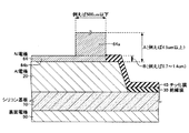
【解決手段】半導体基板10の素子形成面上に第1の金属からなる第1電極20が形成され、該第1電極上に前記第1の金属よりヤング率が大きい第2の金属からなる第2電極64が形成された半導体装置において、
前記第2電極の外周部領域64aの厚さAが、該外周部以外の領域64bの厚さBよりも厚いことを特徴とする。
【選択図】図2
Description
前記第2電極の外周部領域の厚さが、該外周部領域以外の領域の厚さよりも厚いことを特徴とする。
20 Al電極
30 絶縁膜
40 チッ化膜
50 裏面電極
60 上部電極
61 Ti膜
62 Ni膜
63 Au膜
64、65、66 Ni電極
64a、65a、66a 外周領域
64b、65b、66b 中央側領域
66c 外側端面
70 はんだ
80 金属部材
Claims (1)
- 半導体基板の素子形成面上に第1の金属からなる第1電極が形成され、該第1電極上に前記第1の金属よりヤング率が大きい第2の金属からなる第2電極が形成された半導体装置において、
前記第2電極の外周部領域の厚さが、該外周部領域以外の領域の厚さよりも厚いことを特徴とする半導体装置。
Priority Applications (1)
| Application Number | Priority Date | Filing Date | Title |
|---|---|---|---|
| JP2011029122A JP5720287B2 (ja) | 2011-02-14 | 2011-02-14 | 半導体装置 |
Applications Claiming Priority (1)
| Application Number | Priority Date | Filing Date | Title |
|---|---|---|---|
| JP2011029122A JP5720287B2 (ja) | 2011-02-14 | 2011-02-14 | 半導体装置 |
Publications (2)
| Publication Number | Publication Date |
|---|---|
| JP2012169455A true JP2012169455A (ja) | 2012-09-06 |
| JP5720287B2 JP5720287B2 (ja) | 2015-05-20 |
Family
ID=46973334
Family Applications (1)
| Application Number | Title | Priority Date | Filing Date |
|---|---|---|---|
| JP2011029122A Expired - Fee Related JP5720287B2 (ja) | 2011-02-14 | 2011-02-14 | 半導体装置 |
Country Status (1)
| Country | Link |
|---|---|
| JP (1) | JP5720287B2 (ja) |
Cited By (1)
| Publication number | Priority date | Publication date | Assignee | Title |
|---|---|---|---|---|
| JP2018129390A (ja) * | 2017-02-08 | 2018-08-16 | トヨタ自動車株式会社 | 半導体装置 |
Citations (4)
| Publication number | Priority date | Publication date | Assignee | Title |
|---|---|---|---|---|
| JPH06177134A (ja) * | 1992-12-04 | 1994-06-24 | Sony Corp | 電子部品のバンプ構造 |
| JP2001015539A (ja) * | 1999-07-02 | 2001-01-19 | Fujitsu Ltd | 半導体装置及び半導体装置の製造方法 |
| JP2006041011A (ja) * | 2004-07-23 | 2006-02-09 | Optrex Corp | Icチップおよび表示装置 |
| JP2009032949A (ja) * | 2007-07-27 | 2009-02-12 | Sony Chemical & Information Device Corp | Icチップ及びicチップの実装方法 |
-
2011
- 2011-02-14 JP JP2011029122A patent/JP5720287B2/ja not_active Expired - Fee Related
Patent Citations (4)
| Publication number | Priority date | Publication date | Assignee | Title |
|---|---|---|---|---|
| JPH06177134A (ja) * | 1992-12-04 | 1994-06-24 | Sony Corp | 電子部品のバンプ構造 |
| JP2001015539A (ja) * | 1999-07-02 | 2001-01-19 | Fujitsu Ltd | 半導体装置及び半導体装置の製造方法 |
| JP2006041011A (ja) * | 2004-07-23 | 2006-02-09 | Optrex Corp | Icチップおよび表示装置 |
| JP2009032949A (ja) * | 2007-07-27 | 2009-02-12 | Sony Chemical & Information Device Corp | Icチップ及びicチップの実装方法 |
Cited By (1)
| Publication number | Priority date | Publication date | Assignee | Title |
|---|---|---|---|---|
| JP2018129390A (ja) * | 2017-02-08 | 2018-08-16 | トヨタ自動車株式会社 | 半導体装置 |
Also Published As
| Publication number | Publication date |
|---|---|
| JP5720287B2 (ja) | 2015-05-20 |
Similar Documents
| Publication | Publication Date | Title |
|---|---|---|
| JP6249933B2 (ja) | 半導体素子、半導体装置および半導体素子の製造方法 | |
| JP6264230B2 (ja) | 半導体装置 | |
| JP6406975B2 (ja) | 半導体素子および半導体装置 | |
| JP3661695B2 (ja) | 半導体装置 | |
| JP4049035B2 (ja) | 半導体装置の製造方法 | |
| JP6535509B2 (ja) | 半導体装置 | |
| JP7413485B2 (ja) | 半導体装置 | |
| JP3767585B2 (ja) | 半導体装置 | |
| JP2019016738A (ja) | 半導体装置 | |
| JP6607105B2 (ja) | 回路基板及び半導体モジュール、回路基板の製造方法 | |
| JP2005311284A (ja) | パワー半導体素子およびこれを用いた半導体装置 | |
| JP2010003796A (ja) | 半導体装置及びその製造方法 | |
| JP4322189B2 (ja) | 半導体装置 | |
| JP5720287B2 (ja) | 半導体装置 | |
| JP6225414B2 (ja) | 半導体装置 | |
| JP6607771B2 (ja) | 半導体装置 | |
| JP6128005B2 (ja) | 半導体装置 | |
| JP2018085421A (ja) | 半導体装置 | |
| CN112335025A (zh) | 半导体装置 | |
| JP5418654B2 (ja) | 半導体装置 | |
| JP2016134547A (ja) | 半導体装置 | |
| JP4498966B2 (ja) | 金属−セラミックス接合基板 | |
| JP2006261415A (ja) | 半導体装置の製造方法 | |
| JP6558969B2 (ja) | 半導体チップ、半導体装置およびそれらの製造方法 | |
| JP2005268374A (ja) | 半導体素子とその製造方法、及び半導体装置 |
Legal Events
| Date | Code | Title | Description |
|---|---|---|---|
| A621 | Written request for application examination |
Free format text: JAPANESE INTERMEDIATE CODE: A621 Effective date: 20131022 |
|
| A977 | Report on retrieval |
Free format text: JAPANESE INTERMEDIATE CODE: A971007 Effective date: 20140221 |
|
| A131 | Notification of reasons for refusal |
Free format text: JAPANESE INTERMEDIATE CODE: A131 Effective date: 20140311 |
|
| A521 | Request for written amendment filed |
Free format text: JAPANESE INTERMEDIATE CODE: A523 Effective date: 20140508 |
|
| A131 | Notification of reasons for refusal |
Free format text: JAPANESE INTERMEDIATE CODE: A131 Effective date: 20141007 |
|
| A521 | Request for written amendment filed |
Free format text: JAPANESE INTERMEDIATE CODE: A523 Effective date: 20141205 |
|
| TRDD | Decision of grant or rejection written | ||
| A01 | Written decision to grant a patent or to grant a registration (utility model) |
Free format text: JAPANESE INTERMEDIATE CODE: A01 Effective date: 20150224 |
|
| A61 | First payment of annual fees (during grant procedure) |
Free format text: JAPANESE INTERMEDIATE CODE: A61 Effective date: 20150309 |
|
| R151 | Written notification of patent or utility model registration |
Ref document number: 5720287 Country of ref document: JP Free format text: JAPANESE INTERMEDIATE CODE: R151 |
|
| S111 | Request for change of ownership or part of ownership |
Free format text: JAPANESE INTERMEDIATE CODE: R313113 |
|
| R350 | Written notification of registration of transfer |
Free format text: JAPANESE INTERMEDIATE CODE: R350 |
|
| R250 | Receipt of annual fees |
Free format text: JAPANESE INTERMEDIATE CODE: R250 |
|
| R250 | Receipt of annual fees |
Free format text: JAPANESE INTERMEDIATE CODE: R250 |
|
| LAPS | Cancellation because of no payment of annual fees |