JP2012208408A - 表示装置および電子機器 - Google Patents
表示装置および電子機器 Download PDFInfo
- Publication number
- JP2012208408A JP2012208408A JP2011075472A JP2011075472A JP2012208408A JP 2012208408 A JP2012208408 A JP 2012208408A JP 2011075472 A JP2011075472 A JP 2011075472A JP 2011075472 A JP2011075472 A JP 2011075472A JP 2012208408 A JP2012208408 A JP 2012208408A
- Authority
- JP
- Japan
- Prior art keywords
- scattering
- light
- film
- display device
- films
- Prior art date
- Legal status (The legal status is an assumption and is not a legal conclusion. Google has not performed a legal analysis and makes no representation as to the accuracy of the status listed.)
- Granted
Links
Images


Classifications
-
- G—PHYSICS
- G02—OPTICS
- G02F—OPTICAL DEVICES OR ARRANGEMENTS FOR THE CONTROL OF LIGHT BY MODIFICATION OF THE OPTICAL PROPERTIES OF THE MEDIA OF THE ELEMENTS INVOLVED THEREIN; NON-LINEAR OPTICS; FREQUENCY-CHANGING OF LIGHT; OPTICAL LOGIC ELEMENTS; OPTICAL ANALOGUE/DIGITAL CONVERTERS
- G02F1/00—Devices or arrangements for the control of the intensity, colour, phase, polarisation or direction of light arriving from an independent light source, e.g. switching, gating or modulating; Non-linear optics
- G02F1/01—Devices or arrangements for the control of the intensity, colour, phase, polarisation or direction of light arriving from an independent light source, e.g. switching, gating or modulating; Non-linear optics for the control of the intensity, phase, polarisation or colour
- G02F1/13—Devices or arrangements for the control of the intensity, colour, phase, polarisation or direction of light arriving from an independent light source, e.g. switching, gating or modulating; Non-linear optics for the control of the intensity, phase, polarisation or colour based on liquid crystals, e.g. single liquid crystal display cells
- G02F1/133—Constructional arrangements; Operation of liquid crystal cells; Circuit arrangements
- G02F1/1333—Constructional arrangements; Manufacturing methods
- G02F1/1335—Structural association of cells with optical devices, e.g. polarisers or reflectors
- G02F1/133553—Reflecting elements
-
- G—PHYSICS
- G02—OPTICS
- G02F—OPTICAL DEVICES OR ARRANGEMENTS FOR THE CONTROL OF LIGHT BY MODIFICATION OF THE OPTICAL PROPERTIES OF THE MEDIA OF THE ELEMENTS INVOLVED THEREIN; NON-LINEAR OPTICS; FREQUENCY-CHANGING OF LIGHT; OPTICAL LOGIC ELEMENTS; OPTICAL ANALOGUE/DIGITAL CONVERTERS
- G02F1/00—Devices or arrangements for the control of the intensity, colour, phase, polarisation or direction of light arriving from an independent light source, e.g. switching, gating or modulating; Non-linear optics
- G02F1/01—Devices or arrangements for the control of the intensity, colour, phase, polarisation or direction of light arriving from an independent light source, e.g. switching, gating or modulating; Non-linear optics for the control of the intensity, phase, polarisation or colour
- G02F1/13—Devices or arrangements for the control of the intensity, colour, phase, polarisation or direction of light arriving from an independent light source, e.g. switching, gating or modulating; Non-linear optics for the control of the intensity, phase, polarisation or colour based on liquid crystals, e.g. single liquid crystal display cells
- G02F1/133—Constructional arrangements; Operation of liquid crystal cells; Circuit arrangements
- G02F1/1333—Constructional arrangements; Manufacturing methods
- G02F1/1335—Structural association of cells with optical devices, e.g. polarisers or reflectors
-
- G—PHYSICS
- G02—OPTICS
- G02B—OPTICAL ELEMENTS, SYSTEMS OR APPARATUS
- G02B5/00—Optical elements other than lenses
- G02B5/02—Diffusing elements; Afocal elements
- G02B5/0205—Diffusing elements; Afocal elements characterised by the diffusing properties
- G02B5/0257—Diffusing elements; Afocal elements characterised by the diffusing properties creating an anisotropic diffusion characteristic, i.e. distributing output differently in two perpendicular axes
-
- G—PHYSICS
- G02—OPTICS
- G02B—OPTICAL ELEMENTS, SYSTEMS OR APPARATUS
- G02B5/00—Optical elements other than lenses
- G02B5/02—Diffusing elements; Afocal elements
- G02B5/0273—Diffusing elements; Afocal elements characterized by the use
- G02B5/0278—Diffusing elements; Afocal elements characterized by the use used in transmission
-
- G—PHYSICS
- G02—OPTICS
- G02B—OPTICAL ELEMENTS, SYSTEMS OR APPARATUS
- G02B6/00—Light guides; Structural details of arrangements comprising light guides and other optical elements, e.g. couplings
- G02B6/0001—Light guides; Structural details of arrangements comprising light guides and other optical elements, e.g. couplings specially adapted for lighting devices or systems
- G02B6/0011—Light guides; Structural details of arrangements comprising light guides and other optical elements, e.g. couplings specially adapted for lighting devices or systems the light guides being planar or of plate-like form
- G02B6/0033—Means for improving the coupling-out of light from the light guide
- G02B6/005—Means for improving the coupling-out of light from the light guide provided by one optical element, or plurality thereof, placed on the light output side of the light guide
- G02B6/0051—Diffusing sheet or layer
-
- G—PHYSICS
- G02—OPTICS
- G02F—OPTICAL DEVICES OR ARRANGEMENTS FOR THE CONTROL OF LIGHT BY MODIFICATION OF THE OPTICAL PROPERTIES OF THE MEDIA OF THE ELEMENTS INVOLVED THEREIN; NON-LINEAR OPTICS; FREQUENCY-CHANGING OF LIGHT; OPTICAL LOGIC ELEMENTS; OPTICAL ANALOGUE/DIGITAL CONVERTERS
- G02F1/00—Devices or arrangements for the control of the intensity, colour, phase, polarisation or direction of light arriving from an independent light source, e.g. switching, gating or modulating; Non-linear optics
- G02F1/01—Devices or arrangements for the control of the intensity, colour, phase, polarisation or direction of light arriving from an independent light source, e.g. switching, gating or modulating; Non-linear optics for the control of the intensity, phase, polarisation or colour
- G02F1/13—Devices or arrangements for the control of the intensity, colour, phase, polarisation or direction of light arriving from an independent light source, e.g. switching, gating or modulating; Non-linear optics for the control of the intensity, phase, polarisation or colour based on liquid crystals, e.g. single liquid crystal display cells
- G02F1/133—Constructional arrangements; Operation of liquid crystal cells; Circuit arrangements
- G02F1/1333—Constructional arrangements; Manufacturing methods
- G02F1/1335—Structural association of cells with optical devices, e.g. polarisers or reflectors
- G02F1/133504—Diffusing, scattering, diffracting elements
-
- G—PHYSICS
- G02—OPTICS
- G02B—OPTICAL ELEMENTS, SYSTEMS OR APPARATUS
- G02B2207/00—Coding scheme for general features or characteristics of optical elements and systems of subclass G02B, but not including elements and systems which would be classified in G02B6/00 and subgroups
- G02B2207/123—Optical louvre elements, e.g. for directional light blocking
Landscapes
- Physics & Mathematics (AREA)
- Nonlinear Science (AREA)
- General Physics & Mathematics (AREA)
- Optics & Photonics (AREA)
- Mathematical Physics (AREA)
- Chemical & Material Sciences (AREA)
- Crystallography & Structural Chemistry (AREA)
- Liquid Crystal (AREA)
- Optical Elements Other Than Lenses (AREA)
- Devices For Indicating Variable Information By Combining Individual Elements (AREA)
Abstract
【解決手段】反射型の液晶表示パネル10上に、2枚の前方散乱フィルム21,22を含む光学積層体20が設けられている。前方散乱フィルム21,22は、光学積層体20との関係で映像表示面側の特定方向から光が入射してきた場合に、その入射光をほとんど散乱せずに透過させ、液晶表示パネル10で反射され戻ってきた光を大きく散乱するようになっている。さらに、前方散乱フィルム21,22の散乱中心軸方向の透過率が互いに異なっている。
【選択図】図1
Description
1.実施の形態(表示装置)
散乱中心軸方向の透過率が互いに異なる例
2.適用例(電子機器)
上記実施の形態に係る表示装置が電子機器に利用されている例
[構成]
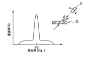
図1は、一実施の形態に係る表示装置1の上面構成の一例を表すものである。なお、図1は模式的に表したものであり、実際の寸法、形状と同一とは限らない。表示装置1は、例えば、図1に示したように、液晶表示パネル10と、液晶表示パネル10上に配置された光学積層体20と、映像信号に応じて表示パネル10を駆動する駆動回路30とを備えている。
液晶表示パネル10は、例えば、図1に示したように、所定の間隙を介して互いに対向するTFT(Thin Film Transistor)基板11および対向基板12と、TFT基板11と対向基板12との間に設けられた液晶層13とを備えている。
光学積層体20は、例えば、図1に示したように、前方散乱フィルム21、前方散乱フィルム22、λ/4板23、λ/2板24および偏光板25を液晶表示パネル10側から順に有している。なお、光学積層体20と液晶表示パネル10とは、例えば、互いに粘着剤や接着剤で貼り合わされている。同様に、光学積層体20内で互いに隣り合う部材同士が、例えば、互いに粘着剤や接着剤で貼り合わされている。
次に、本実施の形態の表示装置1の作用、効果について説明する。
(第1変形例)
上記実施の形態では、前方散乱フィルム22の散乱中心軸AX方向の透過率が、前方散乱フィルム21の散乱中心軸AX方向の透過率よりも相対的に高くなっている場合が例示されていた。しかし、前方散乱フィルム21の散乱中心軸AX方向の透過率が、前方散乱フィルム22の散乱中心軸AX方向の透過率よりも相対的に高くなっていてもよい。このようにした場合であっても、外光L1が前方散乱フィルム22を透過し、反射層14にまで到達する光量が多くなる。その結果、反射層14で反射された光L2のうち前方散乱フィルム21,22で拡散され、正面方向に出射される光の光量も多くなるので、白表示で高輝度を得ることができる。
上記実施の形態では、2枚の前方散乱フィルム21,22が光学積層体20内に設けられていたが、3枚以上の前方散乱フィルムが光学積層体20内に設けられていてもよい。ただし、この場合には、3枚以上の前方散乱フィルムのうち少なくとも2枚の前方散乱フィルムにおいて、一方の前方散乱フィルムの散乱中心軸方向の透過率が、他方の前方散乱フィルムの散乱中心軸方向の透過率よりも相対的に高くなっていればよい。
上記実施の形態では、前方散乱フィルム21,22は、光学積層体20との関係で偏光板25側の特定方向から光が入射してきた場合に、その入射光をほとんど散乱せずに透過させ、反射層14で反射され戻ってきた光を大きく散乱するようになっていた。しかし、前方散乱フィルム21,22は、光学積層体20との関係で偏光板25側の特定方向から光が入射してきた場合に、その入射光を大きく散乱させ、反射層14で反射され戻ってきた光をほとんど散乱せずに透過させるようになっていてもよい。
上記実施の形態では、λ/4板23と偏光板25との間にλ/2板24が設けられていたが、必要に応じて省略することも可能である。また、上記実施の形態において、何らかの層が、必要に応じて、光学積層体20内にさらに設けられていてもよい。
次に、上記実施の形態およびその変形例に係る表示装置1の一適用例について説明する。図17は、本適用例に係る電子機器100の概略構成の一例を表す斜視図である。電子機器100は、携帯電話機であり、例えば、図17に示したように、本体部111と、本体部111に対して開閉可能に設けられた表示体部112とを備えている。本体部111は、操作ボタン115と、送話部116を有している。表示体部112は、表示装置113と、受話部117とを有している。表示装置113は、電話通信に関する各種表示を、表示装置113の表示画面114に表示するようになっている。電子機器100は、表示装置113の動作を制御するための制御部(図示せず)を備えている。この制御部は、電子機器100全体の制御を司る制御部の一部として、またはその制御部とは別に、本体部111または表示体部112の内部に設けられている。
Claims (6)
- 反射型の表示パネルと、
前記表示パネル上に配置された光学積層体と
を備え、
前記光学積層体は、2枚以上の異方性散乱フィルムを有し、
前記複数の異方性散乱フィルムのうち少なくとも2枚のフィルムの散乱中心軸方向の透過率が互いに異なる
表示装置。 - 前記光学積層体に含まれる異方性散乱フィルムのうち散乱中心軸方向の透過率が相対的に高い第1フィルムは、前記光学積層体に含まれる異方性散乱フィルムのうち散乱中心軸方向の透過率が相対的に低い第2フィルムよりも薄くなっている
請求項1に記載の表示装置。 - 前記光学積層体に含まれる異方性散乱フィルムのうち散乱中心軸方向の透過率が相対的に高い第1フィルムは、前記光学積層体に含まれる異方性散乱フィルムのうち散乱中心軸方向の透過率が相対的に低い第2フィルムよりも不明瞭な組織構造となっている
請求項1に記載の表示装置。 - 前記異方性散乱フィルムは、前記光学積層体との関係で所定の方向から外光が入射したときにその外光を透過させ、その透過した光のうち前記表示パネルで反射された光を、散乱中心軸を中心として所定の範囲で散乱させる前方散乱フィルムである
請求項1に記載の表示装置。 - 前記異方性散乱フィルムは、前記光学積層体との関係で所定の方向から外光が入射したときにその外光を、散乱中心軸を中心として所定の範囲で散乱させ、その散乱光のうち前記表示パネルで反射された光を透過させる前方散乱フィルムである
請求項1に記載の表示装置。 - 表示装置を備え、
前記表示装置は、
反射型の表示パネルと、
前記表示パネル上に配置された光学積層体と
を有し、
前記光学積層体は、2枚以上の異方性散乱フィルムを有し、
前記複数の異方性散乱フィルムのうち少なくとも2枚のフィルムの散乱中心軸方向の透過率が互いに異なる
電子機器。
Priority Applications (8)
| Application Number | Priority Date | Filing Date | Title |
|---|---|---|---|
| JP2011075472A JP5749960B2 (ja) | 2011-03-30 | 2011-03-30 | 表示装置および電子機器 |
| US13/415,615 US9291851B2 (en) | 2011-03-30 | 2012-03-08 | Display and electronic unit |
| TW101109514A TWI569064B (zh) | 2011-03-30 | 2012-03-20 | 顯示器及電子單元 |
| KR1020120029457A KR101853976B1 (ko) | 2011-03-30 | 2012-03-22 | 표시 장치 및 전자 기기 |
| EP12002043.3A EP2506066A3 (en) | 2011-03-30 | 2012-03-22 | Display and electronic unit |
| CN201610210487.5A CN105717694B (zh) | 2011-03-30 | 2012-03-23 | 显示装置及电子设备 |
| CN201210080790.XA CN102736306B (zh) | 2011-03-30 | 2012-03-23 | 显示装置及电子设备 |
| US14/939,132 US10191322B2 (en) | 2011-03-30 | 2015-11-12 | Display and electronic unit |
Applications Claiming Priority (1)
| Application Number | Priority Date | Filing Date | Title |
|---|---|---|---|
| JP2011075472A JP5749960B2 (ja) | 2011-03-30 | 2011-03-30 | 表示装置および電子機器 |
Publications (2)
| Publication Number | Publication Date |
|---|---|
| JP2012208408A true JP2012208408A (ja) | 2012-10-25 |
| JP5749960B2 JP5749960B2 (ja) | 2015-07-15 |
Family
ID=46061970
Family Applications (1)
| Application Number | Title | Priority Date | Filing Date |
|---|---|---|---|
| JP2011075472A Active JP5749960B2 (ja) | 2011-03-30 | 2011-03-30 | 表示装置および電子機器 |
Country Status (6)
| Country | Link |
|---|---|
| US (2) | US9291851B2 (ja) |
| EP (1) | EP2506066A3 (ja) |
| JP (1) | JP5749960B2 (ja) |
| KR (1) | KR101853976B1 (ja) |
| CN (2) | CN102736306B (ja) |
| TW (1) | TWI569064B (ja) |
Cited By (9)
| Publication number | Priority date | Publication date | Assignee | Title |
|---|---|---|---|---|
| WO2014088086A1 (ja) * | 2012-12-07 | 2014-06-12 | 株式会社巴川製紙所 | 表示装置 |
| JP2014137467A (ja) * | 2013-01-16 | 2014-07-28 | Japan Display Inc | 表示装置 |
| JP2014142502A (ja) * | 2013-01-24 | 2014-08-07 | Japan Display Inc | 反射型液晶表示装置及び電子機器 |
| JP2014203004A (ja) * | 2013-04-08 | 2014-10-27 | 株式会社ジャパンディスプレイ | 表示装置及び電子機器 |
| WO2014178230A1 (ja) | 2013-04-30 | 2014-11-06 | リンテック株式会社 | ディスプレイ用光拡散フィルムおよびそれを用いた反射型表示装置 |
| CN104597536A (zh) * | 2014-12-30 | 2015-05-06 | 深圳市亿思达科技集团有限公司 | 一种散射板及显示装置 |
| JP2015127819A (ja) * | 2015-02-05 | 2015-07-09 | 株式会社巴川製紙所 | 表示装置 |
| US10330967B2 (en) | 2015-12-22 | 2019-06-25 | Japan Display Inc. | Display device and display panel |
| JP2019219532A (ja) * | 2018-06-20 | 2019-12-26 | リンテック株式会社 | 光拡散制御積層体および反射型表示体 |
Families Citing this family (7)
| Publication number | Priority date | Publication date | Assignee | Title |
|---|---|---|---|---|
| JP5730081B2 (ja) * | 2011-03-08 | 2015-06-03 | 株式会社ジャパンディスプレイ | 表示装置 |
| JP2014178454A (ja) | 2013-03-14 | 2014-09-25 | Japan Display Inc | 液晶表示装置及び電子機器 |
| JP2017167403A (ja) * | 2016-03-17 | 2017-09-21 | 株式会社ジャパンディスプレイ | 表示装置 |
| JP6707416B2 (ja) * | 2016-07-29 | 2020-06-10 | 株式会社ジャパンディスプレイ | 表示装置 |
| JP7446738B2 (ja) | 2019-08-20 | 2024-03-11 | リンテック株式会社 | 光拡散制御体および反射型表示体 |
| JP7546354B2 (ja) * | 2019-12-13 | 2024-09-06 | リンテック株式会社 | 光拡散制御部材の製造方法 |
| JP2023148723A (ja) * | 2022-03-30 | 2023-10-13 | リンテック株式会社 | 視野角制御フィルム |
Citations (6)
| Publication number | Priority date | Publication date | Assignee | Title |
|---|---|---|---|---|
| JPH0996705A (ja) * | 1995-09-29 | 1997-04-08 | Dainippon Printing Co Ltd | 光拡散シート及びそれを使用したエッジライト型面光源並びに液晶表示装置 |
| JP2000275408A (ja) * | 1999-03-24 | 2000-10-06 | Toppan Printing Co Ltd | 光散乱シートとそれを用いた液晶表示装置 |
| WO2001038932A1 (fr) * | 1999-11-24 | 2001-05-31 | Citizen Watch Co., Ltd. | Unite d'affichage a cristaux liquides |
| JP2001356339A (ja) * | 2001-04-24 | 2001-12-26 | Matsushita Electric Ind Co Ltd | 反射型液晶表示素子 |
| JP2002214409A (ja) * | 2001-01-16 | 2002-07-31 | Toppan Printing Co Ltd | 光拡散体および液晶表示装置 |
| WO2008053592A1 (fr) * | 2006-10-31 | 2008-05-08 | Tomoegawa Co., Ltd. | Film de diffusion de lumière anisotrope, ainsi que dispositif d'affichage et dispositif d'affichage à cristaux liquides utilisant ce même film |
Family Cites Families (12)
| Publication number | Priority date | Publication date | Assignee | Title |
|---|---|---|---|---|
| JP2807591B2 (ja) * | 1992-03-06 | 1998-10-08 | シャープ株式会社 | ポリマー分散型液晶表示素子及び反射型液晶表示装置 |
| JPH09113893A (ja) | 1995-10-16 | 1997-05-02 | Hitachi Ltd | 反射型液晶表示素子 |
| CN1204067A (zh) * | 1997-06-16 | 1999-01-06 | 松下电器产业株式会社 | 反射型液晶显示元件 |
| JPH11237623A (ja) | 1998-02-20 | 1999-08-31 | Seiko Epson Corp | 液晶装置及び電子機器 |
| US6424395B1 (en) | 1998-04-08 | 2002-07-23 | Toppan Printing Co., Ltd. | Light scattering film and liquid crystal display device |
| JP3702823B2 (ja) * | 2001-08-23 | 2005-10-05 | セイコーエプソン株式会社 | 液晶表示装置および電子機器 |
| JP2003202415A (ja) | 2001-12-28 | 2003-07-18 | Clariant Internatl Ltd | 制御された散乱・透過特性を有する光学フィルムおよびそれを用いた液晶表示装置 |
| US7719646B2 (en) | 2002-11-15 | 2010-05-18 | Sharp Kabushiki Kaisha | Liquid crystal display device |
| JP4135940B2 (ja) | 2004-10-20 | 2008-08-20 | 株式会社巴川製紙所 | 異方性拡散媒体 |
| JP4664260B2 (ja) * | 2005-09-21 | 2011-04-06 | シャープ株式会社 | 表示装置 |
| US7784954B1 (en) * | 2006-07-25 | 2010-08-31 | Fusion Optix, Inc. | Polarization sensitive light homogenizer |
| JP2010044320A (ja) | 2008-08-18 | 2010-02-25 | Daicel Chem Ind Ltd | 光制御フィルム及びこれを用いたバックライト装置 |
-
2011
- 2011-03-30 JP JP2011075472A patent/JP5749960B2/ja active Active
-
2012
- 2012-03-08 US US13/415,615 patent/US9291851B2/en active Active
- 2012-03-20 TW TW101109514A patent/TWI569064B/zh active
- 2012-03-22 EP EP12002043.3A patent/EP2506066A3/en not_active Ceased
- 2012-03-22 KR KR1020120029457A patent/KR101853976B1/ko active Active
- 2012-03-23 CN CN201210080790.XA patent/CN102736306B/zh active Active
- 2012-03-23 CN CN201610210487.5A patent/CN105717694B/zh active Active
-
2015
- 2015-11-12 US US14/939,132 patent/US10191322B2/en active Active
Patent Citations (6)
| Publication number | Priority date | Publication date | Assignee | Title |
|---|---|---|---|---|
| JPH0996705A (ja) * | 1995-09-29 | 1997-04-08 | Dainippon Printing Co Ltd | 光拡散シート及びそれを使用したエッジライト型面光源並びに液晶表示装置 |
| JP2000275408A (ja) * | 1999-03-24 | 2000-10-06 | Toppan Printing Co Ltd | 光散乱シートとそれを用いた液晶表示装置 |
| WO2001038932A1 (fr) * | 1999-11-24 | 2001-05-31 | Citizen Watch Co., Ltd. | Unite d'affichage a cristaux liquides |
| JP2002214409A (ja) * | 2001-01-16 | 2002-07-31 | Toppan Printing Co Ltd | 光拡散体および液晶表示装置 |
| JP2001356339A (ja) * | 2001-04-24 | 2001-12-26 | Matsushita Electric Ind Co Ltd | 反射型液晶表示素子 |
| WO2008053592A1 (fr) * | 2006-10-31 | 2008-05-08 | Tomoegawa Co., Ltd. | Film de diffusion de lumière anisotrope, ainsi que dispositif d'affichage et dispositif d'affichage à cristaux liquides utilisant ce même film |
Cited By (17)
| Publication number | Priority date | Publication date | Assignee | Title |
|---|---|---|---|---|
| JP2014115421A (ja) * | 2012-12-07 | 2014-06-26 | Tomoegawa Paper Co Ltd | 表示装置 |
| US9581738B2 (en) | 2012-12-07 | 2017-02-28 | Tomoegawa Co., Ltd. | Display apparatus |
| WO2014088086A1 (ja) * | 2012-12-07 | 2014-06-12 | 株式会社巴川製紙所 | 表示装置 |
| JP2014137467A (ja) * | 2013-01-16 | 2014-07-28 | Japan Display Inc | 表示装置 |
| JP2014142502A (ja) * | 2013-01-24 | 2014-08-07 | Japan Display Inc | 反射型液晶表示装置及び電子機器 |
| US9335580B2 (en) | 2013-04-08 | 2016-05-10 | Japan Display Inc. | Display device and electronic apparatus |
| JP2014203004A (ja) * | 2013-04-08 | 2014-10-27 | 株式会社ジャパンディスプレイ | 表示装置及び電子機器 |
| US10359664B2 (en) | 2013-04-08 | 2019-07-23 | Japan Display Inc. | Display device and electronic apparatus |
| US9971190B2 (en) | 2013-04-08 | 2018-05-15 | Japan Display Inc. | Display device and electronic apparatus |
| KR20160000454A (ko) | 2013-04-30 | 2016-01-04 | 린텍 가부시키가이샤 | 디스플레이용 광확산 필름 및 그것을 사용한 반사형 표시 장치 |
| US10185063B2 (en) | 2013-04-30 | 2019-01-22 | Lintec Corporation | Optical-diffusion film for display and reflective display device using same |
| WO2014178230A1 (ja) | 2013-04-30 | 2014-11-06 | リンテック株式会社 | ディスプレイ用光拡散フィルムおよびそれを用いた反射型表示装置 |
| CN104597536A (zh) * | 2014-12-30 | 2015-05-06 | 深圳市亿思达科技集团有限公司 | 一种散射板及显示装置 |
| JP2015127819A (ja) * | 2015-02-05 | 2015-07-09 | 株式会社巴川製紙所 | 表示装置 |
| US10330967B2 (en) | 2015-12-22 | 2019-06-25 | Japan Display Inc. | Display device and display panel |
| JP2019219532A (ja) * | 2018-06-20 | 2019-12-26 | リンテック株式会社 | 光拡散制御積層体および反射型表示体 |
| JP7245004B2 (ja) | 2018-06-20 | 2023-03-23 | リンテック株式会社 | 光拡散制御積層体および反射型表示体 |
Also Published As
| Publication number | Publication date |
|---|---|
| TWI569064B (zh) | 2017-02-01 |
| EP2506066A3 (en) | 2013-12-25 |
| CN102736306A (zh) | 2012-10-17 |
| TW201300883A (zh) | 2013-01-01 |
| US10191322B2 (en) | 2019-01-29 |
| CN105717694A (zh) | 2016-06-29 |
| US20120250158A1 (en) | 2012-10-04 |
| JP5749960B2 (ja) | 2015-07-15 |
| EP2506066A2 (en) | 2012-10-03 |
| CN102736306B (zh) | 2016-05-04 |
| KR20120112063A (ko) | 2012-10-11 |
| CN105717694B (zh) | 2019-06-14 |
| KR101853976B1 (ko) | 2018-05-02 |
| US9291851B2 (en) | 2016-03-22 |
| US20160070140A1 (en) | 2016-03-10 |
Similar Documents
| Publication | Publication Date | Title |
|---|---|---|
| JP5749960B2 (ja) | 表示装置および電子機器 | |
| JP5893256B2 (ja) | 表示装置および電子機器 | |
| TWI269914B (en) | Liquid crystal display device | |
| JP3337028B2 (ja) | 液晶装置及び電子機器 | |
| JP5707275B2 (ja) | 表示装置および電子機器 | |
| WO2007138951A1 (ja) | 液晶表示パネルおよび液晶表示装置、並びに液晶表示パネルの製造方法 | |
| US9599854B2 (en) | Liquid crystal display device and electronic apparatus | |
| CN102819154B (zh) | 液晶面板及显示装置 | |
| JP2012155068A (ja) | 表示パネル、表示装置および電子機器 | |
| JP2013047745A (ja) | 表示パネルおよび表示装置 | |
| US20140092347A1 (en) | Liquid crystal display panel and liquid crystal display device | |
| CN110770642B (zh) | 液晶面板 | |
| CN116583781B (zh) | 显示面板及显示装置 | |
| CN108780252A (zh) | 显示装置 | |
| JP4619742B2 (ja) | 液晶表示装置 | |
| US20120140150A1 (en) | Liquid crystal device and electronic apparatus | |
| JP5804501B2 (ja) | 表示パネル、表示装置および電子機器 | |
| WO2011148701A1 (ja) | カラーフィルタおよびこれを備えた反射型表示装置 | |
| JP3337029B2 (ja) | 液晶装置及び電子機器 | |
| CN115826305A (zh) | 一种液晶显示面板及显示装置 | |
| JP2004126107A (ja) | 液晶表示素子 | |
| JP2007047205A (ja) | 光学シート、電界制御型パネル、照明装置、液晶表示装置、および光学シートの製造方法 | |
| JP2009294564A (ja) | 液晶表示素子 |
Legal Events
| Date | Code | Title | Description |
|---|---|---|---|
| RD03 | Notification of appointment of power of attorney |
Free format text: JAPANESE INTERMEDIATE CODE: A7423 Effective date: 20130328 |
|
| A621 | Written request for application examination |
Free format text: JAPANESE INTERMEDIATE CODE: A621 Effective date: 20140110 |
|
| A711 | Notification of change in applicant |
Free format text: JAPANESE INTERMEDIATE CODE: A712 Effective date: 20140110 |
|
| A131 | Notification of reasons for refusal |
Free format text: JAPANESE INTERMEDIATE CODE: A131 Effective date: 20140909 |
|
| A977 | Report on retrieval |
Free format text: JAPANESE INTERMEDIATE CODE: A971007 Effective date: 20140910 |
|
| A521 | Request for written amendment filed |
Free format text: JAPANESE INTERMEDIATE CODE: A523 Effective date: 20141107 |
|
| TRDD | Decision of grant or rejection written | ||
| A01 | Written decision to grant a patent or to grant a registration (utility model) |
Free format text: JAPANESE INTERMEDIATE CODE: A01 Effective date: 20150428 |
|
| A61 | First payment of annual fees (during grant procedure) |
Free format text: JAPANESE INTERMEDIATE CODE: A61 Effective date: 20150515 |
|
| R150 | Certificate of patent or registration of utility model |
Ref document number: 5749960 Country of ref document: JP Free format text: JAPANESE INTERMEDIATE CODE: R150 |
|
| R250 | Receipt of annual fees |
Free format text: JAPANESE INTERMEDIATE CODE: R250 |
|
| R250 | Receipt of annual fees |
Free format text: JAPANESE INTERMEDIATE CODE: R250 |
|
| R250 | Receipt of annual fees |
Free format text: JAPANESE INTERMEDIATE CODE: R250 |
|
| R250 | Receipt of annual fees |
Free format text: JAPANESE INTERMEDIATE CODE: R250 |
|
| R250 | Receipt of annual fees |
Free format text: JAPANESE INTERMEDIATE CODE: R250 |
|
| R250 | Receipt of annual fees |
Free format text: JAPANESE INTERMEDIATE CODE: R250 |
|
| R250 | Receipt of annual fees |
Free format text: JAPANESE INTERMEDIATE CODE: R250 |
|
| R250 | Receipt of annual fees |
Free format text: JAPANESE INTERMEDIATE CODE: R250 |
|
| S111 | Request for change of ownership or part of ownership |
Free format text: JAPANESE INTERMEDIATE CODE: R313113 |
|
| R350 | Written notification of registration of transfer |
Free format text: JAPANESE INTERMEDIATE CODE: R350 |