JP2016524155A - 計測標的の偏光測定及び対応する標的設計 - Google Patents
計測標的の偏光測定及び対応する標的設計 Download PDFInfo
- Publication number
- JP2016524155A JP2016524155A JP2016524217A JP2016524217A JP2016524155A JP 2016524155 A JP2016524155 A JP 2016524155A JP 2016524217 A JP2016524217 A JP 2016524217A JP 2016524217 A JP2016524217 A JP 2016524217A JP 2016524155 A JP2016524155 A JP 2016524155A
- Authority
- JP
- Japan
- Prior art keywords
- target
- target structure
- measurement
- background
- contrast
- Prior art date
- Legal status (The legal status is an assumption and is not a legal conclusion. Google has not performed a legal analysis and makes no representation as to the accuracy of the status listed.)
- Granted
Links
Images


Classifications
-
- G—PHYSICS
- G01—MEASURING; TESTING
- G01B—MEASURING LENGTH, THICKNESS OR SIMILAR LINEAR DIMENSIONS; MEASURING ANGLES; MEASURING AREAS; MEASURING IRREGULARITIES OF SURFACES OR CONTOURS
- G01B11/00—Measuring arrangements characterised by the use of optical techniques
- G01B11/02—Measuring arrangements characterised by the use of optical techniques for measuring length, width or thickness
- G01B11/06—Measuring arrangements characterised by the use of optical techniques for measuring length, width or thickness for measuring thickness ; e.g. of sheet material
-
- G—PHYSICS
- G01—MEASURING; TESTING
- G01B—MEASURING LENGTH, THICKNESS OR SIMILAR LINEAR DIMENSIONS; MEASURING ANGLES; MEASURING AREAS; MEASURING IRREGULARITIES OF SURFACES OR CONTOURS
- G01B11/00—Measuring arrangements characterised by the use of optical techniques
- G01B11/26—Measuring arrangements characterised by the use of optical techniques for measuring angles or tapers; for testing the alignment of axes
- G01B11/27—Measuring arrangements characterised by the use of optical techniques for measuring angles or tapers; for testing the alignment of axes for testing the alignment of axes
- G01B11/272—Measuring arrangements characterised by the use of optical techniques for measuring angles or tapers; for testing the alignment of axes for testing the alignment of axes using photoelectric detection means
-
- G—PHYSICS
- G01—MEASURING; TESTING
- G01N—INVESTIGATING OR ANALYSING MATERIALS BY DETERMINING THEIR CHEMICAL OR PHYSICAL PROPERTIES
- G01N21/00—Investigating or analysing materials by the use of optical means, i.e. using sub-millimetre waves, infrared, visible or ultraviolet light
- G01N21/84—Systems specially adapted for particular applications
- G01N21/88—Investigating the presence of flaws or contamination
- G01N21/95—Investigating the presence of flaws or contamination characterised by the material or shape of the object to be examined
- G01N21/9501—Semiconductor wafers
-
- G—PHYSICS
- G01—MEASURING; TESTING
- G01N—INVESTIGATING OR ANALYSING MATERIALS BY DETERMINING THEIR CHEMICAL OR PHYSICAL PROPERTIES
- G01N21/00—Investigating or analysing materials by the use of optical means, i.e. using sub-millimetre waves, infrared, visible or ultraviolet light
- G01N21/84—Systems specially adapted for particular applications
- G01N21/88—Investigating the presence of flaws or contamination
- G01N21/95—Investigating the presence of flaws or contamination characterised by the material or shape of the object to be examined
- G01N21/956—Inspecting patterns on the surface of objects
-
- G—PHYSICS
- G06—COMPUTING OR CALCULATING; COUNTING
- G06F—ELECTRIC DIGITAL DATA PROCESSING
- G06F30/00—Computer-aided design [CAD]
- G06F30/30—Circuit design
- G06F30/39—Circuit design at the physical level
- G06F30/392—Floor-planning or layout, e.g. partitioning or placement
-
- G—PHYSICS
- G06—COMPUTING OR CALCULATING; COUNTING
- G06F—ELECTRIC DIGITAL DATA PROCESSING
- G06F30/00—Computer-aided design [CAD]
- G06F30/30—Circuit design
- G06F30/39—Circuit design at the physical level
- G06F30/398—Design verification or optimisation, e.g. using design rule check [DRC], layout versus schematics [LVS] or finite element methods [FEM]
-
- G—PHYSICS
- G01—MEASURING; TESTING
- G01B—MEASURING LENGTH, THICKNESS OR SIMILAR LINEAR DIMENSIONS; MEASURING ANGLES; MEASURING AREAS; MEASURING IRREGULARITIES OF SURFACES OR CONTOURS
- G01B2210/00—Aspects not specifically covered by any group under G01B, e.g. of wheel alignment, caliper-like sensors
- G01B2210/56—Measuring geometric parameters of semiconductor structures, e.g. profile, critical dimensions or trench depth
-
- G—PHYSICS
- G01—MEASURING; TESTING
- G01B—MEASURING LENGTH, THICKNESS OR SIMILAR LINEAR DIMENSIONS; MEASURING ANGLES; MEASURING AREAS; MEASURING IRREGULARITIES OF SURFACES OR CONTOURS
- G01B2290/00—Aspects of interferometers not specifically covered by any group under G01B9/02
- G01B2290/70—Using polarization in the interferometer
-
- G—PHYSICS
- G01—MEASURING; TESTING
- G01N—INVESTIGATING OR ANALYSING MATERIALS BY DETERMINING THEIR CHEMICAL OR PHYSICAL PROPERTIES
- G01N21/00—Investigating or analysing materials by the use of optical means, i.e. using sub-millimetre waves, infrared, visible or ultraviolet light
- G01N21/84—Systems specially adapted for particular applications
- G01N21/88—Investigating the presence of flaws or contamination
- G01N21/8806—Specially adapted optical and illumination features
- G01N2021/8848—Polarisation of light
-
- H—ELECTRICITY
- H10—SEMICONDUCTOR DEVICES; ELECTRIC SOLID-STATE DEVICES NOT OTHERWISE PROVIDED FOR
- H10P—GENERIC PROCESSES OR APPARATUS FOR THE MANUFACTURE OR TREATMENT OF DEVICES COVERED BY CLASS H10
- H10P74/00—Testing or measuring during manufacture or treatment of wafers, substrates or devices
- H10P74/27—Structural arrangements therefor
Landscapes
- Physics & Mathematics (AREA)
- General Physics & Mathematics (AREA)
- Engineering & Computer Science (AREA)
- Immunology (AREA)
- Pathology (AREA)
- General Health & Medical Sciences (AREA)
- Biochemistry (AREA)
- Analytical Chemistry (AREA)
- Chemical & Material Sciences (AREA)
- Health & Medical Sciences (AREA)
- Life Sciences & Earth Sciences (AREA)
- Theoretical Computer Science (AREA)
- Computer Hardware Design (AREA)
- General Engineering & Computer Science (AREA)
- Geometry (AREA)
- Evolutionary Computation (AREA)
- Architecture (AREA)
- Length Measuring Devices By Optical Means (AREA)
- Investigating Materials By The Use Of Optical Means Adapted For Particular Applications (AREA)
- Manufacturing & Machinery (AREA)
- Exposure And Positioning Against Photoresist Photosensitive Materials (AREA)
- Testing Or Measuring Of Semiconductors Or The Like (AREA)
- Testing Of Optical Devices Or Fibers (AREA)
Abstract
Description
本願は、2013年6月27日に出願された米国仮特許出願第61/840,339号、及び2013年12月13日に出願された同第61/916,018号の利益を主張するものであり、それらは参照によりその全体が本明細書に組み込まれる。
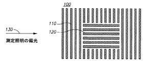
計測標的は、ウエハ製造ステップの質を示し、ウエハ上の構造の設計と実装との間の対応を定量化するパラメータの測定を可能にするように設計される。特定の構造としての計測標的は、デバイスの類似性及び光学測定可能性に対する必要性を最適化する。
Claims (20)
- 標的構造を、偏光下でその背景に対して指定のコントラスト閾値を上回る高コントラストを有する一方で、非偏光下でその背景に対して前記指定のコントラスト閾値を下回る低コントラストを有するように設計するステップを含み、
前記設計するステップは、少なくとも1つのコンピュータプロセッサによって実行される、
ことを特徴とする方法。 - 前記標的構造を、その製造プロセスに対して完全にプロセス適合性となるように設計するステップをさらに含む、
ことを特徴とする請求項1に記載の方法。 - 前記標的構造を、前記標的構造の背景形体に垂直な形体を有するように構成するステップをさらに含む、
ことを特徴とする請求項1に記載の方法。 - 偏光下で前記標的構造の背景に対する前記標的構造のコントラストを維持又は強化するように、前記標的構造の領域内に追加の層を設計するステップをさらに含む、
ことを特徴とする請求項1に記載の方法。 - 前記標的構造を、その背景形体から指定の範囲まで離間させるステップをさらに含む、
ことを特徴とする請求項1に記載の方法。 - 前記設計された標的構造を製造するステップをさらに含む、
ことを特徴とする請求項1〜5のいずれか1項に記載の方法。 - 前記標的構造を偏光下で測定し、前記標的構造を前記標的構造の背景と区別するステップをさらに含む、
ことを特徴とする請求項5に記載の方法。 - 前記標的構造を様々な照明条件下で繰り返し測定するステップと、
複数の測定から追加の測定データを抽出するステップと、
をさらに含むことを特徴とする請求項7に記載の方法。 - 前記標的構造と前記標的構造の背景との間の前記コントラストを強化するように、各層の測定条件を調整するステップをさらに含む、
ことを特徴とする請求項7に記載の方法。 - ゼロ次回析パターンを除去した後に、一次回析パターンを測定するステップをさらに含む、
ことを特徴とする請求項8に記載の方法。 - 前記測定するステップは、連結された偏光子、前記測定の光路内の代替偏光子、干渉計、可変リターダ偏光子、瞳面におけるゼロ次ブロッカ、及び偏光源のうちの少なくとも1つを使用して実行される、
ことを特徴とする請求項7に記載の方法。 - コンピュータ可読プログラムが記憶されたコンピュータ可読記憶媒体を備えるコンピュータプログラム製品であって、
前記コンピュータ可読プログラムは、請求項1〜11のいずれか1項に記載の方法を実行するように構成される、
ことを特徴とするコンピュータプログラム製品。 - 請求項1〜11のいずれか1項に記載の方法に従って設計又は製造されることを特徴とする標的設計ファイル。
- 請求項1〜11のいずれか1項に記載の方法に従って設計、製造、又は測定されることを特徴とする計測標的。
- 標的構造を備える計測標的であって、
前記標的構造が、偏光下でその背景に対して指定のコントラスト閾値を上回る高コントラストを有する一方で、非偏光下でその背景に対して前記指定のコントラスト閾値を下回る低コントラストを有するように配列され、かつそれらの製造プロセスに対して完全にプロセス適合性となるようにさらに配列される、
ことを特徴とする計測標的。 - 前記標的構造は、背景形体に垂直な形体を備える、
ことを特徴とする請求項15に記載の計測標的。 - 偏光下で前記標的構造の背景に対する前記標的構造のコントラストを維持又は強化するように、前記標的構造の領域内に追加の層をさらに備える、
ことを特徴とする請求項15に記載の計測標的。 - 前記標的構造は、その背景形体から指定の範囲まで離間される、
ことを特徴とする請求項15に記載の計測標的。 - 請求項15〜18のいずれか1項に記載の計測標的の計測測定。
- 様々な照明条件下で繰り返し実行される請求項19に記載の計測測定、及び複数の測定から抽出される追加の測定データ。
Applications Claiming Priority (5)
| Application Number | Priority Date | Filing Date | Title |
|---|---|---|---|
| US201361840339P | 2013-06-27 | 2013-06-27 | |
| US61/840,339 | 2013-06-27 | ||
| US201361916018P | 2013-12-13 | 2013-12-13 | |
| US61/916,018 | 2013-12-13 | ||
| PCT/US2014/044440 WO2014210381A1 (en) | 2013-06-27 | 2014-06-26 | Polarization measurements of metrology targets and corresponding target designs |
Related Child Applications (1)
| Application Number | Title | Priority Date | Filing Date |
|---|---|---|---|
| JP2019186136A Division JP6875483B2 (ja) | 2013-06-27 | 2019-10-09 | 計測標的の偏光測定及び対応する標的設計 |
Publications (3)
| Publication Number | Publication Date |
|---|---|
| JP2016524155A true JP2016524155A (ja) | 2016-08-12 |
| JP2016524155A5 JP2016524155A5 (ja) | 2017-08-03 |
| JP6602755B2 JP6602755B2 (ja) | 2019-11-06 |
Family
ID=52142695
Family Applications (2)
| Application Number | Title | Priority Date | Filing Date |
|---|---|---|---|
| JP2016524217A Active JP6602755B2 (ja) | 2013-06-27 | 2014-06-26 | 計測標的の偏光測定及び対応する標的設計 |
| JP2019186136A Active JP6875483B2 (ja) | 2013-06-27 | 2019-10-09 | 計測標的の偏光測定及び対応する標的設計 |
Family Applications After (1)
| Application Number | Title | Priority Date | Filing Date |
|---|---|---|---|
| JP2019186136A Active JP6875483B2 (ja) | 2013-06-27 | 2019-10-09 | 計測標的の偏光測定及び対応する標的設計 |
Country Status (6)
| Country | Link |
|---|---|
| US (2) | US10458777B2 (ja) |
| JP (2) | JP6602755B2 (ja) |
| KR (2) | KR102333504B1 (ja) |
| CN (2) | CN105408721B (ja) |
| TW (1) | TWI675998B (ja) |
| WO (1) | WO2014210381A1 (ja) |
Families Citing this family (13)
| Publication number | Priority date | Publication date | Assignee | Title |
|---|---|---|---|---|
| TWI603216B (zh) * | 2012-11-21 | 2017-10-21 | 克萊譚克公司 | 處理相容分段目標及設計方法 |
| US9851300B1 (en) * | 2014-04-04 | 2017-12-26 | Kla-Tencor Corporation | Decreasing inaccuracy due to non-periodic effects on scatterometric signals |
| US10228320B1 (en) | 2014-08-08 | 2019-03-12 | KLA—Tencor Corporation | Achieving a small pattern placement error in metrology targets |
| KR102574171B1 (ko) * | 2014-08-29 | 2023-09-06 | 에이에스엠엘 네델란즈 비.브이. | 메트롤로지 방법, 타겟 및 기판 |
| JP6789295B2 (ja) * | 2015-12-08 | 2020-11-25 | ケーエルエー コーポレイション | 偏光ターゲットおよび偏光照明を用いた回折光の振幅および位相の制御 |
| US10897566B2 (en) | 2016-09-28 | 2021-01-19 | Kla-Tencor Corporation | Direct focusing with image binning in metrology tools |
| WO2018226215A1 (en) * | 2017-06-06 | 2018-12-13 | Kla-Tencor Corporation | Reticle optimization algorithms and optimal target design |
| US10409948B1 (en) * | 2017-09-29 | 2019-09-10 | Cadence Design Systems, Inc. | Topology preserving schematic transformations for RF net editing |
| US10837919B2 (en) | 2017-11-06 | 2020-11-17 | Kla Corporation | Single cell scatterometry overlay targets |
| WO2021144066A1 (en) * | 2020-01-16 | 2021-07-22 | Asml Netherlands B.V. | Substrate, patterning device and lithographic apparatuses |
| JP2025504941A (ja) * | 2022-01-28 | 2025-02-19 | ディー・ツー・エス・インコーポレイテッド | レチクル強化技術のための方法及びシステム |
| KR102767520B1 (ko) * | 2022-10-12 | 2025-02-14 | (주)힉스컴퍼니 | 디지털 홀로그래픽 현미경을 제어하는 방법 및 장치 |
| US12411420B2 (en) | 2023-09-29 | 2025-09-09 | Kla Corporation | Small in-die target design for overlay measurement |
Citations (7)
| Publication number | Priority date | Publication date | Assignee | Title |
|---|---|---|---|---|
| JP2003247807A (ja) * | 2002-02-25 | 2003-09-05 | Hitachi Ltd | 合わせ精度計測装置及びその方法並びに半導体装置の製造方法及びそのシステム |
| JP2004508711A (ja) * | 2000-08-30 | 2004-03-18 | ケーエルエー−テンカー・コーポレーション | 重ね合わせマーク、重ね合わせマークの設計方法および重ね合わせ測定の方法 |
| US20050012928A1 (en) * | 2003-07-17 | 2005-01-20 | Abdurrahman Sezginer | Apparatus and method for measuring overlay by diffraction gratings |
| JP2006518942A (ja) * | 2003-02-22 | 2006-08-17 | ケーエルエー−テンカー テクノロジィース コーポレイション | 散乱計測を用いてオーバレイ誤差を検出する装置および方法 |
| JP2007096292A (ja) * | 2005-09-01 | 2007-04-12 | Infineon Technologies Ag | 偏光リソグラフィーのためのオーバーレイターゲット |
| JP2009539109A (ja) * | 2006-06-01 | 2009-11-12 | ケーエルエー−テンカー テクノロジィース コーポレイション | 次数選択されたオーバレイ測定 |
| US20120033215A1 (en) * | 2010-08-03 | 2012-02-09 | Kla-Tecor Corporation | Multi-layer overlay metrology target and complimentary overlay metrology measurement systems |
Family Cites Families (30)
| Publication number | Priority date | Publication date | Assignee | Title |
|---|---|---|---|---|
| US6023338A (en) * | 1996-07-12 | 2000-02-08 | Bareket; Noah | Overlay alignment measurement of wafers |
| CN1163737C (zh) * | 2000-03-07 | 2004-08-25 | 中国科学院长春光学精密机械与物理研究所 | 一种综合测量液晶器件参数的装置及方法 |
| US7068833B1 (en) * | 2000-08-30 | 2006-06-27 | Kla-Tencor Corporation | Overlay marks, methods of overlay mark design and methods of overlay measurements |
| US7050162B2 (en) * | 2002-01-16 | 2006-05-23 | Therma-Wave, Inc. | Optical metrology tool having improved contrast |
| JP3695398B2 (ja) * | 2002-01-30 | 2005-09-14 | 富士ゼロックス株式会社 | 光学式エンコーダ及びエンコーダ用スケール |
| SG112969A1 (en) * | 2003-12-22 | 2005-07-28 | Asml Netherlands Bv | Lithographic apparatus and methods for use thereof |
| US20050286052A1 (en) * | 2004-06-23 | 2005-12-29 | Kevin Huggins | Elongated features for improved alignment process integration |
| KR100684872B1 (ko) * | 2004-08-03 | 2007-02-20 | 삼성전자주식회사 | 빛의 편광을 공간적으로 제어하는 광학 시스템 및 이를제작하는 방법 |
| CN1300564C (zh) * | 2004-12-28 | 2007-02-14 | 天津大学 | 基于角度测量的原子力显微镜测量方法 |
| DE102005046973B4 (de) * | 2005-09-30 | 2014-01-30 | Globalfoundries Inc. | Struktur und Verfahren zum gleichzeitigen Bestimmen einer Überlagerungsgenauigkeit und eines Musteranordnungsfehlers |
| US7324193B2 (en) * | 2006-03-30 | 2008-01-29 | Tokyo Electron Limited | Measuring a damaged structure formed on a wafer using optical metrology |
| JP5201350B2 (ja) * | 2006-07-14 | 2013-06-05 | 株式会社ニコン | 表面検査装置 |
| WO2008090853A1 (ja) * | 2007-01-22 | 2008-07-31 | Tokyo University Of Science Educational Foundation Administrative Organization | 回転電気機械 |
| JP4949073B2 (ja) * | 2007-02-23 | 2012-06-06 | 株式会社 日立ディスプレイズ | 液晶表示装置 |
| US8004678B2 (en) * | 2007-06-26 | 2011-08-23 | Intel Corporation | Wafer level alignment structures using subwavelength grating polarizers |
| US8161728B2 (en) * | 2007-06-28 | 2012-04-24 | United Technologies Corp. | Gas turbines with multiple gas flow paths |
| SG153747A1 (en) * | 2007-12-13 | 2009-07-29 | Asml Netherlands Bv | Alignment method, alignment system and product with alignment mark |
| US20090265148A1 (en) * | 2008-04-16 | 2009-10-22 | Synopsys, Inc. | Modeling a sector-polarized-illumination source in an optical lithography system |
| JP5007979B2 (ja) * | 2008-05-22 | 2012-08-22 | 独立行政法人産業技術総合研究所 | 欠陥を検査する方法及び欠陥検査装置 |
| CN101513366B (zh) * | 2009-03-18 | 2011-03-23 | 天津大学 | 基于ps-oct的三维可视化成像方法 |
| NL2004897A (en) * | 2009-06-25 | 2010-12-27 | Asml Netherlands Bv | Producing a marker pattern and measurement of an exposure-related property of an exposure apparatus. |
| TWI423166B (zh) * | 2009-12-04 | 2014-01-11 | Huper Lab Co Ltd | 判斷輸入影像是否為霧化影像之方法、判斷輸入影像的霧級數之方法及霧化影像濾清方法 |
| CN101915556B (zh) * | 2010-07-09 | 2011-11-09 | 浙江大学 | 可用于低反射率光学球面面形检测的偏振点衍射干涉系统 |
| KR101492205B1 (ko) * | 2010-11-12 | 2015-02-10 | 에이에스엠엘 네델란즈 비.브이. | 메트롤로지 방법 및 장치, 리소그래피 시스템, 및 디바이스 제조 방법 |
| US8681413B2 (en) * | 2011-06-27 | 2014-03-25 | Kla-Tencor Corporation | Illumination control |
| CN102332165B (zh) * | 2011-09-15 | 2013-08-21 | 中国科学院长春光学精密机械与物理研究所 | 复杂背景下动目标或弱小目标的实时鲁棒跟踪装置 |
| US9093458B2 (en) * | 2012-09-06 | 2015-07-28 | Kla-Tencor Corporation | Device correlated metrology (DCM) for OVL with embedded SEM structure overlay targets |
| WO2014062972A1 (en) * | 2012-10-18 | 2014-04-24 | Kla-Tencor Corporation | Symmetric target design in scatterometry overlay metrology |
| US20140240705A1 (en) * | 2013-02-27 | 2014-08-28 | Kabushiki Kaisha Toshiba | Semiconductor device, reticle method for checking position misalignment and method for manufacturing position misalignment checking mark |
| KR102285895B1 (ko) * | 2014-03-31 | 2021-08-04 | 케이엘에이 코포레이션 | 산란측정 계측을 이용한 초점 측정 |
-
2014
- 2014-06-26 KR KR1020217014021A patent/KR102333504B1/ko active Active
- 2014-06-26 CN CN201480041321.4A patent/CN105408721B/zh active Active
- 2014-06-26 JP JP2016524217A patent/JP6602755B2/ja active Active
- 2014-06-26 KR KR1020167001849A patent/KR102252341B1/ko active Active
- 2014-06-26 WO PCT/US2014/044440 patent/WO2014210381A1/en not_active Ceased
- 2014-06-26 CN CN201911299611.XA patent/CN111043958B/zh active Active
- 2014-06-27 TW TW103122413A patent/TWI675998B/zh active
-
2015
- 2015-11-23 US US14/949,444 patent/US10458777B2/en active Active
-
2019
- 2019-10-09 JP JP2019186136A patent/JP6875483B2/ja active Active
- 2019-10-28 US US16/665,759 patent/US11060845B2/en active Active
Patent Citations (7)
| Publication number | Priority date | Publication date | Assignee | Title |
|---|---|---|---|---|
| JP2004508711A (ja) * | 2000-08-30 | 2004-03-18 | ケーエルエー−テンカー・コーポレーション | 重ね合わせマーク、重ね合わせマークの設計方法および重ね合わせ測定の方法 |
| JP2003247807A (ja) * | 2002-02-25 | 2003-09-05 | Hitachi Ltd | 合わせ精度計測装置及びその方法並びに半導体装置の製造方法及びそのシステム |
| JP2006518942A (ja) * | 2003-02-22 | 2006-08-17 | ケーエルエー−テンカー テクノロジィース コーポレイション | 散乱計測を用いてオーバレイ誤差を検出する装置および方法 |
| US20050012928A1 (en) * | 2003-07-17 | 2005-01-20 | Abdurrahman Sezginer | Apparatus and method for measuring overlay by diffraction gratings |
| JP2007096292A (ja) * | 2005-09-01 | 2007-04-12 | Infineon Technologies Ag | 偏光リソグラフィーのためのオーバーレイターゲット |
| JP2009539109A (ja) * | 2006-06-01 | 2009-11-12 | ケーエルエー−テンカー テクノロジィース コーポレイション | 次数選択されたオーバレイ測定 |
| US20120033215A1 (en) * | 2010-08-03 | 2012-02-09 | Kla-Tecor Corporation | Multi-layer overlay metrology target and complimentary overlay metrology measurement systems |
Also Published As
| Publication number | Publication date |
|---|---|
| KR20210057833A (ko) | 2021-05-21 |
| WO2014210381A1 (en) | 2014-12-31 |
| US20200158492A1 (en) | 2020-05-21 |
| CN111043958A (zh) | 2020-04-21 |
| US20160178351A1 (en) | 2016-06-23 |
| KR102252341B1 (ko) | 2021-05-18 |
| TWI675998B (zh) | 2019-11-01 |
| KR102333504B1 (ko) | 2021-12-01 |
| US10458777B2 (en) | 2019-10-29 |
| US11060845B2 (en) | 2021-07-13 |
| TW201510469A (zh) | 2015-03-16 |
| CN111043958B (zh) | 2021-11-16 |
| CN105408721B (zh) | 2020-01-10 |
| JP2020074387A (ja) | 2020-05-14 |
| JP6602755B2 (ja) | 2019-11-06 |
| KR20160027017A (ko) | 2016-03-09 |
| CN105408721A (zh) | 2016-03-16 |
| JP6875483B2 (ja) | 2021-05-26 |
Similar Documents
| Publication | Publication Date | Title |
|---|---|---|
| JP6875483B2 (ja) | 計測標的の偏光測定及び対応する標的設計 | |
| JP2016524155A5 (ja) | ||
| KR102590192B1 (ko) | 디바이스 피처에 대해 회전된 각도로 배향된 계측 타겟을 제조하는 시스템 및 방법 | |
| JP6723269B2 (ja) | 焦点感応オーバーレイターゲットを使用する焦点決定のためのシステムおよび方法 | |
| TWI431245B (zh) | 自參考干涉計,對準系統及微影裝置 | |
| TW202536502A (zh) | 計量目標,以及計量系統 | |
| US20240184218A1 (en) | Metrology Apparatus | |
| US9036143B2 (en) | Inspection apparatus and inspection method | |
| TW201003332A (en) | Overlay measurement apparatus, and lithographic apparatus and device manufacturing method using such overlay measurement apparatus | |
| TWI736730B (zh) | 用於焦點敏感式量測目標之系統及方法 | |
| US20120224176A1 (en) | Parallel Acquisition Of Spectra For Diffraction Based Overlay | |
| TW200915472A (en) | Wafer level alignment structures using subwavelength grating polarizers | |
| TW201921147A (zh) | 量測參數之方法及裝置 | |
| WO2015120070A1 (en) | Grazing order metrology | |
| JP7411799B2 (ja) | オーバレイ計量計測に基づく傾斜計算システム及び方法 | |
| US9753364B2 (en) | Producing resist layers using fine segmentation | |
| US20180246423A1 (en) | Lithographic Apparatus Alignment Sensor and Method | |
| JP4647634B2 (ja) | 偏光性能の監視方法 | |
| JP2020519927A (ja) | メトロロジセンサ、リソグラフィ装置、及びデバイスを製造するための方法 | |
| TW201638553A (zh) | 檢測設備、測量設備、微影設備及製造物品的方法 | |
| JP2017166919A (ja) | テンプレートの欠陥検査方法 | |
| CN101174092B (zh) | 用于监控镜头慧差导致成像畸变的方法及其透镜成像系统 | |
| KR20160134224A (ko) | 패턴형성 조명광학계를 이용한 검사광학계 |
Legal Events
| Date | Code | Title | Description |
|---|---|---|---|
| A521 | Request for written amendment filed |
Free format text: JAPANESE INTERMEDIATE CODE: A523 Effective date: 20170622 |
|
| A621 | Written request for application examination |
Free format text: JAPANESE INTERMEDIATE CODE: A621 Effective date: 20170622 |
|
| A977 | Report on retrieval |
Free format text: JAPANESE INTERMEDIATE CODE: A971007 Effective date: 20180131 |
|
| A131 | Notification of reasons for refusal |
Free format text: JAPANESE INTERMEDIATE CODE: A131 Effective date: 20180213 |
|
| A601 | Written request for extension of time |
Free format text: JAPANESE INTERMEDIATE CODE: A601 Effective date: 20180509 |
|
| A521 | Request for written amendment filed |
Free format text: JAPANESE INTERMEDIATE CODE: A523 Effective date: 20180703 |
|
| A131 | Notification of reasons for refusal |
Free format text: JAPANESE INTERMEDIATE CODE: A131 Effective date: 20190108 |
|
| A521 | Request for written amendment filed |
Free format text: JAPANESE INTERMEDIATE CODE: A523 Effective date: 20190404 |
|
| TRDD | Decision of grant or rejection written | ||
| A01 | Written decision to grant a patent or to grant a registration (utility model) |
Free format text: JAPANESE INTERMEDIATE CODE: A01 Effective date: 20190910 |
|
| A61 | First payment of annual fees (during grant procedure) |
Free format text: JAPANESE INTERMEDIATE CODE: A61 Effective date: 20191009 |
|
| R150 | Certificate of patent or registration of utility model |
Ref document number: 6602755 Country of ref document: JP Free format text: JAPANESE INTERMEDIATE CODE: R150 |
|
| R250 | Receipt of annual fees |
Free format text: JAPANESE INTERMEDIATE CODE: R250 |
|
| R250 | Receipt of annual fees |
Free format text: JAPANESE INTERMEDIATE CODE: R250 |
|
| R250 | Receipt of annual fees |
Free format text: JAPANESE INTERMEDIATE CODE: R250 |
|
| R250 | Receipt of annual fees |
Free format text: JAPANESE INTERMEDIATE CODE: R250 |