JP2017163082A - 高電子移動度トランジスタ、及び高電子移動度トランジスタの製造方法 - Google Patents
高電子移動度トランジスタ、及び高電子移動度トランジスタの製造方法 Download PDFInfo
- Publication number
- JP2017163082A JP2017163082A JP2016048292A JP2016048292A JP2017163082A JP 2017163082 A JP2017163082 A JP 2017163082A JP 2016048292 A JP2016048292 A JP 2016048292A JP 2016048292 A JP2016048292 A JP 2016048292A JP 2017163082 A JP2017163082 A JP 2017163082A
- Authority
- JP
- Japan
- Prior art keywords
- layer
- concentration
- type semiconductor
- barrier layer
- mobility transistor
- Prior art date
- Legal status (The legal status is an assumption and is not a legal conclusion. Google has not performed a legal analysis and makes no representation as to the accuracy of the status listed.)
- Granted
Links
Images


Classifications
-
- H—ELECTRICITY
- H10—SEMICONDUCTOR DEVICES; ELECTRIC SOLID-STATE DEVICES NOT OTHERWISE PROVIDED FOR
- H10D—INORGANIC ELECTRIC SEMICONDUCTOR DEVICES
- H10D30/00—Field-effect transistors [FET]
- H10D30/40—FETs having zero-dimensional [0D], one-dimensional [1D] or two-dimensional [2D] charge carrier gas channels
- H10D30/47—FETs having zero-dimensional [0D], one-dimensional [1D] or two-dimensional [2D] charge carrier gas channels having two-dimensional [2D] charge carrier gas channels, e.g. nanoribbon FETs or high electron mobility transistors [HEMT]
- H10D30/471—High electron mobility transistors [HEMT] or high hole mobility transistors [HHMT]
- H10D30/475—High electron mobility transistors [HEMT] or high hole mobility transistors [HHMT] having wider bandgap layer formed on top of lower bandgap active layer, e.g. undoped barrier HEMTs such as i-AlGaN/GaN HEMTs
- H10D30/4755—High electron mobility transistors [HEMT] or high hole mobility transistors [HHMT] having wider bandgap layer formed on top of lower bandgap active layer, e.g. undoped barrier HEMTs such as i-AlGaN/GaN HEMTs having wide bandgap charge-carrier supplying layers, e.g. modulation doped HEMTs such as n-AlGaAs/GaAs HEMTs
-
- H—ELECTRICITY
- H10—SEMICONDUCTOR DEVICES; ELECTRIC SOLID-STATE DEVICES NOT OTHERWISE PROVIDED FOR
- H10D—INORGANIC ELECTRIC SEMICONDUCTOR DEVICES
- H10D30/00—Field-effect transistors [FET]
- H10D30/01—Manufacture or treatment
- H10D30/015—Manufacture or treatment of FETs having heterojunction interface channels or heterojunction gate electrodes, e.g. HEMT
-
- H—ELECTRICITY
- H10—SEMICONDUCTOR DEVICES; ELECTRIC SOLID-STATE DEVICES NOT OTHERWISE PROVIDED FOR
- H10D—INORGANIC ELECTRIC SEMICONDUCTOR DEVICES
- H10D30/00—Field-effect transistors [FET]
- H10D30/40—FETs having zero-dimensional [0D], one-dimensional [1D] or two-dimensional [2D] charge carrier gas channels
- H10D30/47—FETs having zero-dimensional [0D], one-dimensional [1D] or two-dimensional [2D] charge carrier gas channels having two-dimensional [2D] charge carrier gas channels, e.g. nanoribbon FETs or high electron mobility transistors [HEMT]
- H10D30/471—High electron mobility transistors [HEMT] or high hole mobility transistors [HHMT]
- H10D30/475—High electron mobility transistors [HEMT] or high hole mobility transistors [HHMT] having wider bandgap layer formed on top of lower bandgap active layer, e.g. undoped barrier HEMTs such as i-AlGaN/GaN HEMTs
-
- H—ELECTRICITY
- H10—SEMICONDUCTOR DEVICES; ELECTRIC SOLID-STATE DEVICES NOT OTHERWISE PROVIDED FOR
- H10D—INORGANIC ELECTRIC SEMICONDUCTOR DEVICES
- H10D62/00—Semiconductor bodies, or regions thereof, of devices having potential barriers
- H10D62/10—Shapes, relative sizes or dispositions of the regions of the semiconductor bodies; Shapes of the semiconductor bodies
- H10D62/13—Semiconductor regions connected to electrodes carrying current to be rectified, amplified or switched, e.g. source or drain regions
- H10D62/149—Source or drain regions of field-effect devices
-
- H—ELECTRICITY
- H10—SEMICONDUCTOR DEVICES; ELECTRIC SOLID-STATE DEVICES NOT OTHERWISE PROVIDED FOR
- H10D—INORGANIC ELECTRIC SEMICONDUCTOR DEVICES
- H10D62/00—Semiconductor bodies, or regions thereof, of devices having potential barriers
- H10D62/10—Shapes, relative sizes or dispositions of the regions of the semiconductor bodies; Shapes of the semiconductor bodies
- H10D62/17—Semiconductor regions connected to electrodes not carrying current to be rectified, amplified or switched, e.g. channel regions
- H10D62/213—Channel regions of field-effect devices
- H10D62/221—Channel regions of field-effect devices of FETs
-
- H—ELECTRICITY
- H10—SEMICONDUCTOR DEVICES; ELECTRIC SOLID-STATE DEVICES NOT OTHERWISE PROVIDED FOR
- H10D—INORGANIC ELECTRIC SEMICONDUCTOR DEVICES
- H10D62/00—Semiconductor bodies, or regions thereof, of devices having potential barriers
- H10D62/80—Semiconductor bodies, or regions thereof, of devices having potential barriers characterised by the materials
- H10D62/82—Heterojunctions
- H10D62/824—Heterojunctions comprising only Group III-V materials heterojunctions, e.g. GaN/AlGaN heterojunctions
-
- H—ELECTRICITY
- H10—SEMICONDUCTOR DEVICES; ELECTRIC SOLID-STATE DEVICES NOT OTHERWISE PROVIDED FOR
- H10D—INORGANIC ELECTRIC SEMICONDUCTOR DEVICES
- H10D62/00—Semiconductor bodies, or regions thereof, of devices having potential barriers
- H10D62/80—Semiconductor bodies, or regions thereof, of devices having potential barriers characterised by the materials
- H10D62/85—Semiconductor bodies, or regions thereof, of devices having potential barriers characterised by the materials being Group III-V materials, e.g. GaAs
- H10D62/8503—Nitride Group III-V materials, e.g. AlN or GaN
-
- H—ELECTRICITY
- H10—SEMICONDUCTOR DEVICES; ELECTRIC SOLID-STATE DEVICES NOT OTHERWISE PROVIDED FOR
- H10D—INORGANIC ELECTRIC SEMICONDUCTOR DEVICES
- H10D64/00—Electrodes of devices having potential barriers
- H10D64/20—Electrodes characterised by their shapes, relative sizes or dispositions
- H10D64/27—Electrodes not carrying the current to be rectified, amplified, oscillated or switched, e.g. gates
- H10D64/311—Gate electrodes for field-effect devices
- H10D64/411—Gate electrodes for field-effect devices for FETs
- H10D64/511—Gate electrodes for field-effect devices for FETs for IGFETs
- H10D64/517—Gate electrodes for field-effect devices for FETs for IGFETs characterised by the conducting layers
- H10D64/518—Gate electrodes for field-effect devices for FETs for IGFETs characterised by the conducting layers characterised by their lengths or sectional shapes
-
- H—ELECTRICITY
- H10—SEMICONDUCTOR DEVICES; ELECTRIC SOLID-STATE DEVICES NOT OTHERWISE PROVIDED FOR
- H10D—INORGANIC ELECTRIC SEMICONDUCTOR DEVICES
- H10D99/00—Subject matter not provided for in other groups of this subclass
-
- H—ELECTRICITY
- H10—SEMICONDUCTOR DEVICES; ELECTRIC SOLID-STATE DEVICES NOT OTHERWISE PROVIDED FOR
- H10P—GENERIC PROCESSES OR APPARATUS FOR THE MANUFACTURE OR TREATMENT OF DEVICES COVERED BY CLASS H10
- H10P14/00—Formation of materials, e.g. in the shape of layers or pillars
- H10P14/20—Formation of materials, e.g. in the shape of layers or pillars of semiconductor materials
- H10P14/22—Formation of materials, e.g. in the shape of layers or pillars of semiconductor materials using physical deposition, e.g. vacuum deposition or sputtering
-
- H—ELECTRICITY
- H10—SEMICONDUCTOR DEVICES; ELECTRIC SOLID-STATE DEVICES NOT OTHERWISE PROVIDED FOR
- H10P—GENERIC PROCESSES OR APPARATUS FOR THE MANUFACTURE OR TREATMENT OF DEVICES COVERED BY CLASS H10
- H10P14/00—Formation of materials, e.g. in the shape of layers or pillars
- H10P14/20—Formation of materials, e.g. in the shape of layers or pillars of semiconductor materials
- H10P14/24—Formation of materials, e.g. in the shape of layers or pillars of semiconductor materials using chemical vapour deposition [CVD]
-
- H—ELECTRICITY
- H10—SEMICONDUCTOR DEVICES; ELECTRIC SOLID-STATE DEVICES NOT OTHERWISE PROVIDED FOR
- H10P—GENERIC PROCESSES OR APPARATUS FOR THE MANUFACTURE OR TREATMENT OF DEVICES COVERED BY CLASS H10
- H10P14/00—Formation of materials, e.g. in the shape of layers or pillars
- H10P14/20—Formation of materials, e.g. in the shape of layers or pillars of semiconductor materials
- H10P14/34—Deposited materials, e.g. layers
- H10P14/3402—Deposited materials, e.g. layers characterised by the chemical composition
- H10P14/3414—Deposited materials, e.g. layers characterised by the chemical composition being group IIIA-VIA materials
- H10P14/3416—Nitrides
-
- H—ELECTRICITY
- H10—SEMICONDUCTOR DEVICES; ELECTRIC SOLID-STATE DEVICES NOT OTHERWISE PROVIDED FOR
- H10P—GENERIC PROCESSES OR APPARATUS FOR THE MANUFACTURE OR TREATMENT OF DEVICES COVERED BY CLASS H10
- H10P14/00—Formation of materials, e.g. in the shape of layers or pillars
- H10P14/20—Formation of materials, e.g. in the shape of layers or pillars of semiconductor materials
- H10P14/34—Deposited materials, e.g. layers
- H10P14/3402—Deposited materials, e.g. layers characterised by the chemical composition
- H10P14/3424—Deposited materials, e.g. layers characterised by the chemical composition being Group IIB-VIA materials
- H10P14/3426—Oxides
-
- H—ELECTRICITY
- H10—SEMICONDUCTOR DEVICES; ELECTRIC SOLID-STATE DEVICES NOT OTHERWISE PROVIDED FOR
- H10P—GENERIC PROCESSES OR APPARATUS FOR THE MANUFACTURE OR TREATMENT OF DEVICES COVERED BY CLASS H10
- H10P14/00—Formation of materials, e.g. in the shape of layers or pillars
- H10P14/20—Formation of materials, e.g. in the shape of layers or pillars of semiconductor materials
- H10P14/34—Deposited materials, e.g. layers
- H10P14/3402—Deposited materials, e.g. layers characterised by the chemical composition
- H10P14/3434—Deposited materials, e.g. layers characterised by the chemical composition being oxide semiconductor materials
-
- H—ELECTRICITY
- H10—SEMICONDUCTOR DEVICES; ELECTRIC SOLID-STATE DEVICES NOT OTHERWISE PROVIDED FOR
- H10P—GENERIC PROCESSES OR APPARATUS FOR THE MANUFACTURE OR TREATMENT OF DEVICES COVERED BY CLASS H10
- H10P50/00—Etching of wafers, substrates or parts of devices
- H10P50/20—Dry etching; Plasma etching; Reactive-ion etching
- H10P50/24—Dry etching; Plasma etching; Reactive-ion etching of semiconductor materials
- H10P50/242—Dry etching; Plasma etching; Reactive-ion etching of semiconductor materials of Group IV materials
-
- H—ELECTRICITY
- H10—SEMICONDUCTOR DEVICES; ELECTRIC SOLID-STATE DEVICES NOT OTHERWISE PROVIDED FOR
- H10P—GENERIC PROCESSES OR APPARATUS FOR THE MANUFACTURE OR TREATMENT OF DEVICES COVERED BY CLASS H10
- H10P50/00—Etching of wafers, substrates or parts of devices
- H10P50/69—Etching of wafers, substrates or parts of devices using masks for semiconductor materials
Landscapes
- Junction Field-Effect Transistors (AREA)
- Physics & Mathematics (AREA)
- Engineering & Computer Science (AREA)
- Plasma & Fusion (AREA)
Abstract
Description
Claims (7)
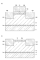
- 主面を有する基板と、
前記主面上に設けられ、メサ構造を有する電子走行層と、
前記メサ構造上に設けられ、前記電子走行層よりも大きいバンドギャップを有する障壁層と、
前記電子走行層上に設けられ、前記メサ構造及び前記障壁層の側面にそれぞれ接する二つの高濃度n型半導体領域と、
一方の前記高濃度n型半導体領域上に設けられたソース電極と、
他方の前記高濃度n型半導体領域上に設けられたドレイン電極と、
前記障壁層上に設けられたゲート電極と、
を備え、
前記障壁層の表面の水平位置は、前記高濃度n型半導体領域の各表面の水平位置よりも低く、
各高濃度n型半導体領域の前記表面のうち前記障壁層に隣接する一部と、前記障壁層の前記表面との成す角が135°以上160°以下の範囲内にある、高電子移動度トランジスタ。 - 各高濃度n型半導体領域がn型のZnO系化合物半導体領域である、請求項1に記載の高電子移動度トランジスタ。
- 前記基板がGaN基板、SiC基板、Si基板、及びサファイア基板のうち何れかであり、前記電子走行層がi型GaN層であり、前記障壁層がi型InAlN層である、請求項1または2に記載の高電子移動度トランジスタ。
- 電子走行層、及び前記電子走行層よりも大きいバンドギャップを有する障壁層を基板の主面上に順に成長させる工程と、
前記障壁層及び前記電子走行層をエッチングすることによりメサ構造を形成する工程と、
前記主面上に高濃度n型半導体層を形成する工程と、
前記メサ構造上に開口を有するマスクを前記高濃度n型半導体層上に形成する工程と、
前記マスクの前記開口を通じて前記メサ構造上の前記高濃度n型半導体層にウェットエッチングを施すことにより、高濃度n型半導体領域を形成する工程と、
前記メサ構造上にゲート電極を形成する工程と、
を含む、高電子移動度トランジスタの製造方法。 - 前記ゲート電極を形成する工程において、前記マスクを利用して前記ゲート電極を形成する、請求項4に記載の高電子移動度トランジスタの製造方法。
- 前記高濃度n型半導体層がn型のZnO系化合物半導体層であり、
前記高濃度n型半導体領域を形成する工程において、エッチャントとして希釈クエン酸、希釈アコニット酸、及び酢酸のうち少なくとも一つを用いる、請求項4または5に記載の高電子移動度トランジスタの製造方法。 - 前記電子走行層がi型GaN層であり、前記障壁層がi型InAlN層であり、
Cl2及びBCl3のうち少なくとも一方を用いたドライエッチングにより前記メサ構造を形成する、請求項4〜6のいずれか一項に記載の高電子移動度トランジスタの製造方法。
Priority Applications (2)
| Application Number | Priority Date | Filing Date | Title |
|---|---|---|---|
| JP2016048292A JP6690320B2 (ja) | 2016-03-11 | 2016-03-11 | 高電子移動度トランジスタ、及び高電子移動度トランジスタの製造方法 |
| US15/456,226 US10147811B2 (en) | 2016-03-11 | 2017-03-10 | Process of forming a high electron mobility transistor (HEMT) |
Applications Claiming Priority (1)
| Application Number | Priority Date | Filing Date | Title |
|---|---|---|---|
| JP2016048292A JP6690320B2 (ja) | 2016-03-11 | 2016-03-11 | 高電子移動度トランジスタ、及び高電子移動度トランジスタの製造方法 |
Publications (2)
| Publication Number | Publication Date |
|---|---|
| JP2017163082A true JP2017163082A (ja) | 2017-09-14 |
| JP6690320B2 JP6690320B2 (ja) | 2020-04-28 |
Family
ID=59787133
Family Applications (1)
| Application Number | Title | Priority Date | Filing Date |
|---|---|---|---|
| JP2016048292A Active JP6690320B2 (ja) | 2016-03-11 | 2016-03-11 | 高電子移動度トランジスタ、及び高電子移動度トランジスタの製造方法 |
Country Status (2)
| Country | Link |
|---|---|
| US (1) | US10147811B2 (ja) |
| JP (1) | JP6690320B2 (ja) |
Cited By (4)
| Publication number | Priority date | Publication date | Assignee | Title |
|---|---|---|---|---|
| JPWO2021029183A1 (ja) * | 2019-08-09 | 2021-02-18 | ||
| JP2021027165A (ja) * | 2019-08-05 | 2021-02-22 | 富士通株式会社 | 半導体装置、半導体装置の製造方法及び電子装置 |
| JP2022048690A (ja) * | 2020-09-15 | 2022-03-28 | 住友電気工業株式会社 | 半導体装置 |
| JP2024502520A (ja) * | 2021-12-13 | 2024-01-22 | 中国科学院蘇州納米技術与納米▲ファン▼生研究所 | 高電子移動度トランジスタ構造およびその製造方法並びに用途 |
Families Citing this family (7)
| Publication number | Priority date | Publication date | Assignee | Title |
|---|---|---|---|---|
| US10388753B1 (en) * | 2017-03-31 | 2019-08-20 | National Technology & Engineering Solutions Of Sandia, Llc | Regrowth method for fabricating wide-bandgap transistors, and devices made thereby |
| JP6828595B2 (ja) * | 2017-05-29 | 2021-02-10 | 三菱電機株式会社 | 半導体装置の製造方法 |
| JP7013710B2 (ja) * | 2017-08-07 | 2022-02-01 | 住友電気工業株式会社 | 窒化物半導体トランジスタの製造方法 |
| JP6977449B2 (ja) | 2017-09-27 | 2021-12-08 | 住友電気工業株式会社 | 電界効果トランジスタの製造方法及び電界効果トランジスタ |
| JP6879177B2 (ja) * | 2017-11-24 | 2021-06-02 | 住友電気工業株式会社 | 窒化物半導体素子の製造方法 |
| CN110112207B (zh) * | 2019-05-20 | 2020-05-05 | 中山大学 | 一种氧化镓基混合PiN肖特基二极管及其制备方法 |
| CN117751434A (zh) * | 2021-08-06 | 2024-03-22 | 华为技术有限公司 | 集成电路、功率放大电路及电子设备 |
Citations (11)
| Publication number | Priority date | Publication date | Assignee | Title |
|---|---|---|---|---|
| JPH03211839A (ja) * | 1989-12-31 | 1991-09-17 | Samsung Electron Co Ltd | 化合物半導体装置及びその製造方法 |
| JPH03250741A (ja) * | 1990-02-28 | 1991-11-08 | Fujitsu Ltd | 半導体装置の製造方法 |
| JPH05343435A (ja) * | 1992-06-08 | 1993-12-24 | Hitachi Ltd | 半導体装置 |
| JPH0661268A (ja) * | 1992-04-30 | 1994-03-04 | Mitsubishi Kasei Corp | 選択再成長領域を有する化合物半導体装置及びその製造方法 |
| JPH06267992A (ja) * | 1993-03-11 | 1994-09-22 | Hitachi Ltd | 半導体装置およびその製造方法 |
| JPH0888238A (ja) * | 1994-09-20 | 1996-04-02 | Hitachi Ltd | 化合物半導体電界効果トランジスタおよびそれを用いた化合物半導体集積回路 |
| JP2006313845A (ja) * | 2005-05-09 | 2006-11-16 | Rohm Co Ltd | 窒化物半導体素子およびその製法 |
| JP2007317856A (ja) * | 2006-05-25 | 2007-12-06 | Mitsubishi Gas Chem Co Inc | エッチング液組成物及びエッチング方法 |
| JP2007538402A (ja) * | 2004-05-20 | 2007-12-27 | クリー インコーポレイテッド | 再成長オーミックコンタクト領域を有する窒化物ベースのトランジスタの製作方法及び再成長オーミックコンタクト領域を有する窒化物ベースのトランジスタ |
| JP2008098455A (ja) * | 2006-10-13 | 2008-04-24 | Eudyna Devices Inc | 半導体装置 |
| JP2015523733A (ja) * | 2012-07-13 | 2015-08-13 | レイセオン カンパニー | 低オーム性コンタクト抵抗を有する窒化ガリウムデバイス |
Family Cites Families (6)
| Publication number | Priority date | Publication date | Assignee | Title |
|---|---|---|---|---|
| US7714359B2 (en) | 2005-02-17 | 2010-05-11 | Panasonic Corporation | Field effect transistor having nitride semiconductor layer |
| JP2006261642A (ja) | 2005-02-17 | 2006-09-28 | Matsushita Electric Ind Co Ltd | 電界効果トランジスタおよびその製造方法 |
| JP5076278B2 (ja) * | 2005-03-14 | 2012-11-21 | 日亜化学工業株式会社 | 電界効果トランジスタ |
| JP2012054471A (ja) * | 2010-09-02 | 2012-03-15 | Fujitsu Ltd | 半導体装置及びその製造方法、電源装置 |
| JP2012084739A (ja) * | 2010-10-13 | 2012-04-26 | Sumitomo Electric Ind Ltd | 半導体装置およびその製造方法 |
| US8324037B1 (en) * | 2011-09-28 | 2012-12-04 | Ishiang Shih | Fabrication methods for HEMT devices and circuits on compound semiconductor materials |
-
2016
- 2016-03-11 JP JP2016048292A patent/JP6690320B2/ja active Active
-
2017
- 2017-03-10 US US15/456,226 patent/US10147811B2/en active Active
Patent Citations (11)
| Publication number | Priority date | Publication date | Assignee | Title |
|---|---|---|---|---|
| JPH03211839A (ja) * | 1989-12-31 | 1991-09-17 | Samsung Electron Co Ltd | 化合物半導体装置及びその製造方法 |
| JPH03250741A (ja) * | 1990-02-28 | 1991-11-08 | Fujitsu Ltd | 半導体装置の製造方法 |
| JPH0661268A (ja) * | 1992-04-30 | 1994-03-04 | Mitsubishi Kasei Corp | 選択再成長領域を有する化合物半導体装置及びその製造方法 |
| JPH05343435A (ja) * | 1992-06-08 | 1993-12-24 | Hitachi Ltd | 半導体装置 |
| JPH06267992A (ja) * | 1993-03-11 | 1994-09-22 | Hitachi Ltd | 半導体装置およびその製造方法 |
| JPH0888238A (ja) * | 1994-09-20 | 1996-04-02 | Hitachi Ltd | 化合物半導体電界効果トランジスタおよびそれを用いた化合物半導体集積回路 |
| JP2007538402A (ja) * | 2004-05-20 | 2007-12-27 | クリー インコーポレイテッド | 再成長オーミックコンタクト領域を有する窒化物ベースのトランジスタの製作方法及び再成長オーミックコンタクト領域を有する窒化物ベースのトランジスタ |
| JP2006313845A (ja) * | 2005-05-09 | 2006-11-16 | Rohm Co Ltd | 窒化物半導体素子およびその製法 |
| JP2007317856A (ja) * | 2006-05-25 | 2007-12-06 | Mitsubishi Gas Chem Co Inc | エッチング液組成物及びエッチング方法 |
| JP2008098455A (ja) * | 2006-10-13 | 2008-04-24 | Eudyna Devices Inc | 半導体装置 |
| JP2015523733A (ja) * | 2012-07-13 | 2015-08-13 | レイセオン カンパニー | 低オーム性コンタクト抵抗を有する窒化ガリウムデバイス |
Cited By (6)
| Publication number | Priority date | Publication date | Assignee | Title |
|---|---|---|---|---|
| JP2021027165A (ja) * | 2019-08-05 | 2021-02-22 | 富士通株式会社 | 半導体装置、半導体装置の製造方法及び電子装置 |
| JPWO2021029183A1 (ja) * | 2019-08-09 | 2021-02-18 | ||
| JP2022048690A (ja) * | 2020-09-15 | 2022-03-28 | 住友電気工業株式会社 | 半導体装置 |
| JP7528664B2 (ja) | 2020-09-15 | 2024-08-06 | 住友電気工業株式会社 | 半導体装置 |
| JP2024502520A (ja) * | 2021-12-13 | 2024-01-22 | 中国科学院蘇州納米技術与納米▲ファン▼生研究所 | 高電子移動度トランジスタ構造およびその製造方法並びに用途 |
| JP7638024B2 (ja) | 2021-12-13 | 2025-03-03 | 中国科学院蘇州納米技術与納米▲ファン▼生研究所 | 高電子移動度トランジスタ構造およびその製造方法並びに用途 |
Also Published As
| Publication number | Publication date |
|---|---|
| JP6690320B2 (ja) | 2020-04-28 |
| US10147811B2 (en) | 2018-12-04 |
| US20170263743A1 (en) | 2017-09-14 |
Similar Documents
| Publication | Publication Date | Title |
|---|---|---|
| JP6690320B2 (ja) | 高電子移動度トランジスタ、及び高電子移動度トランジスタの製造方法 | |
| US9379191B2 (en) | High electron mobility transistor including an isolation region | |
| JP6018360B2 (ja) | 化合物半導体装置及びその製造方法 | |
| CN104009074B (zh) | 高电子迁移率晶体管及其制造方法 | |
| CN102651385B (zh) | 化合物半导体器件及其制造方法 | |
| JP6977449B2 (ja) | 電界効果トランジスタの製造方法及び電界効果トランジスタ | |
| JP6772729B2 (ja) | 高電子移動度トランジスタ、及び高電子移動度トランジスタの製造方法 | |
| US10784361B2 (en) | Semiconductor device and method for manufacturing the same | |
| JP6597046B2 (ja) | 高電子移動度トランジスタ | |
| US11908927B2 (en) | Nitride semiconductor device | |
| KR20070032701A (ko) | 재성장된 오믹 콘택 영역을 갖는 질화물계 트랜지스터의제조방법 및 재성장된 오믹 콘택 영역을 갖는 질화물계트랜지스터 | |
| US20130168686A1 (en) | High electron mobility transistor and method of forming the same | |
| JP2010192633A (ja) | GaN系電界効果トランジスタの製造方法 | |
| JP2011044647A (ja) | Iii族窒化物系電界効果トランジスタおよびその製造方法 | |
| JP2017059671A (ja) | 高電子移動度トランジスタ、及び高電子移動度トランジスタの製造方法 | |
| US20200185514A1 (en) | Semiconductor devices and methods for forming the same | |
| CN105470294A (zh) | 一种垂直型氮化镓功率开关器件及其制备方法 | |
| US20250142863A1 (en) | Method for manufacturing nitride semiconductor device and nitride semiconductor device | |
| US10373833B2 (en) | Semiconductor device and method for manufacturing the same | |
| JP5379391B2 (ja) | 窒化ガリウム系化合物半導体からなる半導体素子及びその製造方法 | |
| EP3405979B1 (en) | Semiconductor device, electronic part, electronic apparatus, and method for fabricating semiconductor device | |
| CN106531789A (zh) | 通过极性控制实现增强型hemt的方法及增强型hemt | |
| EP2933827B1 (en) | Transistor having nitride semiconductor used therein and method for manufacturing transistor having nitride semiconductor used therein | |
| JP2014229767A (ja) | ヘテロ接合電界効果型トランジスタ及びその製造方法 | |
| KR101678874B1 (ko) | 반도체 소자 제조방법 |
Legal Events
| Date | Code | Title | Description |
|---|---|---|---|
| A621 | Written request for application examination |
Free format text: JAPANESE INTERMEDIATE CODE: A621 Effective date: 20181221 |
|
| A977 | Report on retrieval |
Free format text: JAPANESE INTERMEDIATE CODE: A971007 Effective date: 20190905 |
|
| A131 | Notification of reasons for refusal |
Free format text: JAPANESE INTERMEDIATE CODE: A131 Effective date: 20190910 |
|
| A601 | Written request for extension of time |
Free format text: JAPANESE INTERMEDIATE CODE: A601 Effective date: 20191111 |
|
| A521 | Request for written amendment filed |
Free format text: JAPANESE INTERMEDIATE CODE: A523 Effective date: 20191210 |
|
| TRDD | Decision of grant or rejection written | ||
| A01 | Written decision to grant a patent or to grant a registration (utility model) |
Free format text: JAPANESE INTERMEDIATE CODE: A01 Effective date: 20200310 |
|
| A61 | First payment of annual fees (during grant procedure) |
Free format text: JAPANESE INTERMEDIATE CODE: A61 Effective date: 20200323 |
|
| R150 | Certificate of patent or registration of utility model |
Ref document number: 6690320 Country of ref document: JP Free format text: JAPANESE INTERMEDIATE CODE: R150 |
|
| R250 | Receipt of annual fees |
Free format text: JAPANESE INTERMEDIATE CODE: R250 |
|
| R250 | Receipt of annual fees |
Free format text: JAPANESE INTERMEDIATE CODE: R250 |
|
| R250 | Receipt of annual fees |
Free format text: JAPANESE INTERMEDIATE CODE: R250 |
|
| R250 | Receipt of annual fees |
Free format text: JAPANESE INTERMEDIATE CODE: R250 |