JP2017501431A - 基板上にパターン化された構造を形成するための方法およびシステム - Google Patents
基板上にパターン化された構造を形成するための方法およびシステム Download PDFInfo
- Publication number
- JP2017501431A JP2017501431A JP2016527224A JP2016527224A JP2017501431A JP 2017501431 A JP2017501431 A JP 2017501431A JP 2016527224 A JP2016527224 A JP 2016527224A JP 2016527224 A JP2016527224 A JP 2016527224A JP 2017501431 A JP2017501431 A JP 2017501431A
- Authority
- JP
- Japan
- Prior art keywords
- substrate
- donor
- light
- patterned
- donor substrate
- Prior art date
- Legal status (The legal status is an assumption and is not a legal conclusion. Google has not performed a legal analysis and makes no representation as to the accuracy of the status listed.)
- Granted
Links
Images


Classifications
-
- G—PHYSICS
- G03—PHOTOGRAPHY; CINEMATOGRAPHY; ANALOGOUS TECHNIQUES USING WAVES OTHER THAN OPTICAL WAVES; ELECTROGRAPHY; HOLOGRAPHY
- G03F—PHOTOMECHANICAL PRODUCTION OF TEXTURED OR PATTERNED SURFACES, e.g. FOR PRINTING, FOR PROCESSING OF SEMICONDUCTOR DEVICES; MATERIALS THEREFOR; ORIGINALS THEREFOR; APPARATUS SPECIALLY ADAPTED THEREFOR
- G03F7/00—Photomechanical, e.g. photolithographic, production of textured or patterned surfaces, e.g. printing surfaces; Materials therefor, e.g. comprising photoresists; Apparatus specially adapted therefor
- G03F7/20—Exposure; Apparatus therefor
- G03F7/2002—Exposure; Apparatus therefor with visible light or UV light, through an original having an opaque pattern on a transparent support, e.g. film printing, projection printing; by reflection of visible or UV light from an original such as a printed image
- G03F7/2008—Exposure; Apparatus therefor with visible light or UV light, through an original having an opaque pattern on a transparent support, e.g. film printing, projection printing; by reflection of visible or UV light from an original such as a printed image characterised by the reflectors, diffusers, light or heat filtering means or anti-reflective means used
-
- B—PERFORMING OPERATIONS; TRANSPORTING
- B41—PRINTING; LINING MACHINES; TYPEWRITERS; STAMPS
- B41M—PRINTING, DUPLICATING, MARKING, OR COPYING PROCESSES; COLOUR PRINTING
- B41M3/00—Printing processes to produce particular kinds of printed work, e.g. patterns
- B41M3/006—Patterns of chemical products used for a specific purpose, e.g. pesticides, perfumes, adhesive patterns; use of microencapsulated material; Printing on smoking articles
-
- B—PERFORMING OPERATIONS; TRANSPORTING
- B41—PRINTING; LINING MACHINES; TYPEWRITERS; STAMPS
- B41M—PRINTING, DUPLICATING, MARKING, OR COPYING PROCESSES; COLOUR PRINTING
- B41M5/00—Duplicating or marking methods; Sheet materials for use therein
- B41M5/26—Thermography ; Marking by high energetic means, e.g. laser otherwise than by burning, and characterised by the material used
- B41M5/40—Thermography ; Marking by high energetic means, e.g. laser otherwise than by burning, and characterised by the material used characterised by the base backcoat, intermediate, or covering layers, e.g. for thermal transfer dye-donor or dye-receiver sheets; Heat, radiation filtering or absorbing means or layers; combined with other image registration layers or compositions; Special originals for reproduction by thermography
- B41M5/46—Thermography ; Marking by high energetic means, e.g. laser otherwise than by burning, and characterised by the material used characterised by the base backcoat, intermediate, or covering layers, e.g. for thermal transfer dye-donor or dye-receiver sheets; Heat, radiation filtering or absorbing means or layers; combined with other image registration layers or compositions; Special originals for reproduction by thermography characterised by the light-to-heat converting means; characterised by the heat or radiation filtering or absorbing means or layers
-
- G—PHYSICS
- G03—PHOTOGRAPHY; CINEMATOGRAPHY; ANALOGOUS TECHNIQUES USING WAVES OTHER THAN OPTICAL WAVES; ELECTROGRAPHY; HOLOGRAPHY
- G03F—PHOTOMECHANICAL PRODUCTION OF TEXTURED OR PATTERNED SURFACES, e.g. FOR PRINTING, FOR PROCESSING OF SEMICONDUCTOR DEVICES; MATERIALS THEREFOR; ORIGINALS THEREFOR; APPARATUS SPECIALLY ADAPTED THEREFOR
- G03F7/00—Photomechanical, e.g. photolithographic, production of textured or patterned surfaces, e.g. printing surfaces; Materials therefor, e.g. comprising photoresists; Apparatus specially adapted therefor
- G03F7/70—Microphotolithographic exposure; Apparatus therefor
- G03F7/70058—Mask illumination systems
- G03F7/7015—Details of optical elements
-
- H—ELECTRICITY
- H10—SEMICONDUCTOR DEVICES; ELECTRIC SOLID-STATE DEVICES NOT OTHERWISE PROVIDED FOR
- H10K—ORGANIC ELECTRIC SOLID-STATE DEVICES
- H10K71/00—Manufacture or treatment specially adapted for the organic devices covered by this subclass
- H10K71/10—Deposition of organic active material
- H10K71/18—Deposition of organic active material using non-liquid printing techniques, e.g. thermal transfer printing from a donor sheet
-
- B—PERFORMING OPERATIONS; TRANSPORTING
- B41—PRINTING; LINING MACHINES; TYPEWRITERS; STAMPS
- B41M—PRINTING, DUPLICATING, MARKING, OR COPYING PROCESSES; COLOUR PRINTING
- B41M2205/00—Printing methods or features related to printing methods; Location or type of the layers
- B41M2205/14—Production or use of a mask
Landscapes
- Physics & Mathematics (AREA)
- General Chemical & Material Sciences (AREA)
- Optics & Photonics (AREA)
- Life Sciences & Earth Sciences (AREA)
- Chemical & Material Sciences (AREA)
- Chemical Kinetics & Catalysis (AREA)
- Pest Control & Pesticides (AREA)
- General Physics & Mathematics (AREA)
- Engineering & Computer Science (AREA)
- Manufacturing & Machinery (AREA)
- Manufacturing Of Printed Wiring (AREA)
- Electroluminescent Light Sources (AREA)
- Exposure And Positioning Against Photoresist Photosensitive Materials (AREA)
- Application Of Or Painting With Fluid Materials (AREA)
Abstract
Description
1.チップ接着パッドの高解像度および高アスペクト比のパターン化(<0.5ms)。
2.導電性インクのフォトニック焼結(約10ms)。
3.接着パッド上へのはんだバンプの設置(<0.5ms)。
4.チップ設置後のフォトニックはんだ付け(2ms)。
5.横漏れを避けるためのトレンチ充填(<0.5ms)。
− 光パルス:広帯域フラッシュランプ。転写された液滴の温度を制御するために変調される。
− 光学系:高エッジシャープネスおよび高解像度を得るために好ましいコリメートされた光ビーム。
− 画素化マスク:ガラス上のフォトリソグラフィ処理された(photolithographed)金属。光吸収およびアブレーションの機会を低減するためのアルミニウムまたはクロム。
− 位置合わせ(オプションの):はんだバンプの設置およびトレンチの充填のために、位置合わせシステムが、好ましい。
− 基板:ポリマーフィルム、ガラス。光について透明。
− インク:ランプ発光スペクトルに関して高吸光度を有する、溶剤に基づくインク。せん断薄化ペースト(shear thinning paste)は、低粘性インクと同様に機能するはずである。
− アクセプタ基板:任意の種類。アクセプタとドナーとの間のギャップは、転写された液滴の温度/時間プロファイルにとって重要である。
− ランプ装置:Xenon Sinteron(登録商標)2000。
− パルス:500μs、約5J/cm2、1パルス。
− マスク:イーグルガラス(eagle glass)(0.7mm)上のクロム(100nm)。
− ドナー:PEN、25μm厚さ。
− インク:DuPont X115、サブミクロンのスクリーン印刷ペースト。
− ギャップ:600μm。
− アクセプタ基板:ガラス、1.1mm。
− 光源:キセノンフラッシュランプ。最適結果のために好ましい高エネルギーの短パルス(<<500μs)。
− マスク:ガラス上のフォトリソグラフィ処理された金属。光吸収およびアブレーションの機会を低減するためのアルミニウムまたはクロム。
− ドナー基板:ポリマーフィルム、ガラス。光について透明。
− インク:キセノン発光スペクトルに関して高吸光度を有する、溶剤に基づくインク。粘度は、変化することもあるが、しかし例えば固体材料の転写は、より困難となり得る。
− 剥離層:この層の劣化は、アクセプタ基板に向かってインクを放出することもある。この層は、プロセスを改善することができ、それは、完全な(OLED/OPV)スタックを転写することさえできることもある。
− アクセプタ基板:任意の種類。ドナー基板とアクセプタ基板との間の距離は、例えば変調パルスを使用することを考慮して設定されてもよい。
− ランプ装置:Xenon Sinteron(登録商標)2000。
− パルス:500μs、約4J/cm2、1パルス。
− マスク:イーグルガラス(0.7mm)上のアルミニウム(100nm)。
− ドナー基板:イーグルガラスおよびPEN。
− インク:DuPont(登録商標) 5025およびSuntronic(登録商標) U5714。
− アクセプタ基板:PENフィルム(125μm)。
− ギャップ:1mm。
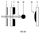
2 剥離層
3 ドナー材料
3d 液滴
3d’ 破片
3p パターン化された構造
3p’ 不規則なパターン化された構造
3t ドナー材料の層厚さ
4 アクセプタ基板
5 光源
6 光
6b ビーム
6c ビームのサイズ
6d ビーム間の分離距離
6p パターン化された光
6p’ パターン化された光
7 マスク
7’ 従来のマスク
7a パターンエリア
7a’ 大きい連続エリア、回路部分
7p マスクパターン
7p’ 従来のマスクパターン
10 ドナー基板
11 手段、運搬装置
14 手段、運搬装置
30 システム
C1 パターンエリアサイズ
C2 パターンエリアサイズ
C3 パターンエリアサイズ
I1 第1の光強度
I2 第2の光強度
I3 第3の光強度
P 変調パルス
R1 領域
R2 領域
R3 領域
R4 領域
T1 第1の時間間隔
T2 第2の時間間隔
T3 第3の時間間隔
X1 第1の寸法
X2 画素間の分離距離
Y1 第2の寸法
Y2 画素間の分離距離
Claims (15)
- 基板上にパターン化された構造(3p)を提供するための方法であって、
光源(5)とアクセプタ基板(4)との間に配置されるドナー基板(10)を準備するステップであって、前記ドナー基板(10)は、ドナー材料(3)を備える、ステップと、
前記光源(5)と前記ドナー基板(10)との間に配置されるマスク(7)を準備するステップであって、前記マスク(7)は、前記ドナー基板(10)に衝突する前記光源(5)からの光(6)をパターン化するためにマスクパターン(7p)を備え、前記パターン化された光(6p)は、作成すべき前記パターン化された構造(3p)に合致し、前記ドナー基板(10)に衝突する前記パターン化された光(6p)は、前記ドナー材料(3)を前記ドナー基板(10)から剥離させ、前記アクセプタ基板(4)に転写し、前記パターン化された構造(3p)をその上に形成させる、ステップとを含み、
前記パターン化された光(6p)は、前記ドナー基板(10)から別個の均一なサイズの液滴(3d)の形で前記ドナー材料(3)を剥離させるために、前記ドナー基板(10)に同時に衝突する複数の別個の均一なサイズのビーム(6b)に分割される、方法。 - 前記マスクパターン(7p)は、形成すべき前記パターン化された構造(3p)のエリアの異なるサイズに対応する異なるサイズ(C1、C2)を有する複数のパターンエリア(7a)を備え、パターンエリア(7a)によってパターン化される前記光は、複数の別個の均一なサイズの隣接するビーム(6b)に分割され、その隣接するビームは、前記アクセプタ基板(4)上に前記パターン化された構造(3p)の相互接続エリアを形成する、請求項1に記載の方法。
- 前記マスク(7)は、
形成すべき異なるサイズの回路要素に対応する異なるサイズ(C1、C2)を有する複数のパターンエリア(7a)を備えるマスクパターン(7p)を受け取り、かつ
前記パターンエリア(7a)を複数の別個の均一なサイズの画素に分割することによって作られる、請求項1または2に記載の方法。 - 前記ビーム(6b)は、前記アクセプタ基板(4)上で均一な距離に前記液滴(3d)を堆積するために均一に距離を置かれ(6d)、相互接続パターン化された構造(3p)は、前記アクセプタ基板(4)上に広がりかつ隣接する転写された液滴に接続する転写された液滴によって形成される、請求項1から3のいずれか一項に記載の方法。
- 前記ドナー基板(10)に衝突するビーム(6b)のサイズ(6c)は、前記ドナー基板(10)上の前記ドナー材料(3)の層厚さ(3t)の150〜250%である、請求項1から4のいずれか一項に記載の方法。
- 隣接するビーム間の分離距離(6d)は、前記ビームのサイズ(6c)の10から150%の間である、請求項1から5のいずれか一項に記載の方法。
- 前記ビームは、第1の寸法(X1)および前記第1の寸法(X1)に等しい横断方向の第2の寸法(Y1)を有する、請求項1から6のいずれか一項に記載の方法。
- 前記光源(5)は、フラッシュランプを備える、請求項1から7のいずれか一項に記載の方法。
- 前記光(6)は、変調パルス(P)を備え、前記変調は、第1の時間間隔(T1)および前記第1の時間間隔(T1)よりも長い第2の時間間隔(T2)を備え、前記第1の時間間隔(T1)において、前記変調パルスは、前記ドナー材料を剥離するために第1の光強度(I1)を有し、前記第2の時間間隔(T2)において、前記変調パルスは、前記ドナー材料が前記ドナー基板とアクセプタ基板との間を通過している間に前記ドナー材料を乾燥し、溶融し、かつ/または焼結するために前記第1の光強度(I1)よりも低い第2の光強度(I2)を有する、請求項1から8のいずれか一項に記載の方法。
- 前記ドナー基板(10)は、前記ドナー基板(10)とアクセプタ基板(4)との間でその面上に配置されるドナー材料(3)の層を有する透明基板(1)を備える、請求項1から9のいずれか一項に記載の方法。
- 前記ドナー基板(10)は、透明基板(1)とドナー材料(3)の前記層との間に剥離層(2)を備え、前記剥離層(2)は、前記ドナー基板(10)から前記ドナー材料(3)を剥離するために前記光(6)の影響下で反応する、請求項1から10のいずれか一項に記載の方法。
- 基板上にパターン化された構造(3p)を提供するためのシステム(30)であって、
光源(5)と、
前記パターン化された構造(3p)を受け取るためにアクセプタ基板(4)を提供するための手段(14)と、
ドナー材料(3)を備えるドナー基板(10)を提供するための手段(11)であって、前記ドナー基板(10)は、前記光源(5)と前記アクセプタ基板(4)との間に配置される、手段(11)と、
前記光源(5)と前記ドナー基板(10)との間に配置されるマスク(7)であって、前記ドナー基板(10)に衝突する前記光源(5)からの光(6)をパターン化するためにマスクパターン(7p)を備え、前記パターン化された光(6p)は、作成すべき前記パターン化された構造(3p)に合致し、前記ドナー基板(10)に衝突する前記パターン化された光(6p)は、前記ドナー材料(3)を前記ドナー基板(10)から剥離させ、前記アクセプタ基板(4)に転写し、前記パターン化された構造(3p)をその上に形成させるように適合される、マスク(7)とを備え、
前記パターン化された光(6p)は、前記ドナー基板(10)から別個の均一なサイズの液滴(3d)の形で前記ドナー材料(3)を剥離させるために、前記ドナー基板(10)に同時に衝突する複数の別個の均一なサイズのビーム(6b)に分割される、システム(30)。 - 前記ビーム(6b)は、前記アクセプタ基板(4)上で均一な距離に前記液滴(3d)を堆積するために均一に距離を置かれ(6d)、相互接続パターン化された構造(3p)は、前記アクセプタ基板(4)上に広がりかつ隣接する転写された液滴に接続する転写された液滴によって形成される、請求項12に記載のシステム(30)。
- 前記マスクパターン(7p)は、形成すべき前記パターン化された構造(3p)のエリアの異なるサイズに対応する異なるサイズ(C1、C2)を有する複数のパターンエリア(7a)を備え、前記マスクパターン(7p)は、別個の画素(P)に分割され、複数の隣接する画素(P)は、前記複数のパターンエリア(7a)の1つのパターンエリアを形成するように配置される、請求項12または13に記載のシステム(30)。
- 前記光源(5)は、フラッシュランプを備える、請求項12から14のいずれか一項に記載のシステム(30)。
Applications Claiming Priority (5)
| Application Number | Priority Date | Filing Date | Title |
|---|---|---|---|
| EP13190956.6 | 2013-10-30 | ||
| EP13190956 | 2013-10-30 | ||
| EP13197502.1 | 2013-12-16 | ||
| EP13197502.1A EP2883709A1 (en) | 2013-12-16 | 2013-12-16 | Method and system for forming a patterned structure on a substrate |
| PCT/NL2014/050748 WO2015065182A1 (en) | 2013-10-30 | 2014-10-29 | Method and system for forming a patterned structure on a substrate |
Publications (2)
| Publication Number | Publication Date |
|---|---|
| JP2017501431A true JP2017501431A (ja) | 2017-01-12 |
| JP6549571B2 JP6549571B2 (ja) | 2019-07-24 |
Family
ID=51871259
Family Applications (1)
| Application Number | Title | Priority Date | Filing Date |
|---|---|---|---|
| JP2016527224A Expired - Fee Related JP6549571B2 (ja) | 2013-10-30 | 2014-10-29 | 基板上にパターン化された構造を形成するための方法およびシステム |
Country Status (7)
| Country | Link |
|---|---|
| US (1) | US10338473B2 (ja) |
| EP (1) | EP3063014B1 (ja) |
| JP (1) | JP6549571B2 (ja) |
| KR (1) | KR102292841B1 (ja) |
| CN (1) | CN105916696B (ja) |
| TW (1) | TWI636896B (ja) |
| WO (1) | WO2015065182A1 (ja) |
Cited By (2)
| Publication number | Priority date | Publication date | Assignee | Title |
|---|---|---|---|---|
| JP2019530017A (ja) * | 2016-08-26 | 2019-10-17 | ネーデルラントセ オルハニサティエ フォール トゥーヘパスト−ナトゥールヴェッテンシャッペリーク オンデルズック テーエヌオー | 表面にパターン構造をアプライするための方法およびシステム |
| WO2025216114A1 (ja) * | 2024-04-09 | 2025-10-16 | 株式会社村田製作所 | セラミック基板およびその製造方法ならびにモジュール |
Families Citing this family (5)
| Publication number | Priority date | Publication date | Assignee | Title |
|---|---|---|---|---|
| EP3058113B1 (en) * | 2013-10-14 | 2020-12-02 | Orbotech Ltd. | Lift printing of multi-composition material structures |
| CN109690757B (zh) | 2016-10-04 | 2023-02-28 | 维耶尔公司 | 施体衬底中的微装置布置 |
| EP3663090A1 (en) * | 2018-12-04 | 2020-06-10 | Nederlandse Organisatie voor toegepast- natuurwetenschappelijk onderzoek TNO | High resolution laser induced forward transfer |
| CN115702488A (zh) * | 2020-06-04 | 2023-02-14 | 奥宝科技有限公司 | 高分辨率焊接 |
| FR3141091A1 (fr) | 2022-10-20 | 2024-04-26 | Poietis | Impression d’objets a partir d’un puits |
Citations (5)
| Publication number | Priority date | Publication date | Assignee | Title |
|---|---|---|---|---|
| JPH07273003A (ja) * | 1994-03-29 | 1995-10-20 | Hitachi Ltd | パターン転写装置 |
| JP2007206675A (ja) * | 2006-01-16 | 2007-08-16 | Samsung Sdi Co Ltd | レーザー照射装置及びこれを利用した有機電界発光素子の製造方法 |
| JP2007534012A (ja) * | 2004-04-10 | 2007-11-22 | イーストマン コダック カンパニー | レリーフ画像の製造方法 |
| JP2008053698A (ja) * | 2006-07-28 | 2008-03-06 | Semiconductor Energy Lab Co Ltd | 半導体装置の作製方法 |
| JP2010533977A (ja) * | 2007-07-17 | 2010-10-28 | スリーエム イノベイティブ プロパティズ カンパニー | 基材のパターニング方法 |
Family Cites Families (13)
| Publication number | Priority date | Publication date | Assignee | Title |
|---|---|---|---|---|
| US4458003A (en) * | 1982-06-07 | 1984-07-03 | Esselte Pendaflex Corp. | Photosensitive materials for use in making dry transfers |
| US5229232A (en) * | 1991-08-05 | 1993-07-20 | Eastman Kodak Company | Method of making thermally-transferred color filter arrays with incorporated black matrix using electronic light flash |
| US5693447A (en) * | 1995-02-17 | 1997-12-02 | Konica Corporation | Image forming material, method of preparing the same and image forming method employing the same |
| US6529284B1 (en) * | 1998-08-07 | 2003-03-04 | Texas Instruments Incorporated | Efficient rendering of masks to a screened buffer using a lookup table |
| US6358664B1 (en) * | 2000-09-15 | 2002-03-19 | 3M Innovative Properties Company | Electronically active primer layers for thermal patterning of materials for electronic devices |
| US6918982B2 (en) * | 2002-12-09 | 2005-07-19 | International Business Machines Corporation | System and method of transfer printing an organic semiconductor |
| US7381579B2 (en) * | 2004-02-26 | 2008-06-03 | Samsung Sdi Co., Ltd. | Donor sheet, method of manufacturing the same, method of manufacturing TFT using the donor sheet, and method of manufacturing flat panel display device using the donor sheet |
| KR100667069B1 (ko) * | 2004-10-19 | 2007-01-10 | 삼성에스디아이 주식회사 | 도너 기판 및 그를 사용한 유기전계발광표시장치의 제조방법 |
| GB2438601B (en) * | 2006-05-24 | 2008-04-09 | Exitech Ltd | Method and unit for micro-structuring a moving substrate |
| US7994021B2 (en) | 2006-07-28 | 2011-08-09 | Semiconductor Energy Laboratory Co., Ltd. | Method of manufacturing semiconductor device |
| US8435723B2 (en) * | 2008-09-11 | 2013-05-07 | Nikon Corporation | Pattern forming method and device production method |
| KR20140118004A (ko) * | 2013-03-27 | 2014-10-08 | 삼성디스플레이 주식회사 | 도너 기판 제조방법 |
| KR20140133741A (ko) * | 2013-05-10 | 2014-11-20 | 삼성디스플레이 주식회사 | 레이저 열전사용 마스크 및 이를 포함하는 레이저 조사 장치 |
-
2014
- 2014-10-22 TW TW103136473A patent/TWI636896B/zh not_active IP Right Cessation
- 2014-10-29 JP JP2016527224A patent/JP6549571B2/ja not_active Expired - Fee Related
- 2014-10-29 KR KR1020167013213A patent/KR102292841B1/ko not_active Expired - Fee Related
- 2014-10-29 US US15/032,950 patent/US10338473B2/en not_active Expired - Fee Related
- 2014-10-29 CN CN201480070602.2A patent/CN105916696B/zh not_active Expired - Fee Related
- 2014-10-29 EP EP14796304.5A patent/EP3063014B1/en not_active Not-in-force
- 2014-10-29 WO PCT/NL2014/050748 patent/WO2015065182A1/en not_active Ceased
Patent Citations (5)
| Publication number | Priority date | Publication date | Assignee | Title |
|---|---|---|---|---|
| JPH07273003A (ja) * | 1994-03-29 | 1995-10-20 | Hitachi Ltd | パターン転写装置 |
| JP2007534012A (ja) * | 2004-04-10 | 2007-11-22 | イーストマン コダック カンパニー | レリーフ画像の製造方法 |
| JP2007206675A (ja) * | 2006-01-16 | 2007-08-16 | Samsung Sdi Co Ltd | レーザー照射装置及びこれを利用した有機電界発光素子の製造方法 |
| JP2008053698A (ja) * | 2006-07-28 | 2008-03-06 | Semiconductor Energy Lab Co Ltd | 半導体装置の作製方法 |
| JP2010533977A (ja) * | 2007-07-17 | 2010-10-28 | スリーエム イノベイティブ プロパティズ カンパニー | 基材のパターニング方法 |
Cited By (4)
| Publication number | Priority date | Publication date | Assignee | Title |
|---|---|---|---|---|
| JP2019530017A (ja) * | 2016-08-26 | 2019-10-17 | ネーデルラントセ オルハニサティエ フォール トゥーヘパスト−ナトゥールヴェッテンシャッペリーク オンデルズック テーエヌオー | 表面にパターン構造をアプライするための方法およびシステム |
| US11173737B2 (en) | 2016-08-26 | 2021-11-16 | Nederlandse Organisatie Voor Toegepast-Natuurwetenschappelijk Onderzoek Tno | Method and system for applying a patterned structure on a surface |
| JP7029455B2 (ja) | 2016-08-26 | 2022-03-03 | ネーデルラントセ オルハニサティエ フォール トゥーヘパスト-ナトゥールヴェッテンシャッペリーク オンデルズック テーエヌオー | 表面にパターン構造をアプライするための方法およびシステム |
| WO2025216114A1 (ja) * | 2024-04-09 | 2025-10-16 | 株式会社村田製作所 | セラミック基板およびその製造方法ならびにモジュール |
Also Published As
| Publication number | Publication date |
|---|---|
| WO2015065182A1 (en) | 2015-05-07 |
| US10338473B2 (en) | 2019-07-02 |
| KR102292841B1 (ko) | 2021-08-25 |
| KR20160078383A (ko) | 2016-07-04 |
| EP3063014A1 (en) | 2016-09-07 |
| EP3063014B1 (en) | 2019-09-11 |
| US20160259250A1 (en) | 2016-09-08 |
| CN105916696A (zh) | 2016-08-31 |
| JP6549571B2 (ja) | 2019-07-24 |
| CN105916696B (zh) | 2018-08-17 |
| TWI636896B (zh) | 2018-10-01 |
| TW201534488A (zh) | 2015-09-16 |
Similar Documents
| Publication | Publication Date | Title |
|---|---|---|
| JP6549571B2 (ja) | 基板上にパターン化された構造を形成するための方法およびシステム | |
| JP7561771B2 (ja) | 部品の光誘起型の選択的転写 | |
| KR102830402B1 (ko) | 디스플레이 장치의 제조 방법, 및 소스 기판 구조체 | |
| US11374149B2 (en) | Method of manufacturing display device and source substrate structure | |
| EP2917931B1 (en) | Method for bonding bare chip dies | |
| JP7443236B2 (ja) | Lift堆積装置及び方法 | |
| TW202008558A (zh) | 晶片轉移之方法及其晶片轉移系統 | |
| CN109922968B (zh) | 用于在表面上施加图案化结构的方法和系统 | |
| KR20100110447A (ko) | 레이저 직접 박막 패터닝 방법 | |
| JP2011233711A (ja) | 半導体装置の製造方法 | |
| CN102983289A (zh) | 用于无掩模封装的方法 | |
| JP2015026655A (ja) | 薄膜形成方法及び薄膜形成装置 | |
| JP6222113B2 (ja) | 薄膜形成方法及び薄膜形成装置 | |
| JPWO2020222090A5 (ja) | ||
| EP2883709A1 (en) | Method and system for forming a patterned structure on a substrate | |
| KR102212422B1 (ko) | 희생층을 이용한 광 유도 전사 방법 | |
| JP2012151394A (ja) | 射出装置およびパターン形成装置、並びに、射出方法およびパターン形成方法 |
Legal Events
| Date | Code | Title | Description |
|---|---|---|---|
| A621 | Written request for application examination |
Free format text: JAPANESE INTERMEDIATE CODE: A621 Effective date: 20171017 |
|
| A977 | Report on retrieval |
Free format text: JAPANESE INTERMEDIATE CODE: A971007 Effective date: 20180928 |
|
| A131 | Notification of reasons for refusal |
Free format text: JAPANESE INTERMEDIATE CODE: A131 Effective date: 20181005 |
|
| A601 | Written request for extension of time |
Free format text: JAPANESE INTERMEDIATE CODE: A601 Effective date: 20181226 |
|
| A521 | Request for written amendment filed |
Free format text: JAPANESE INTERMEDIATE CODE: A523 Effective date: 20190402 |
|
| TRDD | Decision of grant or rejection written | ||
| A01 | Written decision to grant a patent or to grant a registration (utility model) |
Free format text: JAPANESE INTERMEDIATE CODE: A01 Effective date: 20190603 |
|
| A61 | First payment of annual fees (during grant procedure) |
Free format text: JAPANESE INTERMEDIATE CODE: A61 Effective date: 20190627 |
|
| R150 | Certificate of patent or registration of utility model |
Ref document number: 6549571 Country of ref document: JP Free format text: JAPANESE INTERMEDIATE CODE: R150 |
|
| LAPS | Cancellation because of no payment of annual fees |