JP2019013960A - 導電性ボール及び電子装置とそれらの製造方法 - Google Patents
導電性ボール及び電子装置とそれらの製造方法 Download PDFInfo
- Publication number
- JP2019013960A JP2019013960A JP2017133267A JP2017133267A JP2019013960A JP 2019013960 A JP2019013960 A JP 2019013960A JP 2017133267 A JP2017133267 A JP 2017133267A JP 2017133267 A JP2017133267 A JP 2017133267A JP 2019013960 A JP2019013960 A JP 2019013960A
- Authority
- JP
- Japan
- Prior art keywords
- layer
- solder
- connection pad
- tin
- conductive ball
- Prior art date
- Legal status (The legal status is an assumption and is not a legal conclusion. Google has not performed a legal analysis and makes no representation as to the accuracy of the status listed.)
- Granted
Links
Images


Classifications
-
- B—PERFORMING OPERATIONS; TRANSPORTING
- B23—MACHINE TOOLS; METAL-WORKING NOT OTHERWISE PROVIDED FOR
- B23K—SOLDERING OR UNSOLDERING; WELDING; CLADDING OR PLATING BY SOLDERING OR WELDING; CUTTING BY APPLYING HEAT LOCALLY, e.g. FLAME CUTTING; WORKING BY LASER BEAM
- B23K35/00—Rods, electrodes, materials, or media, for use in soldering, welding, or cutting
- B23K35/02—Rods, electrodes, materials, or media, for use in soldering, welding, or cutting characterised by mechanical features, e.g. shape
- B23K35/0222—Rods, electrodes, materials, or media, for use in soldering, welding, or cutting characterised by mechanical features, e.g. shape for use in soldering or brazing
- B23K35/0244—Powders, particles or spheres; Preforms made therefrom
-
- B—PERFORMING OPERATIONS; TRANSPORTING
- B23—MACHINE TOOLS; METAL-WORKING NOT OTHERWISE PROVIDED FOR
- B23K—SOLDERING OR UNSOLDERING; WELDING; CLADDING OR PLATING BY SOLDERING OR WELDING; CUTTING BY APPLYING HEAT LOCALLY, e.g. FLAME CUTTING; WORKING BY LASER BEAM
- B23K35/00—Rods, electrodes, materials, or media, for use in soldering, welding, or cutting
- B23K35/22—Rods, electrodes, materials, or media, for use in soldering, welding, or cutting characterised by the composition or nature of the material
- B23K35/24—Selection of soldering or welding materials proper
- B23K35/26—Selection of soldering or welding materials proper with the principal constituent melting at less than 400°C
- B23K35/262—Sn as the principal constituent
-
- C—CHEMISTRY; METALLURGY
- C22—METALLURGY; FERROUS OR NON-FERROUS ALLOYS; TREATMENT OF ALLOYS OR NON-FERROUS METALS
- C22C—ALLOYS
- C22C30/00—Alloys containing less than 50% by weight of each constituent
- C22C30/02—Alloys containing less than 50% by weight of each constituent containing copper
-
- C—CHEMISTRY; METALLURGY
- C22—METALLURGY; FERROUS OR NON-FERROUS ALLOYS; TREATMENT OF ALLOYS OR NON-FERROUS METALS
- C22C—ALLOYS
- C22C30/00—Alloys containing less than 50% by weight of each constituent
- C22C30/04—Alloys containing less than 50% by weight of each constituent containing tin or lead
-
- B—PERFORMING OPERATIONS; TRANSPORTING
- B23—MACHINE TOOLS; METAL-WORKING NOT OTHERWISE PROVIDED FOR
- B23K—SOLDERING OR UNSOLDERING; WELDING; CLADDING OR PLATING BY SOLDERING OR WELDING; CUTTING BY APPLYING HEAT LOCALLY, e.g. FLAME CUTTING; WORKING BY LASER BEAM
- B23K2101/00—Articles made by soldering, welding or cutting
- B23K2101/36—Electric or electronic devices
-
- H—ELECTRICITY
- H10—SEMICONDUCTOR DEVICES; ELECTRIC SOLID-STATE DEVICES NOT OTHERWISE PROVIDED FOR
- H10W—GENERIC PACKAGES, INTERCONNECTIONS, CONNECTORS OR OTHER CONSTRUCTIONAL DETAILS OF DEVICES COVERED BY CLASS H10
- H10W72/00—Interconnections or connectors in packages
- H10W72/01—Manufacture or treatment
- H10W72/012—Manufacture or treatment of bump connectors, dummy bumps or thermal bumps
- H10W72/01221—Manufacture or treatment of bump connectors, dummy bumps or thermal bumps using local deposition
- H10W72/01225—Manufacture or treatment of bump connectors, dummy bumps or thermal bumps using local deposition in solid form, e.g. by using a powder or by stud bumping
-
- H—ELECTRICITY
- H10—SEMICONDUCTOR DEVICES; ELECTRIC SOLID-STATE DEVICES NOT OTHERWISE PROVIDED FOR
- H10W—GENERIC PACKAGES, INTERCONNECTIONS, CONNECTORS OR OTHER CONSTRUCTIONAL DETAILS OF DEVICES COVERED BY CLASS H10
- H10W72/00—Interconnections or connectors in packages
- H10W72/01—Manufacture or treatment
- H10W72/012—Manufacture or treatment of bump connectors, dummy bumps or thermal bumps
- H10W72/01231—Manufacture or treatment of bump connectors, dummy bumps or thermal bumps using blanket deposition
- H10W72/01233—Manufacture or treatment of bump connectors, dummy bumps or thermal bumps using blanket deposition in liquid form, e.g. spin coating, spray coating or immersion coating
- H10W72/01235—Manufacture or treatment of bump connectors, dummy bumps or thermal bumps using blanket deposition in liquid form, e.g. spin coating, spray coating or immersion coating by plating, e.g. electroless plating or electroplating
-
- H—ELECTRICITY
- H10—SEMICONDUCTOR DEVICES; ELECTRIC SOLID-STATE DEVICES NOT OTHERWISE PROVIDED FOR
- H10W—GENERIC PACKAGES, INTERCONNECTIONS, CONNECTORS OR OTHER CONSTRUCTIONAL DETAILS OF DEVICES COVERED BY CLASS H10
- H10W72/00—Interconnections or connectors in packages
- H10W72/071—Connecting or disconnecting
- H10W72/072—Connecting or disconnecting of bump connectors
- H10W72/07231—Techniques
- H10W72/07236—Soldering or alloying
-
- H—ELECTRICITY
- H10—SEMICONDUCTOR DEVICES; ELECTRIC SOLID-STATE DEVICES NOT OTHERWISE PROVIDED FOR
- H10W—GENERIC PACKAGES, INTERCONNECTIONS, CONNECTORS OR OTHER CONSTRUCTIONAL DETAILS OF DEVICES COVERED BY CLASS H10
- H10W72/00—Interconnections or connectors in packages
- H10W72/20—Bump connectors, e.g. solder bumps or copper pillars; Dummy bumps; Thermal bumps
- H10W72/221—Structures or relative sizes
- H10W72/222—Multilayered bumps, e.g. a coating on top and side surfaces of a bump core
-
- H—ELECTRICITY
- H10—SEMICONDUCTOR DEVICES; ELECTRIC SOLID-STATE DEVICES NOT OTHERWISE PROVIDED FOR
- H10W—GENERIC PACKAGES, INTERCONNECTIONS, CONNECTORS OR OTHER CONSTRUCTIONAL DETAILS OF DEVICES COVERED BY CLASS H10
- H10W72/00—Interconnections or connectors in packages
- H10W72/20—Bump connectors, e.g. solder bumps or copper pillars; Dummy bumps; Thermal bumps
- H10W72/231—Shapes
- H10W72/232—Plan-view shape, i.e. in top view
-
- H—ELECTRICITY
- H10—SEMICONDUCTOR DEVICES; ELECTRIC SOLID-STATE DEVICES NOT OTHERWISE PROVIDED FOR
- H10W—GENERIC PACKAGES, INTERCONNECTIONS, CONNECTORS OR OTHER CONSTRUCTIONAL DETAILS OF DEVICES COVERED BY CLASS H10
- H10W72/00—Interconnections or connectors in packages
- H10W72/20—Bump connectors, e.g. solder bumps or copper pillars; Dummy bumps; Thermal bumps
- H10W72/241—Dispositions, e.g. layouts
-
- H—ELECTRICITY
- H10—SEMICONDUCTOR DEVICES; ELECTRIC SOLID-STATE DEVICES NOT OTHERWISE PROVIDED FOR
- H10W—GENERIC PACKAGES, INTERCONNECTIONS, CONNECTORS OR OTHER CONSTRUCTIONAL DETAILS OF DEVICES COVERED BY CLASS H10
- H10W72/00—Interconnections or connectors in packages
- H10W72/20—Bump connectors, e.g. solder bumps or copper pillars; Dummy bumps; Thermal bumps
- H10W72/251—Materials
- H10W72/252—Materials comprising solid metals or solid metalloids, e.g. PbSn, Ag or Cu
-
- H—ELECTRICITY
- H10—SEMICONDUCTOR DEVICES; ELECTRIC SOLID-STATE DEVICES NOT OTHERWISE PROVIDED FOR
- H10W—GENERIC PACKAGES, INTERCONNECTIONS, CONNECTORS OR OTHER CONSTRUCTIONAL DETAILS OF DEVICES COVERED BY CLASS H10
- H10W72/00—Interconnections or connectors in packages
- H10W72/20—Bump connectors, e.g. solder bumps or copper pillars; Dummy bumps; Thermal bumps
- H10W72/251—Materials
- H10W72/255—Materials of outermost layers of multilayered bumps, e.g. material of a coating
-
- H—ELECTRICITY
- H10—SEMICONDUCTOR DEVICES; ELECTRIC SOLID-STATE DEVICES NOT OTHERWISE PROVIDED FOR
- H10W—GENERIC PACKAGES, INTERCONNECTIONS, CONNECTORS OR OTHER CONSTRUCTIONAL DETAILS OF DEVICES COVERED BY CLASS H10
- H10W72/00—Interconnections or connectors in packages
- H10W72/30—Die-attach connectors
- H10W72/351—Materials of die-attach connectors
- H10W72/353—Materials of die-attach connectors not comprising solid metals or solid metalloids, e.g. ceramics
- H10W72/354—Materials of die-attach connectors not comprising solid metals or solid metalloids, e.g. ceramics comprising polymers
-
- H—ELECTRICITY
- H10—SEMICONDUCTOR DEVICES; ELECTRIC SOLID-STATE DEVICES NOT OTHERWISE PROVIDED FOR
- H10W—GENERIC PACKAGES, INTERCONNECTIONS, CONNECTORS OR OTHER CONSTRUCTIONAL DETAILS OF DEVICES COVERED BY CLASS H10
- H10W72/00—Interconnections or connectors in packages
- H10W72/90—Bond pads, in general
- H10W72/921—Structures or relative sizes of bond pads
- H10W72/923—Bond pads having multiple stacked layers
-
- H—ELECTRICITY
- H10—SEMICONDUCTOR DEVICES; ELECTRIC SOLID-STATE DEVICES NOT OTHERWISE PROVIDED FOR
- H10W—GENERIC PACKAGES, INTERCONNECTIONS, CONNECTORS OR OTHER CONSTRUCTIONAL DETAILS OF DEVICES COVERED BY CLASS H10
- H10W72/00—Interconnections or connectors in packages
- H10W72/90—Bond pads, in general
- H10W72/951—Materials of bond pads
- H10W72/952—Materials of bond pads comprising metals or metalloids, e.g. PbSn, Ag or Cu
-
- H—ELECTRICITY
- H10—SEMICONDUCTOR DEVICES; ELECTRIC SOLID-STATE DEVICES NOT OTHERWISE PROVIDED FOR
- H10W—GENERIC PACKAGES, INTERCONNECTIONS, CONNECTORS OR OTHER CONSTRUCTIONAL DETAILS OF DEVICES COVERED BY CLASS H10
- H10W72/00—Interconnections or connectors in packages
- H10W72/90—Bond pads, in general
- H10W72/981—Auxiliary members, e.g. spacers
- H10W72/983—Reinforcing structures, e.g. collars
-
- H—ELECTRICITY
- H10—SEMICONDUCTOR DEVICES; ELECTRIC SOLID-STATE DEVICES NOT OTHERWISE PROVIDED FOR
- H10W—GENERIC PACKAGES, INTERCONNECTIONS, CONNECTORS OR OTHER CONSTRUCTIONAL DETAILS OF DEVICES COVERED BY CLASS H10
- H10W74/00—Encapsulations, e.g. protective coatings
-
- H—ELECTRICITY
- H10—SEMICONDUCTOR DEVICES; ELECTRIC SOLID-STATE DEVICES NOT OTHERWISE PROVIDED FOR
- H10W—GENERIC PACKAGES, INTERCONNECTIONS, CONNECTORS OR OTHER CONSTRUCTIONAL DETAILS OF DEVICES COVERED BY CLASS H10
- H10W74/00—Encapsulations, e.g. protective coatings
- H10W74/10—Encapsulations, e.g. protective coatings characterised by their shape or disposition
- H10W74/15—Encapsulations, e.g. protective coatings characterised by their shape or disposition on active surfaces of flip-chip devices, e.g. underfills
-
- H—ELECTRICITY
- H10—SEMICONDUCTOR DEVICES; ELECTRIC SOLID-STATE DEVICES NOT OTHERWISE PROVIDED FOR
- H10W—GENERIC PACKAGES, INTERCONNECTIONS, CONNECTORS OR OTHER CONSTRUCTIONAL DETAILS OF DEVICES COVERED BY CLASS H10
- H10W90/00—Package configurations
- H10W90/701—Package configurations characterised by the relative positions of pads or connectors relative to package parts
- H10W90/721—Package configurations characterised by the relative positions of pads or connectors relative to package parts of bump connectors
- H10W90/722—Package configurations characterised by the relative positions of pads or connectors relative to package parts of bump connectors between stacked chips
-
- H—ELECTRICITY
- H10—SEMICONDUCTOR DEVICES; ELECTRIC SOLID-STATE DEVICES NOT OTHERWISE PROVIDED FOR
- H10W—GENERIC PACKAGES, INTERCONNECTIONS, CONNECTORS OR OTHER CONSTRUCTIONAL DETAILS OF DEVICES COVERED BY CLASS H10
- H10W90/00—Package configurations
- H10W90/701—Package configurations characterised by the relative positions of pads or connectors relative to package parts
- H10W90/721—Package configurations characterised by the relative positions of pads or connectors relative to package parts of bump connectors
- H10W90/724—Package configurations characterised by the relative positions of pads or connectors relative to package parts of bump connectors between a chip and a stacked insulating package substrate, interposer or RDL
-
- H—ELECTRICITY
- H10—SEMICONDUCTOR DEVICES; ELECTRIC SOLID-STATE DEVICES NOT OTHERWISE PROVIDED FOR
- H10W—GENERIC PACKAGES, INTERCONNECTIONS, CONNECTORS OR OTHER CONSTRUCTIONAL DETAILS OF DEVICES COVERED BY CLASS H10
- H10W90/00—Package configurations
- H10W90/701—Package configurations characterised by the relative positions of pads or connectors relative to package parts
- H10W90/731—Package configurations characterised by the relative positions of pads or connectors relative to package parts of die-attach connectors
- H10W90/734—Package configurations characterised by the relative positions of pads or connectors relative to package parts of die-attach connectors between a chip and a stacked insulating package substrate, interposer or RDL
Landscapes
- Engineering & Computer Science (AREA)
- Mechanical Engineering (AREA)
- Chemical & Material Sciences (AREA)
- Materials Engineering (AREA)
- Metallurgy (AREA)
- Organic Chemistry (AREA)
- Wire Bonding (AREA)
- Electric Connection Of Electric Components To Printed Circuits (AREA)
- Manufacturing & Machinery (AREA)
Abstract
Description
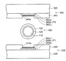
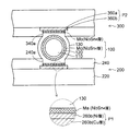
図5は実施形態の導電性ボールを示す図、図6は実施形態の導電性ボールの製造方法を示す図、図7〜図10は実施形態の電子装置を説明するための図である。
Claims (11)
- 銅ボールと、
前記銅ボールの外面を被覆するニッケル層と、
前記ニッケル層の外面を被覆する銅層と、
前記銅層の外面を被覆する錫系はんだと
を有し、
前記錫系はんだと前記銅層とを合計した重量に対する前記銅層の銅の重量が0.7wt%〜3wt%であることを特徴とする導電性ボール。 - 前記錫系はんだがリフロー加熱されて、前記錫系はんだに拡散する前記銅層の銅の濃度が0.7wt%〜3wt%であることを特徴とする請求項1に記載の導電性ボール。
- 前記錫系はんだは、錫/ビスマスはんだ、錫/銀はんだ、及び錫/ビスマス/ニッケルはんだのいずれかであることを特徴とする請求項1又は2に記載の導電性ボール。
- 第1接続パッドを備えた下側電子部材と、
前記下側電子部材の上に配置され、第2接続パッドを備えた上側電子部材と、
前記下側電子部材の第1接続パッドと前記上側電子部材の第2接続パッドとを接続する導電性ボールと
を有し、
前記導電性ボールは、
銅ボールと、
前記銅ボールの外面を被覆するニッケル層と、
前記銅層の外面を被覆する錫系はんだと
を有し、
前記ニッケル層と前記錫系はんだとの間に(Cu,Ni)6Sn5層が形成されていることを特徴とする電子装置。 - 前記第1接続パッド及び前記第2接続パッドの各表面はニッケル層又は銅層であり、
前記第1接続パッドと前記錫系はんだとの間、及び前記第2接続パッドと前記錫系はんだとの間に、(Cu,Ni)6Sn5層がそれぞれ形成されていることを特徴とする請求項4に記載の電子装置。 - 前記錫系はんだは、錫/ビスマスはんだ、錫/銀はんだ、及び錫/ビスマス/ニッケルはんだのいずれかであることを特徴とする請求項4又は5に記載の電子装置。
- 銅ボールを用意する工程と、
前記銅ボールの外面を被覆するニッケル層を形成する工程と、
前記ニッケル層の外面を被覆する銅層を形成する工程と、
前記銅層の外面を被覆する錫系はんだを形成する工程と
を有し、
前記錫系はんだがリフロー加熱される際に、前記銅層の銅が前記錫系はんだに拡散して、前記錫系はんだ内の銅の濃度が0.7wt%〜3wt%になるように、前記銅層の厚みが調整されることを特徴とする導電性ボールの製造方法。 - 第1接続パッドを備えた下側電子部材と、
第2接続パッドを備えた上側電子部材と、
銅ボールと、前記銅ボールの外面を被覆するニッケル層と、前記ニッケル層の外面を被覆する銅層と、前記銅層の外面を被覆する錫系はんだとを有する導電性ボールと
を用意する工程と、
前記下側電子部材の第1接続パッドと前記上側電子部材の第2接続パッドとを、前記導電性ボールの錫系はんだをリフロー加熱して接続する工程と
を有し、
前記導電性ボールの前記ニッケル層と前記錫系はんだとの間に(Cu,Ni)6Sn5層が形成されることを特徴とする電子装置の製造方法。 - 前記導電性ボールを用意する工程において、
前記錫系はんだをリフロー加熱する際に、前記銅層の銅が前記錫系はんだに拡散して、前記錫系はんだ内の銅の濃度が0.7wt%〜3wt%になるように、前記銅層の厚みが調整されていることを特徴とする請求項8に記載の電子装置の製造方法。 - 前記下側電子部材の第1接続パッドと前記上側電子部材の第2接続パッドとを接続する工程において、
前記第1接続パッド及び前記第2接続パッドの各表面はニッケル層又は銅層であり、
前記第1接続パッドと前記錫系はんだとの間、及び前記第2接続パッドと前記錫系はんだとの間に、(Cu,Ni)6Sn5層がそれぞれ形成されることを特徴とする請求項8又は9に記載の電子装置の製造方法。 - 前記錫系はんだは、錫/ビスマスはんだ、錫/銀はんだ、及び錫/ビスマス/ニッケルはんだのいずれかであることを特徴とする請求項8乃至10のいずれか一項に記載の電子装置の製造方法。
Priority Applications (2)
| Application Number | Priority Date | Filing Date | Title |
|---|---|---|---|
| JP2017133267A JP7014535B2 (ja) | 2017-07-07 | 2017-07-07 | 導電性ボール及び電子装置とそれらの製造方法 |
| US16/023,500 US10446513B2 (en) | 2017-07-07 | 2018-06-29 | Conductive ball having a tin-based solder covering an outer surface of the copper ball |
Applications Claiming Priority (1)
| Application Number | Priority Date | Filing Date | Title |
|---|---|---|---|
| JP2017133267A JP7014535B2 (ja) | 2017-07-07 | 2017-07-07 | 導電性ボール及び電子装置とそれらの製造方法 |
Publications (3)
| Publication Number | Publication Date |
|---|---|
| JP2019013960A true JP2019013960A (ja) | 2019-01-31 |
| JP2019013960A5 JP2019013960A5 (ja) | 2020-04-09 |
| JP7014535B2 JP7014535B2 (ja) | 2022-02-01 |
Family
ID=64903406
Family Applications (1)
| Application Number | Title | Priority Date | Filing Date |
|---|---|---|---|
| JP2017133267A Active JP7014535B2 (ja) | 2017-07-07 | 2017-07-07 | 導電性ボール及び電子装置とそれらの製造方法 |
Country Status (2)
| Country | Link |
|---|---|
| US (1) | US10446513B2 (ja) |
| JP (1) | JP7014535B2 (ja) |
Cited By (1)
| Publication number | Priority date | Publication date | Assignee | Title |
|---|---|---|---|---|
| WO2024038665A1 (ja) * | 2022-08-16 | 2024-02-22 | 日立Astemo株式会社 | 電子装置、電子装置の製造方法 |
Families Citing this family (4)
| Publication number | Priority date | Publication date | Assignee | Title |
|---|---|---|---|---|
| JP7041477B2 (ja) * | 2017-07-05 | 2022-03-24 | 新光電気工業株式会社 | 導電性ボール及び電子装置とそれらの製造方法 |
| US11145614B2 (en) * | 2019-10-18 | 2021-10-12 | Taiwan Semiconductor Manufacturing Company, Ltd. | Semiconductor device and method of manufacture |
| KR102461313B1 (ko) * | 2020-05-19 | 2022-11-01 | 엠케이전자 주식회사 | 리버스 리플로우용 심재를 이용한 반도체 패키지 |
| US12313478B2 (en) * | 2021-10-01 | 2025-05-27 | Sensitronics, LLC | Low drift force sensor with capacitive capability |
Citations (5)
| Publication number | Priority date | Publication date | Assignee | Title |
|---|---|---|---|---|
| JP2007075856A (ja) * | 2005-09-14 | 2007-03-29 | Nippon Steel Materials Co Ltd | Cuコアボール |
| JP2010099736A (ja) * | 2008-09-25 | 2010-05-06 | Hitachi Metals Ltd | 耐落下衝撃特性に優れた接続端子用ボールおよび接続端子ならびに電子部品 |
| JP2013031864A (ja) * | 2011-08-01 | 2013-02-14 | Hitachi Metals Ltd | はんだボールおよびはんだボールを用いた半導体装置 |
| JP2015186826A (ja) * | 2015-06-05 | 2015-10-29 | 日立金属株式会社 | はんだボールおよび半導体装置 |
| JP2016106033A (ja) * | 2007-10-19 | 2016-06-16 | 株式会社日本スペリア社 | はんだ継手 |
Family Cites Families (2)
| Publication number | Priority date | Publication date | Assignee | Title |
|---|---|---|---|---|
| JP2015072996A (ja) | 2013-10-02 | 2015-04-16 | 新光電気工業株式会社 | 半導体装置 |
| TWI637465B (zh) * | 2017-06-03 | 2018-10-01 | Siliconware Precision Industries Co., Ltd. | 電子封裝件及其製法 |
-
2017
- 2017-07-07 JP JP2017133267A patent/JP7014535B2/ja active Active
-
2018
- 2018-06-29 US US16/023,500 patent/US10446513B2/en active Active
Patent Citations (5)
| Publication number | Priority date | Publication date | Assignee | Title |
|---|---|---|---|---|
| JP2007075856A (ja) * | 2005-09-14 | 2007-03-29 | Nippon Steel Materials Co Ltd | Cuコアボール |
| JP2016106033A (ja) * | 2007-10-19 | 2016-06-16 | 株式会社日本スペリア社 | はんだ継手 |
| JP2010099736A (ja) * | 2008-09-25 | 2010-05-06 | Hitachi Metals Ltd | 耐落下衝撃特性に優れた接続端子用ボールおよび接続端子ならびに電子部品 |
| JP2013031864A (ja) * | 2011-08-01 | 2013-02-14 | Hitachi Metals Ltd | はんだボールおよびはんだボールを用いた半導体装置 |
| JP2015186826A (ja) * | 2015-06-05 | 2015-10-29 | 日立金属株式会社 | はんだボールおよび半導体装置 |
Cited By (2)
| Publication number | Priority date | Publication date | Assignee | Title |
|---|---|---|---|---|
| WO2024038665A1 (ja) * | 2022-08-16 | 2024-02-22 | 日立Astemo株式会社 | 電子装置、電子装置の製造方法 |
| JP2024026932A (ja) * | 2022-08-16 | 2024-02-29 | 日立Astemo株式会社 | 電子装置、電子装置の製造方法 |
Also Published As
| Publication number | Publication date |
|---|---|
| JP7014535B2 (ja) | 2022-02-01 |
| US20190013286A1 (en) | 2019-01-10 |
| US10446513B2 (en) | 2019-10-15 |
Similar Documents
| Publication | Publication Date | Title |
|---|---|---|
| JP7014535B2 (ja) | 導電性ボール及び電子装置とそれらの製造方法 | |
| TWI353643B (en) | Dual metal stud bumping for flip chip applications | |
| JP6667765B2 (ja) | 電極接続方法及び電極接続構造 | |
| JP3829325B2 (ja) | 半導体素子およびその製造方法並びに半導体装置の製造方法 | |
| CN102810522B (zh) | 封装结构和方法 | |
| TWI390642B (zh) | 穩定之金凸塊焊料連接 | |
| JP7041477B2 (ja) | 導電性ボール及び電子装置とそれらの製造方法 | |
| TWI493672B (zh) | 半導體裝置、電子裝置及半導體裝置之製造方法 | |
| CN103855116B (zh) | 电子部件、包括它的电子装置及电子装置的制造方法 | |
| US9129884B2 (en) | Solder bump joining structure with low resistance joining member | |
| JP2010109032A (ja) | 半導体装置の製造方法 | |
| JP2009239278A (ja) | 電子部品搭載用基板、及び、その製造方法 | |
| JPWO2013038594A1 (ja) | 実装構造およびその製造方法 | |
| TW201505492A (zh) | 印刷電路板及其製造方法 | |
| TWI473221B (zh) | 封裝基板及其製法 | |
| TW545098B (en) | Fine pad pitch organic circuit board with plating solder and method for fabricating the same | |
| JP2003133474A (ja) | 電子装置の実装構造 | |
| TWI313911B (en) | Conductive structure of package substrate and manufacturing method thereof | |
| JP4562314B2 (ja) | 電子装置の実装構造 | |
| JP2008028069A (ja) | 外部接合電極付き基板およびその製造方法 | |
| JP2002261115A (ja) | 電子装置の実装構造 | |
| JP2004056020A (ja) | 電極構造および電極構造を形成する方法 | |
| TW202449921A (zh) | 接合組件的形成方法 | |
| JP2002353368A (ja) | 電子装置の実装構造 | |
| KR101167815B1 (ko) | 반도체 패키지 구조 및 이의 제조 방법 |
Legal Events
| Date | Code | Title | Description |
|---|---|---|---|
| RD03 | Notification of appointment of power of attorney |
Free format text: JAPANESE INTERMEDIATE CODE: A7423 Effective date: 20180320 |
|
| A521 | Request for written amendment filed |
Free format text: JAPANESE INTERMEDIATE CODE: A523 Effective date: 20200227 |
|
| A621 | Written request for application examination |
Free format text: JAPANESE INTERMEDIATE CODE: A621 Effective date: 20200227 |
|
| A977 | Report on retrieval |
Free format text: JAPANESE INTERMEDIATE CODE: A971007 Effective date: 20210224 |
|
| A131 | Notification of reasons for refusal |
Free format text: JAPANESE INTERMEDIATE CODE: A131 Effective date: 20210309 |
|
| A521 | Request for written amendment filed |
Free format text: JAPANESE INTERMEDIATE CODE: A523 Effective date: 20210427 |
|
| A131 | Notification of reasons for refusal |
Free format text: JAPANESE INTERMEDIATE CODE: A131 Effective date: 20210803 |
|
| A521 | Request for written amendment filed |
Free format text: JAPANESE INTERMEDIATE CODE: A523 Effective date: 20210906 |
|
| TRDD | Decision of grant or rejection written | ||
| A01 | Written decision to grant a patent or to grant a registration (utility model) |
Free format text: JAPANESE INTERMEDIATE CODE: A01 Effective date: 20220111 |
|
| A61 | First payment of annual fees (during grant procedure) |
Free format text: JAPANESE INTERMEDIATE CODE: A61 Effective date: 20220120 |
|
| R150 | Certificate of patent or registration of utility model |
Ref document number: 7014535 Country of ref document: JP Free format text: JAPANESE INTERMEDIATE CODE: R150 |