JP2019197128A - 表示装置 - Google Patents
表示装置 Download PDFInfo
- Publication number
- JP2019197128A JP2019197128A JP2018090455A JP2018090455A JP2019197128A JP 2019197128 A JP2019197128 A JP 2019197128A JP 2018090455 A JP2018090455 A JP 2018090455A JP 2018090455 A JP2018090455 A JP 2018090455A JP 2019197128 A JP2019197128 A JP 2019197128A
- Authority
- JP
- Japan
- Prior art keywords
- transistor
- electrode
- control electrode
- wiring
- display device
- Prior art date
- Legal status (The legal status is an assumption and is not a legal conclusion. Google has not performed a legal analysis and makes no representation as to the accuracy of the status listed.)
- Pending
Links
Images


Classifications
-
- G—PHYSICS
- G02—OPTICS
- G02F—OPTICAL DEVICES OR ARRANGEMENTS FOR THE CONTROL OF LIGHT BY MODIFICATION OF THE OPTICAL PROPERTIES OF THE MEDIA OF THE ELEMENTS INVOLVED THEREIN; NON-LINEAR OPTICS; FREQUENCY-CHANGING OF LIGHT; OPTICAL LOGIC ELEMENTS; OPTICAL ANALOGUE/DIGITAL CONVERTERS
- G02F1/00—Devices or arrangements for the control of the intensity, colour, phase, polarisation or direction of light arriving from an independent light source, e.g. switching, gating or modulating; Non-linear optics
- G02F1/01—Devices or arrangements for the control of the intensity, colour, phase, polarisation or direction of light arriving from an independent light source, e.g. switching, gating or modulating; Non-linear optics for the control of the intensity, phase, polarisation or colour
- G02F1/13—Devices or arrangements for the control of the intensity, colour, phase, polarisation or direction of light arriving from an independent light source, e.g. switching, gating or modulating; Non-linear optics for the control of the intensity, phase, polarisation or colour based on liquid crystals, e.g. single liquid crystal display cells
- G02F1/133—Constructional arrangements; Operation of liquid crystal cells; Circuit arrangements
- G02F1/136—Liquid crystal cells structurally associated with a semi-conducting layer or substrate, e.g. cells forming part of an integrated circuit
- G02F1/1362—Active matrix addressed cells
- G02F1/136204—Arrangements to prevent high voltage or static electricity failures
-
- G—PHYSICS
- G02—OPTICS
- G02F—OPTICAL DEVICES OR ARRANGEMENTS FOR THE CONTROL OF LIGHT BY MODIFICATION OF THE OPTICAL PROPERTIES OF THE MEDIA OF THE ELEMENTS INVOLVED THEREIN; NON-LINEAR OPTICS; FREQUENCY-CHANGING OF LIGHT; OPTICAL LOGIC ELEMENTS; OPTICAL ANALOGUE/DIGITAL CONVERTERS
- G02F1/00—Devices or arrangements for the control of the intensity, colour, phase, polarisation or direction of light arriving from an independent light source, e.g. switching, gating or modulating; Non-linear optics
- G02F1/01—Devices or arrangements for the control of the intensity, colour, phase, polarisation or direction of light arriving from an independent light source, e.g. switching, gating or modulating; Non-linear optics for the control of the intensity, phase, polarisation or colour
- G02F1/13—Devices or arrangements for the control of the intensity, colour, phase, polarisation or direction of light arriving from an independent light source, e.g. switching, gating or modulating; Non-linear optics for the control of the intensity, phase, polarisation or colour based on liquid crystals, e.g. single liquid crystal display cells
- G02F1/133—Constructional arrangements; Operation of liquid crystal cells; Circuit arrangements
- G02F1/136—Liquid crystal cells structurally associated with a semi-conducting layer or substrate, e.g. cells forming part of an integrated circuit
- G02F1/1362—Active matrix addressed cells
- G02F1/136286—Wiring, e.g. gate line, drain line
-
- G—PHYSICS
- G02—OPTICS
- G02F—OPTICAL DEVICES OR ARRANGEMENTS FOR THE CONTROL OF LIGHT BY MODIFICATION OF THE OPTICAL PROPERTIES OF THE MEDIA OF THE ELEMENTS INVOLVED THEREIN; NON-LINEAR OPTICS; FREQUENCY-CHANGING OF LIGHT; OPTICAL LOGIC ELEMENTS; OPTICAL ANALOGUE/DIGITAL CONVERTERS
- G02F1/00—Devices or arrangements for the control of the intensity, colour, phase, polarisation or direction of light arriving from an independent light source, e.g. switching, gating or modulating; Non-linear optics
- G02F1/01—Devices or arrangements for the control of the intensity, colour, phase, polarisation or direction of light arriving from an independent light source, e.g. switching, gating or modulating; Non-linear optics for the control of the intensity, phase, polarisation or colour
- G02F1/13—Devices or arrangements for the control of the intensity, colour, phase, polarisation or direction of light arriving from an independent light source, e.g. switching, gating or modulating; Non-linear optics for the control of the intensity, phase, polarisation or colour based on liquid crystals, e.g. single liquid crystal display cells
- G02F1/133—Constructional arrangements; Operation of liquid crystal cells; Circuit arrangements
- G02F1/136—Liquid crystal cells structurally associated with a semi-conducting layer or substrate, e.g. cells forming part of an integrated circuit
- G02F1/1362—Active matrix addressed cells
- G02F1/1368—Active matrix addressed cells in which the switching element is a three-electrode device
-
- H—ELECTRICITY
- H10—SEMICONDUCTOR DEVICES; ELECTRIC SOLID-STATE DEVICES NOT OTHERWISE PROVIDED FOR
- H10D—INORGANIC ELECTRIC SEMICONDUCTOR DEVICES
- H10D30/00—Field-effect transistors [FET]
- H10D30/60—Insulated-gate field-effect transistors [IGFET]
- H10D30/67—Thin-film transistors [TFT]
- H10D30/674—Thin-film transistors [TFT] characterised by the active materials
- H10D30/6755—Oxide semiconductors, e.g. zinc oxide, copper aluminium oxide or cadmium stannate
-
- H—ELECTRICITY
- H10—SEMICONDUCTOR DEVICES; ELECTRIC SOLID-STATE DEVICES NOT OTHERWISE PROVIDED FOR
- H10D—INORGANIC ELECTRIC SEMICONDUCTOR DEVICES
- H10D86/00—Integrated devices formed in or on insulating or conducting substrates, e.g. formed in silicon-on-insulator [SOI] substrates or on stainless steel or glass substrates
- H10D86/40—Integrated devices formed in or on insulating or conducting substrates, e.g. formed in silicon-on-insulator [SOI] substrates or on stainless steel or glass substrates characterised by multiple TFTs
- H10D86/441—Interconnections, e.g. scanning lines
- H10D86/443—Interconnections, e.g. scanning lines adapted for preventing breakage, peeling or short circuiting
-
- H—ELECTRICITY
- H10—SEMICONDUCTOR DEVICES; ELECTRIC SOLID-STATE DEVICES NOT OTHERWISE PROVIDED FOR
- H10D—INORGANIC ELECTRIC SEMICONDUCTOR DEVICES
- H10D86/00—Integrated devices formed in or on insulating or conducting substrates, e.g. formed in silicon-on-insulator [SOI] substrates or on stainless steel or glass substrates
- H10D86/40—Integrated devices formed in or on insulating or conducting substrates, e.g. formed in silicon-on-insulator [SOI] substrates or on stainless steel or glass substrates characterised by multiple TFTs
- H10D86/481—Integrated devices formed in or on insulating or conducting substrates, e.g. formed in silicon-on-insulator [SOI] substrates or on stainless steel or glass substrates characterised by multiple TFTs integrated with passive devices, e.g. auxiliary capacitors
-
- H—ELECTRICITY
- H10—SEMICONDUCTOR DEVICES; ELECTRIC SOLID-STATE DEVICES NOT OTHERWISE PROVIDED FOR
- H10D—INORGANIC ELECTRIC SEMICONDUCTOR DEVICES
- H10D86/00—Integrated devices formed in or on insulating or conducting substrates, e.g. formed in silicon-on-insulator [SOI] substrates or on stainless steel or glass substrates
- H10D86/40—Integrated devices formed in or on insulating or conducting substrates, e.g. formed in silicon-on-insulator [SOI] substrates or on stainless steel or glass substrates characterised by multiple TFTs
- H10D86/60—Integrated devices formed in or on insulating or conducting substrates, e.g. formed in silicon-on-insulator [SOI] substrates or on stainless steel or glass substrates characterised by multiple TFTs wherein the TFTs are in active matrices
-
- H—ELECTRICITY
- H10—SEMICONDUCTOR DEVICES; ELECTRIC SOLID-STATE DEVICES NOT OTHERWISE PROVIDED FOR
- H10D—INORGANIC ELECTRIC SEMICONDUCTOR DEVICES
- H10D89/00—Aspects of integrated devices not covered by groups H10D84/00 - H10D88/00
- H10D89/60—Integrated devices comprising arrangements for electrical or thermal protection, e.g. protection circuits against electrostatic discharge [ESD]
- H10D89/601—Integrated devices comprising arrangements for electrical or thermal protection, e.g. protection circuits against electrostatic discharge [ESD] for devices having insulated gate electrodes, e.g. for IGFETs or IGBTs
- H10D89/811—Integrated devices comprising arrangements for electrical or thermal protection, e.g. protection circuits against electrostatic discharge [ESD] for devices having insulated gate electrodes, e.g. for IGFETs or IGBTs using FETs as protective elements
-
- G—PHYSICS
- G02—OPTICS
- G02F—OPTICAL DEVICES OR ARRANGEMENTS FOR THE CONTROL OF LIGHT BY MODIFICATION OF THE OPTICAL PROPERTIES OF THE MEDIA OF THE ELEMENTS INVOLVED THEREIN; NON-LINEAR OPTICS; FREQUENCY-CHANGING OF LIGHT; OPTICAL LOGIC ELEMENTS; OPTICAL ANALOGUE/DIGITAL CONVERTERS
- G02F2202/00—Materials and properties
- G02F2202/22—Antistatic materials or arrangements
-
- H—ELECTRICITY
- H10—SEMICONDUCTOR DEVICES; ELECTRIC SOLID-STATE DEVICES NOT OTHERWISE PROVIDED FOR
- H10D—INORGANIC ELECTRIC SEMICONDUCTOR DEVICES
- H10D89/00—Aspects of integrated devices not covered by groups H10D84/00 - H10D88/00
- H10D89/60—Integrated devices comprising arrangements for electrical or thermal protection, e.g. protection circuits against electrostatic discharge [ESD]
- H10D89/601—Integrated devices comprising arrangements for electrical or thermal protection, e.g. protection circuits against electrostatic discharge [ESD] for devices having insulated gate electrodes, e.g. for IGFETs or IGBTs
- H10D89/911—Integrated devices comprising arrangements for electrical or thermal protection, e.g. protection circuits against electrostatic discharge [ESD] for devices having insulated gate electrodes, e.g. for IGFETs or IGBTs using passive elements as protective elements
-
- H—ELECTRICITY
- H10—SEMICONDUCTOR DEVICES; ELECTRIC SOLID-STATE DEVICES NOT OTHERWISE PROVIDED FOR
- H10D—INORGANIC ELECTRIC SEMICONDUCTOR DEVICES
- H10D89/00—Aspects of integrated devices not covered by groups H10D84/00 - H10D88/00
- H10D89/60—Integrated devices comprising arrangements for electrical or thermal protection, e.g. protection circuits against electrostatic discharge [ESD]
- H10D89/601—Integrated devices comprising arrangements for electrical or thermal protection, e.g. protection circuits against electrostatic discharge [ESD] for devices having insulated gate electrodes, e.g. for IGFETs or IGBTs
- H10D89/931—Integrated devices comprising arrangements for electrical or thermal protection, e.g. protection circuits against electrostatic discharge [ESD] for devices having insulated gate electrodes, e.g. for IGFETs or IGBTs characterised by the dispositions of the protective arrangements
Landscapes
- Physics & Mathematics (AREA)
- Nonlinear Science (AREA)
- Engineering & Computer Science (AREA)
- Microelectronics & Electronic Packaging (AREA)
- Mathematical Physics (AREA)
- Chemical & Material Sciences (AREA)
- Crystallography & Structural Chemistry (AREA)
- General Physics & Mathematics (AREA)
- Optics & Photonics (AREA)
- Liquid Crystal (AREA)
- Devices For Indicating Variable Information By Combining Individual Elements (AREA)
Abstract
Description
<液晶表示装置の構成>
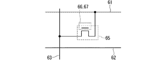
図1は、本発明に係る実施の形態1の液晶表示装置100の全体構成を模式的に示す平面図である。

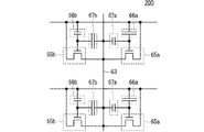
図9は、本発明の実施の形態2に係る液晶表示装置200に設けられた静電気防止回路を示す等価回路図である。なお、液晶表示装置200の全体構成は、図1に示した液晶表示装置100の全体構成と同様である。
図6〜図8に示したMOSトランジスタT1においては、チャネルエッチ型のTFTを例示したが、静電気防止回路を構成するTFTとしてはチャネルエッチ型に限定されるものではなく、エッチストッパ型、トップゲート型などでも使用可能であり、ドレイン電極とソース電極が、フローティングのゲート電極との間で静電容量を形成する構成であれば使用可能である。
Claims (8)
- 走査配線および信号配線が互いに交差するように配置され、隣接する前記走査配線と前記信号配線とで囲まれる領域に設けられた画素がマトリクス状に配列された表示領域と、該表示領域に接する非表示領域とを備えた表示装置であって、
前記表示装置は、
前記非表示領域に設けられた共通電位が与えられる共通配線と、前記非表示領域における前記信号配線および前記走査配線の少なくとも一方との間に設けられた静電気防止回路を備え、
前記静電気防止回路は、
制御電極がフローティング状態であって、
第1の主電極が前記信号配線または前記走査配線に接続され、
第2の主電極が前記共通配線に接続された第1のトランジスタを少なくとも有し、
前記第1のトランジスタは、
前記制御電極と前記信号配線または前記走査配線との間に形成される第1の静電容量が、前記制御電極と前記共通配線との間に形成される第2の静電容量よりも大きくなるように形成される、表示装置。 - 前記静電気防止回路は、
制御電極がフローティング状態であって、
第1の主電極が前記信号配線または前記走査配線に接続され、
第2の主電極が前記共通配線に接続された第2のトランジスタをさらに有し、
前記第2のトランジスタは、
前記制御電極と前記共通配線との間に形成される第2の静電容量が、前記制御電極と前記信号配線または前記走査配線との間に形成される第1の静電容量よりも大きくなるように形成される、請求項1記載の表示装置。 - 前記第1のトランジスタにおける、前記第1および第2の静電容量の大小関係は、
前記制御電極と前記第1の主電極との平面方向での重なり面積が、
前記制御電極と前記第2の主電極との平面方向での重なり面積より大きくなるように、前記第1および第2の主電極の面積を設定することで規定される、請求項1記載の表示装置。 - 前記第1のトランジスタにおける、前記第1および第2の静電容量の大小関係は、
前記第1のトランジスタの前記制御電極と前記第1の主電極との平面方向での重なり面積が、
前記第1のトランジスタの前記制御電極と前記第2の主電極との平面方向での重なり面積より大きくなるように、前記第1および第2の主電極の面積を設定することで規定され、
前記第2のトランジスタにおける、前記第1および第2の静電容量の大小関係は、
前記第2のトランジスタ前記制御電極と前記第2の主電極との平面方向での重なり面積が、
前記第2のトランジスタの前記制御電極と前記第1の主電極との平面方向視での重なり面積より大きくなるように、前記第1および第2の主電極の面積を設定することで規定される、請求項2記載の表示装置。 - 前記第1のトランジスタにおける、前記第1および第2の静電容量の大小関係は、
前記第1のトランジスタの前記制御電極と前記第1の主電極との垂直方向での離間距離が、
前記第1のトランジスタの前記制御電極と前記第2の主電極との垂直方向での離間距離より短くなるように、前記制御電極から前記第1および第2の主電極までの垂直方向の距離を設定することで規定される、請求項1記載の表示装置。 - 前記第1のトランジスタにおける、前記第1および第2の静電容量の大小関係は、
前記第1のトランジスタの前記制御電極と前記第1の主電極との垂直方向での離間距離が、
前記第1のトランジスタの前記制御電極と前記第2の主電極との垂直方向での離間距離より短くなるように、前記制御電極から前記第1および第2の主電極までの垂直方向の距離を設定することで規定され、
前記第2のトランジスタにおける、前記第1および第2の静電容量の大小関係は、
前記第2のトランジスタの前記制御電極と前記第2の主電極との垂直方向での離間距離が、
前記第2のトランジスタの前記制御電極と前記第1の主電極との垂直方向での離間距離より短くなるように、前記制御電極から前記第1および第2の主電極までの垂直方向の距離を設定することで規定される、請求項2記載の表示装置。 - 前記第1のトランジスタは、
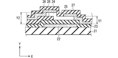
前記制御電極とゲート絶縁膜を間に挟んで設けられたチャネル層を備え、
前記チャネル層は、酸化物半導体で構成される、請求項1記載の表示装置。 - 前記第1のトランジスタは、
前記第1のトランジスタの前記制御電極とゲート絶縁膜を間に挟んで設けられたチャネル層を備え、
前記第1のトランジスタの前記チャネル層は、酸化物半導体で構成され、
前記第2のトランジスタは、
前記第2のトランジスタの前記制御電極とゲート絶縁膜を間に挟んで設けられたチャネル層を備え、
前記第2のトランジスタの前記チャネル層は、酸化物半導体で構成される、請求項2記載の表示装置。
Priority Applications (3)
| Application Number | Priority Date | Filing Date | Title |
|---|---|---|---|
| JP2018090455A JP2019197128A (ja) | 2018-05-09 | 2018-05-09 | 表示装置 |
| US16/396,951 US11231628B2 (en) | 2018-05-09 | 2019-04-29 | Display |
| CN201910364802.3A CN110471227A (zh) | 2018-05-09 | 2019-04-30 | 显示装置 |
Applications Claiming Priority (1)
| Application Number | Priority Date | Filing Date | Title |
|---|---|---|---|
| JP2018090455A JP2019197128A (ja) | 2018-05-09 | 2018-05-09 | 表示装置 |
Publications (2)
| Publication Number | Publication Date |
|---|---|
| JP2019197128A true JP2019197128A (ja) | 2019-11-14 |
| JP2019197128A5 JP2019197128A5 (ja) | 2021-05-27 |
Family
ID=68464592
Family Applications (1)
| Application Number | Title | Priority Date | Filing Date |
|---|---|---|---|
| JP2018090455A Pending JP2019197128A (ja) | 2018-05-09 | 2018-05-09 | 表示装置 |
Country Status (3)
| Country | Link |
|---|---|
| US (1) | US11231628B2 (ja) |
| JP (1) | JP2019197128A (ja) |
| CN (1) | CN110471227A (ja) |
Families Citing this family (2)
| Publication number | Priority date | Publication date | Assignee | Title |
|---|---|---|---|---|
| CN208336227U (zh) * | 2018-07-20 | 2019-01-04 | 京东方科技集团股份有限公司 | 静电保护电路、阵列基板及显示装置 |
| CN117954442A (zh) * | 2022-10-31 | 2024-04-30 | 群创光电股份有限公司 | 调变装置 |
Citations (3)
| Publication number | Priority date | Publication date | Assignee | Title |
|---|---|---|---|---|
| US6175394B1 (en) * | 1996-12-03 | 2001-01-16 | Chung-Cheng Wu | Capacitively coupled field effect transistors for electrostatic discharge protection in flat panel displays |
| JP2010092036A (ja) * | 2008-09-12 | 2010-04-22 | Semiconductor Energy Lab Co Ltd | 表示装置 |
| JP2012256838A (ja) * | 2011-02-02 | 2012-12-27 | Semiconductor Energy Lab Co Ltd | 半導体装置 |
Family Cites Families (10)
| Publication number | Priority date | Publication date | Assignee | Title |
|---|---|---|---|---|
| JPS6179259A (ja) | 1984-09-26 | 1986-04-22 | Seiko Instr & Electronics Ltd | 薄膜トランジスタ装置 |
| JPH08262485A (ja) | 1995-03-20 | 1996-10-11 | Nec Corp | 液晶表示装置 |
| KR100239424B1 (ko) | 1997-09-26 | 2000-01-15 | 김영환 | 정전기 보호회로 |
| TW457690B (en) | 1999-08-31 | 2001-10-01 | Fujitsu Ltd | Liquid crystal display |
| JP4410912B2 (ja) | 2000-06-07 | 2010-02-10 | Nec液晶テクノロジー株式会社 | 静電保護回路 |
| JP4385691B2 (ja) | 2003-09-12 | 2009-12-16 | カシオ計算機株式会社 | 表示パネルの静電気保護構造及び液晶表示パネル |
| KR20150040873A (ko) * | 2012-08-03 | 2015-04-15 | 가부시키가이샤 한도오따이 에네루기 켄큐쇼 | 반도체 장치 |
| CN103944154A (zh) | 2013-12-11 | 2014-07-23 | 厦门天马微电子有限公司 | 一种静电保护电路及液晶显示器 |
| CN107408580B (zh) | 2015-04-28 | 2020-10-27 | 三菱电机株式会社 | 晶体管、薄膜晶体管基板以及液晶显示装置 |
| CN105487317B (zh) | 2016-01-25 | 2019-04-02 | 京东方科技集团股份有限公司 | 一种基板及显示装置 |
-
2018
- 2018-05-09 JP JP2018090455A patent/JP2019197128A/ja active Pending
-
2019
- 2019-04-29 US US16/396,951 patent/US11231628B2/en active Active
- 2019-04-30 CN CN201910364802.3A patent/CN110471227A/zh active Pending
Patent Citations (3)
| Publication number | Priority date | Publication date | Assignee | Title |
|---|---|---|---|---|
| US6175394B1 (en) * | 1996-12-03 | 2001-01-16 | Chung-Cheng Wu | Capacitively coupled field effect transistors for electrostatic discharge protection in flat panel displays |
| JP2010092036A (ja) * | 2008-09-12 | 2010-04-22 | Semiconductor Energy Lab Co Ltd | 表示装置 |
| JP2012256838A (ja) * | 2011-02-02 | 2012-12-27 | Semiconductor Energy Lab Co Ltd | 半導体装置 |
Also Published As
| Publication number | Publication date |
|---|---|
| US11231628B2 (en) | 2022-01-25 |
| US20190346726A1 (en) | 2019-11-14 |
| CN110471227A (zh) | 2019-11-19 |
Similar Documents
| Publication | Publication Date | Title |
|---|---|---|
| CN102844803B (zh) | 有源矩阵基板和显示装置 | |
| US20130148049A1 (en) | Display device | |
| TW201435704A (zh) | 內建觸控面板型顯示裝置 | |
| CN110045881B (zh) | 触控显示面板 | |
| CN104238224B (zh) | 显示面板及其制造方法 | |
| US10481427B2 (en) | Array substrate, manufacturing method, display panel and electronic device | |
| US9146432B2 (en) | Electro-optic device having an electrostatic protection circuit for protecting a gate driver and display device thereof | |
| WO2019233113A1 (zh) | 阵列基板及显示装置 | |
| TWI399603B (zh) | 液晶顯示裝置 | |
| JP4065645B2 (ja) | アクティブマトリクス型液晶表示装置 | |
| US20190221590A1 (en) | Active matrix substrate and display device provided with active matrix substrate | |
| JP2019197128A (ja) | 表示装置 | |
| US9703152B2 (en) | Liquid crystal display device | |
| US20210063830A1 (en) | Electro-optical device and electronic apparatus | |
| US20240142834A1 (en) | Electro-optical device and electronic apparatus | |
| JP4905136B2 (ja) | 液晶装置 | |
| JP5481790B2 (ja) | 電気光学装置 | |
| JP5127234B2 (ja) | 半導体装置、電気光学装置並びに電子機器 | |
| US20250284164A1 (en) | Electro-optical device and electronic apparatus | |
| US12339548B2 (en) | Electro-optical device and electronic device | |
| US20260063957A1 (en) | Electro-optical device and electronic instrument | |
| US20250284165A1 (en) | Electro-optical device and electronic apparatus | |
| US20260068321A1 (en) | Electro-optical device and electronic instrument | |
| US11500251B2 (en) | Electro-optical device and electronic apparatus | |
| CN111694196A (zh) | 电光装置以及电子设备 |
Legal Events
| Date | Code | Title | Description |
|---|---|---|---|
| A521 | Request for written amendment filed |
Free format text: JAPANESE INTERMEDIATE CODE: A523 Effective date: 20210416 |
|
| A621 | Written request for application examination |
Free format text: JAPANESE INTERMEDIATE CODE: A621 Effective date: 20210416 |
|
| A711 | Notification of change in applicant |
Free format text: JAPANESE INTERMEDIATE CODE: A711 Effective date: 20211115 |
|
| A977 | Report on retrieval |
Free format text: JAPANESE INTERMEDIATE CODE: A971007 Effective date: 20220215 |
|
| A131 | Notification of reasons for refusal |
Free format text: JAPANESE INTERMEDIATE CODE: A131 Effective date: 20220308 |
|
| A02 | Decision of refusal |
Free format text: JAPANESE INTERMEDIATE CODE: A02 Effective date: 20221011 |