JP3860582B2 - 半導体装置の製造方法 - Google Patents
半導体装置の製造方法 Download PDFInfo
- Publication number
- JP3860582B2 JP3860582B2 JP2004111095A JP2004111095A JP3860582B2 JP 3860582 B2 JP3860582 B2 JP 3860582B2 JP 2004111095 A JP2004111095 A JP 2004111095A JP 2004111095 A JP2004111095 A JP 2004111095A JP 3860582 B2 JP3860582 B2 JP 3860582B2
- Authority
- JP
- Japan
- Prior art keywords
- insulating film
- fin
- layer
- type
- gate electrode
- Prior art date
- Legal status (The legal status is an assumption and is not a legal conclusion. Google has not performed a legal analysis and makes no representation as to the accuracy of the status listed.)
- Expired - Fee Related
Links
Images








Classifications
-
- H—ELECTRICITY
- H10—SEMICONDUCTOR DEVICES; ELECTRIC SOLID-STATE DEVICES NOT OTHERWISE PROVIDED FOR
- H10D—INORGANIC ELECTRIC SEMICONDUCTOR DEVICES
- H10D30/00—Field-effect transistors [FET]
- H10D30/60—Insulated-gate field-effect transistors [IGFET]
- H10D30/62—Fin field-effect transistors [FinFET]
-
- H—ELECTRICITY
- H10—SEMICONDUCTOR DEVICES; ELECTRIC SOLID-STATE DEVICES NOT OTHERWISE PROVIDED FOR
- H10B—ELECTRONIC MEMORY DEVICES
- H10B10/00—Static random access memory [SRAM] devices
-
- H—ELECTRICITY
- H10—SEMICONDUCTOR DEVICES; ELECTRIC SOLID-STATE DEVICES NOT OTHERWISE PROVIDED FOR
- H10B—ELECTRONIC MEMORY DEVICES
- H10B10/00—Static random access memory [SRAM] devices
- H10B10/12—Static random access memory [SRAM] devices comprising a MOSFET load element
- H10B10/125—Static random access memory [SRAM] devices comprising a MOSFET load element the MOSFET being a thin film transistor [TFT]
-
- H—ELECTRICITY
- H10—SEMICONDUCTOR DEVICES; ELECTRIC SOLID-STATE DEVICES NOT OTHERWISE PROVIDED FOR
- H10D—INORGANIC ELECTRIC SEMICONDUCTOR DEVICES
- H10D30/00—Field-effect transistors [FET]
- H10D30/01—Manufacture or treatment
- H10D30/021—Manufacture or treatment of FETs having insulated gates [IGFET]
- H10D30/024—Manufacture or treatment of FETs having insulated gates [IGFET] of fin field-effect transistors [FinFET]
-
- H—ELECTRICITY
- H10—SEMICONDUCTOR DEVICES; ELECTRIC SOLID-STATE DEVICES NOT OTHERWISE PROVIDED FOR
- H10D—INORGANIC ELECTRIC SEMICONDUCTOR DEVICES
- H10D86/00—Integrated devices formed in or on insulating or conducting substrates, e.g. formed in silicon-on-insulator [SOI] substrates or on stainless steel or glass substrates
- H10D86/01—Manufacture or treatment
- H10D86/011—Manufacture or treatment comprising FinFETs
-
- H—ELECTRICITY
- H10—SEMICONDUCTOR DEVICES; ELECTRIC SOLID-STATE DEVICES NOT OTHERWISE PROVIDED FOR
- H10D—INORGANIC ELECTRIC SEMICONDUCTOR DEVICES
- H10D86/00—Integrated devices formed in or on insulating or conducting substrates, e.g. formed in silicon-on-insulator [SOI] substrates or on stainless steel or glass substrates
- H10D86/201—Integrated devices formed in or on insulating or conducting substrates, e.g. formed in silicon-on-insulator [SOI] substrates or on stainless steel or glass substrates the substrates comprising an insulating layer on a semiconductor body, e.g. SOI
- H10D86/215—Integrated devices formed in or on insulating or conducting substrates, e.g. formed in silicon-on-insulator [SOI] substrates or on stainless steel or glass substrates the substrates comprising an insulating layer on a semiconductor body, e.g. SOI comprising FinFETs
-
- H—ELECTRICITY
- H10—SEMICONDUCTOR DEVICES; ELECTRIC SOLID-STATE DEVICES NOT OTHERWISE PROVIDED FOR
- H10D—INORGANIC ELECTRIC SEMICONDUCTOR DEVICES
- H10D89/00—Aspects of integrated devices not covered by groups H10D84/00 - H10D88/00
- H10D89/10—Integrated device layouts
Landscapes
- Semiconductor Memories (AREA)
- Thin Film Transistor (AREA)
- Metal-Oxide And Bipolar Metal-Oxide Semiconductor Integrated Circuits (AREA)
Description
E.J.Nowak,et al."A Functional FinFET−DGCMOS SRAM Cell" International Electron Device Meeting 2002,P.411〜P.414
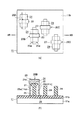
図1および図2(a),(b)は、本発明の第1の実施形態にしたがった、立体構造を有するMOSトランジスタの構成例を示すものである。なお、ここでは、6つのトランジスタからなるSRAM(Static Random Access Memory)セルを構成する場合を例に説明する。また、図1は斜視図、図2(a)は平面図であり、図2(b)は図2(a)のIIB−IIB線に沿う断面図である。
図8は、本発明の第2の実施形態にしたがった、6つのトランジスタにより構成されるSRAMセルの一例を示すものである。ここでは、第1の実施形態に示した4つのT字形状を有する絶縁膜層と2つの半導体膜(Si−フィン)とを備える突起部を用いて、1つのSRAMセルを構成する場合について説明する。
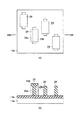
図24(a),(b)〜図27(a),(b)は、本発明の第3の実施形態にしたがった、突起部の他の構成例を示すものである。ここでは、上記した2つのSi−フィンと1つの絶縁膜層とからなる突起部の製造に、Si製のバルク(bulk)基板を用いるようにした場合について説明する。
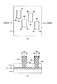
図28(a),(b)〜図33(a),(b)は、本発明の第4の実施形態にしたがった、突起部のさらに別の構成例を示すものである。ここでは、上記した2つのSi−フィンと1つの絶縁膜層とからなる突起部を、エピタキシャル技術を用いて製造するようにした場合について説明する。
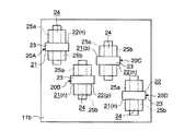
図34は、本発明の第5の実施形態にしたがった、6つのトランジスタにより構成されるSRAMセルの他の例を示すものである。ここでは、2つの突起部を用いて、1つのSRAMセルを構成する場合について説明する。
Claims (5)
- 基板上に、半導体層を介して第1の絶縁膜を堆積する工程と、
前記第1の絶縁膜および前記半導体層を選択的にエッチングして、長方形状の平面を有する開口部を形成する工程と、
前記第1の絶縁膜を選択的にエッチングして、第1および第2の半導体膜の幅に応じたプルバック部を形成する工程と、
前記開口部および前記プルバック部を第2の絶縁膜により埋め込んで、T字形状の断面を有する絶縁膜層を形成する工程と、
前記第1の絶縁膜をすべて除去した後、前記絶縁膜層をマスクに前記半導体層をエッチングし、前記絶縁膜層の第1および第2の側面に、ゲート長よりも幅の細い前記第1および第2の半導体膜を形成する工程と、
前記絶縁膜層および前記第1および第2の半導体膜を、それぞれ上部より挟み込むようにしてゲート電極を形成する工程と
を具備したことを特徴とする半導体装置の製造方法。 - 前記プルバック部は、前記開口部の長手方向の各側面に対応する、前記第1の絶縁膜を後退させることによって形成されることを特徴とする請求項1に記載の半導体装置の製造方法。
- 前記絶縁膜層を形成した後、その長手方向の両端部を除く、前記絶縁膜層上にレジスト膜を形成し、前記レジスト膜をマスクに、前記第2の絶縁膜を選択的にエッチングする工程をさらに備えることを特徴とする請求項1に記載の半導体装置の製造方法。
- 前記レジスト膜は、前記第2の絶縁膜を選択的にエッチングするために、前記プルバック部よりも長い非マスク領域を有して形成されることを特徴とする請求項3に記載の半導体装置の製造方法。
- 前記第2の絶縁膜は、前記第1の絶縁膜の膜厚分だけエッチングされることを特徴とする請求項3に記載の半導体装置の製造方法。
Priority Applications (4)
| Application Number | Priority Date | Filing Date | Title |
|---|---|---|---|
| JP2004111095A JP3860582B2 (ja) | 2003-07-31 | 2004-04-05 | 半導体装置の製造方法 |
| US10/835,122 US7164175B2 (en) | 2003-07-31 | 2004-04-28 | Semiconductor device with silicon-film fins and method of manufacturing the same |
| TW093120942A TWI277200B (en) | 2003-07-31 | 2004-07-14 | Semiconductor device and manufacturing method thereof |
| US11/637,734 US7541245B2 (en) | 2003-07-31 | 2006-12-12 | Semiconductor device with silicon-film fins and method of manufacturing the same |
Applications Claiming Priority (2)
| Application Number | Priority Date | Filing Date | Title |
|---|---|---|---|
| JP2003204386 | 2003-07-31 | ||
| JP2004111095A JP3860582B2 (ja) | 2003-07-31 | 2004-04-05 | 半導体装置の製造方法 |
Publications (2)
| Publication Number | Publication Date |
|---|---|
| JP2005064459A JP2005064459A (ja) | 2005-03-10 |
| JP3860582B2 true JP3860582B2 (ja) | 2006-12-20 |
Family
ID=34106869
Family Applications (1)
| Application Number | Title | Priority Date | Filing Date |
|---|---|---|---|
| JP2004111095A Expired - Fee Related JP3860582B2 (ja) | 2003-07-31 | 2004-04-05 | 半導体装置の製造方法 |
Country Status (3)
| Country | Link |
|---|---|
| US (2) | US7164175B2 (ja) |
| JP (1) | JP3860582B2 (ja) |
| TW (1) | TWI277200B (ja) |
Families Citing this family (25)
| Publication number | Priority date | Publication date | Assignee | Title |
|---|---|---|---|---|
| DE10220923B4 (de) * | 2002-05-10 | 2006-10-26 | Infineon Technologies Ag | Verfahren zur Herstellung eines nicht-flüchtigen Flash-Halbleiterspeichers |
| US7018551B2 (en) * | 2003-12-09 | 2006-03-28 | International Business Machines Corporation | Pull-back method of forming fins in FinFets |
| WO2005119763A1 (ja) * | 2004-06-04 | 2005-12-15 | Nec Corporation | 半導体装置およびその製造方法 |
| US7388663B2 (en) * | 2004-10-28 | 2008-06-17 | Asml Netherlands B.V. | Optical position assessment apparatus and method |
| JP2006128494A (ja) * | 2004-10-29 | 2006-05-18 | Toshiba Corp | 半導体集積回路装置及びその製造方法 |
| JP4648096B2 (ja) * | 2005-06-03 | 2011-03-09 | 株式会社東芝 | 半導体装置の製造方法 |
| WO2007049170A1 (en) * | 2005-10-25 | 2007-05-03 | Nxp B.V. | Finfet transistors |
| US7547947B2 (en) * | 2005-11-15 | 2009-06-16 | International Business Machines Corporation | SRAM cell |
| JP2007173326A (ja) * | 2005-12-19 | 2007-07-05 | Korea Advanced Inst Of Sci Technol | シリコンフィンとシリコンボディとからなるチャネルを有する電界効果トランジスタおよびその製造方法 |
| KR100732304B1 (ko) * | 2006-03-23 | 2007-06-25 | 주식회사 하이닉스반도체 | 반도체 소자 및 그의 제조 방법 |
| JP5004251B2 (ja) | 2006-12-28 | 2012-08-22 | 独立行政法人産業技術総合研究所 | Sramセル及びsram装置 |
| JP4461154B2 (ja) * | 2007-05-15 | 2010-05-12 | 株式会社東芝 | 半導体装置 |
| US7923337B2 (en) * | 2007-06-20 | 2011-04-12 | International Business Machines Corporation | Fin field effect transistor devices with self-aligned source and drain regions |
| US20090001470A1 (en) * | 2007-06-26 | 2009-01-01 | Anderson Brent A | Method for forming acute-angle spacer for non-orthogonal finfet and the resulting structure |
| US20090124097A1 (en) * | 2007-11-09 | 2009-05-14 | International Business Machines Corporation | Method of forming narrow fins in finfet devices with reduced spacing therebetween |
| US8659088B2 (en) | 2008-03-28 | 2014-02-25 | National Institute Of Advanced Industrial Science And Technology | SRAM cell and SRAM device |
| US8582352B2 (en) * | 2011-12-06 | 2013-11-12 | Taiwan Semiconductor Manufacturing Company, Ltd. | Methods and apparatus for FinFET SRAM cells |
| US8693235B2 (en) | 2011-12-06 | 2014-04-08 | Taiwan Semiconductor Manufacturing Company, Ltd. | Methods and apparatus for finFET SRAM arrays in integrated circuits |
| KR102840942B1 (ko) * | 2011-12-22 | 2025-08-01 | 인텔 코포레이션 | 반도체 구조 |
| WO2013187119A1 (ja) * | 2012-06-14 | 2013-12-19 | コニカミノルタ株式会社 | 電界発光素子およびその電界発光素子を用いた照明装置 |
| WO2015045207A1 (ja) * | 2013-09-27 | 2015-04-02 | パナソニック株式会社 | 半導体集積回路および半導体集積回路装置 |
| US9136384B2 (en) * | 2013-12-05 | 2015-09-15 | Stmicroelectronics, Inc. | Method for the formation of a FinFET device having partially dielectric isolated Fin structure |
| KR102217246B1 (ko) * | 2014-11-12 | 2021-02-18 | 삼성전자주식회사 | 집적회로 소자 및 그 제조 방법 |
| CN106156375B (zh) * | 2015-03-24 | 2019-01-04 | 展讯通信(上海)有限公司 | 一种存储器编译器拼接方法和存储器 |
| US9466723B1 (en) * | 2015-06-26 | 2016-10-11 | Globalfoundries Inc. | Liner and cap layer for placeholder source/drain contact structure planarization and replacement |
Family Cites Families (13)
| Publication number | Priority date | Publication date | Assignee | Title |
|---|---|---|---|---|
| JPH03187272A (ja) | 1989-12-15 | 1991-08-15 | Mitsubishi Electric Corp | Mos型電界効果トランジスタ及びその製造方法 |
| JPH04250667A (ja) | 1991-01-28 | 1992-09-07 | Oki Electric Ind Co Ltd | 半導体装置及びその製造方法 |
| JP2789931B2 (ja) | 1991-05-27 | 1998-08-27 | 日本電気株式会社 | 半導体装置 |
| US5554870A (en) | 1994-02-04 | 1996-09-10 | Motorola, Inc. | Integrated circuit having both vertical and horizontal devices and process for making the same |
| EP0859330A1 (en) * | 1997-02-12 | 1998-08-19 | Kokusai Denshin Denwa Co., Ltd | Document retrieval apparatus |
| IL121181A0 (en) * | 1997-06-27 | 1997-11-20 | Agentics Ltd | A method and system for unifying multiple information resources into hierarchial integrated information resource accessible by means of user interface |
| US6073135A (en) * | 1998-03-10 | 2000-06-06 | Alta Vista Company | Connectivity server for locating linkage information between Web pages |
| US6112203A (en) * | 1998-04-09 | 2000-08-29 | Altavista Company | Method for ranking documents in a hyperlinked environment using connectivity and selective content analysis |
| JP4083869B2 (ja) | 1998-05-14 | 2008-04-30 | 宮城沖電気株式会社 | 半導体装置の製造方法 |
| US6675161B1 (en) * | 1999-05-04 | 2004-01-06 | Inktomi Corporation | Managing changes to a directory of electronic documents |
| US6381607B1 (en) * | 1999-06-19 | 2002-04-30 | Kent Ridge Digital Labs | System of organizing catalog data for searching and retrieval |
| US6868525B1 (en) * | 2000-02-01 | 2005-03-15 | Alberti Anemometer Llc | Computer graphic display visualization system and method |
| US6762448B1 (en) * | 2003-04-03 | 2004-07-13 | Advanced Micro Devices, Inc. | FinFET device with multiple fin structures |
-
2004
- 2004-04-05 JP JP2004111095A patent/JP3860582B2/ja not_active Expired - Fee Related
- 2004-04-28 US US10/835,122 patent/US7164175B2/en not_active Expired - Fee Related
- 2004-07-14 TW TW093120942A patent/TWI277200B/zh not_active IP Right Cessation
-
2006
- 2006-12-12 US US11/637,734 patent/US7541245B2/en not_active Expired - Lifetime
Also Published As
| Publication number | Publication date |
|---|---|
| US7164175B2 (en) | 2007-01-16 |
| TW200509374A (en) | 2005-03-01 |
| US20050026377A1 (en) | 2005-02-03 |
| US7541245B2 (en) | 2009-06-02 |
| JP2005064459A (ja) | 2005-03-10 |
| TWI277200B (en) | 2007-03-21 |
| US20070090468A1 (en) | 2007-04-26 |
Similar Documents
| Publication | Publication Date | Title |
|---|---|---|
| JP3860582B2 (ja) | 半導体装置の製造方法 | |
| TWI772378B (zh) | 積體電路元件及其製造方法 | |
| US8941157B2 (en) | Semiconductor device and method for fabricating the same | |
| TWI458068B (zh) | 垂直通道電晶體陣列及其製造方法 | |
| CN101345240B (zh) | Mos晶体管的接触结构、毗连的接触结构及半导体sram单元 | |
| KR100822079B1 (ko) | 단일 면 매립 스트랩 | |
| CN113782515B (zh) | 集成电路器件及制造集成电路器件的方法 | |
| TW202215642A (zh) | 積體電路裝置 | |
| TW202243139A (zh) | 動態隨機存取記憶體及其製造法方法 | |
| JPS63228742A (ja) | 3次元1トランジスタメモリセル構造とその製法 | |
| US6911740B2 (en) | Semiconductor device having increased gaps between gates | |
| US20200176454A1 (en) | Integrated Assemblies Which Include Metal-Containing Interconnects to Active-Region Pillars, and Methods of Forming Integrated Assemblies | |
| US11678477B2 (en) | Semiconductor constructions, and semiconductor processing methods | |
| US20060011971A1 (en) | Nonvolatile semiconductor memory device and method of manufacturing the same | |
| TWI851202B (zh) | 積體電路裝置 | |
| JP2010520645A (ja) | 半導体材料内へのトレンチの形成 | |
| JP2003158206A (ja) | フラットセルメモリ素子のシリサイド膜製造方法 | |
| KR101087521B1 (ko) | 콘택과 셀 게이트 전극 간의 개선된 분리를 제공하기 위한 반도체 장치를 제조하는 방법 | |
| CN112563205A (zh) | 半导体装置的形成方法 | |
| US6870211B1 (en) | Self-aligned array contact for memory cells | |
| CN118890896B (zh) | 三维存储器及其制备方法 | |
| US20260047084A1 (en) | Semiconductor device | |
| US20250267850A1 (en) | Integrated circuit device and method of manufacturing the same | |
| CN110943083A (zh) | 字线驱动器及其制备方法 | |
| KR100405936B1 (ko) | 선택적 에피택셜 성장을 이용한 반도체 장치의 랜딩플러그 제조방법 |
Legal Events
| Date | Code | Title | Description |
|---|---|---|---|
| A977 | Report on retrieval |
Free format text: JAPANESE INTERMEDIATE CODE: A971007 Effective date: 20060202 |
|
| A131 | Notification of reasons for refusal |
Free format text: JAPANESE INTERMEDIATE CODE: A131 Effective date: 20060207 |
|
| A521 | Request for written amendment filed |
Free format text: JAPANESE INTERMEDIATE CODE: A523 Effective date: 20060410 |
|
| TRDD | Decision of grant or rejection written | ||
| A01 | Written decision to grant a patent or to grant a registration (utility model) |
Free format text: JAPANESE INTERMEDIATE CODE: A01 Effective date: 20060919 |
|
| A61 | First payment of annual fees (during grant procedure) |
Free format text: JAPANESE INTERMEDIATE CODE: A61 Effective date: 20060921 |
|
| FPAY | Renewal fee payment (event date is renewal date of database) |
Free format text: PAYMENT UNTIL: 20090929 Year of fee payment: 3 |
|
| FPAY | Renewal fee payment (event date is renewal date of database) |
Free format text: PAYMENT UNTIL: 20100929 Year of fee payment: 4 |
|
| FPAY | Renewal fee payment (event date is renewal date of database) |
Free format text: PAYMENT UNTIL: 20110929 Year of fee payment: 5 |
|
| FPAY | Renewal fee payment (event date is renewal date of database) |
Free format text: PAYMENT UNTIL: 20110929 Year of fee payment: 5 |
|
| FPAY | Renewal fee payment (event date is renewal date of database) |
Free format text: PAYMENT UNTIL: 20120929 Year of fee payment: 6 |
|
| FPAY | Renewal fee payment (event date is renewal date of database) |
Free format text: PAYMENT UNTIL: 20120929 Year of fee payment: 6 |
|
| FPAY | Renewal fee payment (event date is renewal date of database) |
Free format text: PAYMENT UNTIL: 20130929 Year of fee payment: 7 |
|
| LAPS | Cancellation because of no payment of annual fees |