JP4089611B2 - 光モジュール - Google Patents
光モジュール Download PDFInfo
- Publication number
- JP4089611B2 JP4089611B2 JP2003420582A JP2003420582A JP4089611B2 JP 4089611 B2 JP4089611 B2 JP 4089611B2 JP 2003420582 A JP2003420582 A JP 2003420582A JP 2003420582 A JP2003420582 A JP 2003420582A JP 4089611 B2 JP4089611 B2 JP 4089611B2
- Authority
- JP
- Japan
- Prior art keywords
- optical
- optical fiber
- group
- fiber
- groove
- Prior art date
- Legal status (The legal status is an assumption and is not a legal conclusion. Google has not performed a legal analysis and makes no representation as to the accuracy of the status listed.)
- Expired - Fee Related
Links
- 230000003287 optical effect Effects 0.000 title description 133
- 239000013307 optical fiber Substances 0.000 description 177
- 239000000835 fiber Substances 0.000 description 107
- 239000000758 substrate Substances 0.000 description 31
- 239000000853 adhesive Substances 0.000 description 16
- 230000001070 adhesive effect Effects 0.000 description 16
- 238000003825 pressing Methods 0.000 description 11
- 238000000034 method Methods 0.000 description 10
- 239000000463 material Substances 0.000 description 9
- 230000008878 coupling Effects 0.000 description 7
- 238000010168 coupling process Methods 0.000 description 7
- 238000005859 coupling reaction Methods 0.000 description 7
- XUIMIQQOPSSXEZ-UHFFFAOYSA-N Silicon Chemical compound [Si] XUIMIQQOPSSXEZ-UHFFFAOYSA-N 0.000 description 5
- 238000003491 array Methods 0.000 description 5
- 238000005530 etching Methods 0.000 description 5
- 229910052710 silicon Inorganic materials 0.000 description 5
- 239000010703 silicon Substances 0.000 description 5
- 239000013078 crystal Substances 0.000 description 4
- 230000000052 comparative effect Effects 0.000 description 3
- 230000000694 effects Effects 0.000 description 3
- 239000004065 semiconductor Substances 0.000 description 3
- 238000004891 communication Methods 0.000 description 2
- 238000005516 engineering process Methods 0.000 description 2
- 238000007667 floating Methods 0.000 description 2
- 238000004519 manufacturing process Methods 0.000 description 2
- 238000003384 imaging method Methods 0.000 description 1
- 239000003550 marker Substances 0.000 description 1
- 238000012986 modification Methods 0.000 description 1
- 230000004048 modification Effects 0.000 description 1
- 239000011347 resin Substances 0.000 description 1
- 229920005989 resin Polymers 0.000 description 1
Images


Landscapes
- Light Receiving Elements (AREA)
- Light Guides In General And Applications Therefor (AREA)
- Optical Couplings Of Light Guides (AREA)
- Semiconductor Lasers (AREA)
Description
L2’=L2−T/n (1)
上述したファイバストッパ130の配置に関する考察は,以降の他の実施の形態についても同様に適用される。
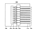
109 基板
110 V溝
120 光ファイバ
126 押圧部材
130 ファイバストッパ
132 張出部
134 取扱部
140 レンズアレイ
142 レンズ部
150 光源アレイ
152 LD
Claims (8)
- 表面を有し,前記表面側に溝群が整列して設けられた支持基板と;
前記表面上に配置された複数の光素子からなる光素子群と;
前記溝群の各溝に配置された光ファイバからなる光ファイバ群と;
複数の第1張出部と前記複数の第1張出部を接続する第1取扱部とを有し,前記複数の第1張出部が前記溝群の各溝にそれぞれ配置され,前記光ファイバの先端が当接されて前記光ファイバの光軸方向の位置決めを行う位置決め部材と;
前記光素子群の各光素子と前記光ファイバ群の各光ファイバとをそれぞれ光結合する複数のレンズ部と複数の第2張出部と前記複数の第2張出部を接続する第2取扱部とを有し,前記複数の第2張出部が前記溝群の各溝にそれぞれ配置され,前記光素子群と前記位置決め部材との間に配置されたレンズ素子と;
を備えることを特徴とする光モジュール。 - 光結合された前記光ファイバの当接する面と前記光素子とは光学的に共役の位置に配置されていることを特徴とする請求項1に記載の光モジュール。
- 前記光ファイバの当接する面の位置と前記光素子の位置とは,前記位置決め部材の屈折率を考慮して決められていることを特徴とする請求項2に記載の光モジュール。
- 前記光素子は発光素子であることを特徴とする請求項1〜3のいずれか1項に記載の光モジュール。
- 前記光素子は受光素子であることを特徴とする請求項1〜3のいずれか1項に記載の光モジュール。
- 前記光ファイバ群を前記溝群に押圧する押圧部材をさらに備え,前記支持基板上面から前記位置決め部材上端までの高さは,前記支持基板上面から前記押圧部材上端までの高さより高いことを特徴とする請求項1〜5のいずれか1項に記載の光モジュール。
- 表面を有し,第1の溝群と,前記第1の溝群と所定距離離れて対向するように設けられた第2の溝群とが前記表面側に整列して設けられた支持基板と;
前記支持基板の前記表面側の前記第1の溝群と前記第2の溝群との間に配置される光機能素子と;
前記第1の溝群の各溝に配置された光ファイバからなる第1の光ファイバ群と;
前記第2の溝群の各溝に配置された光ファイバからなる第2の光ファイバ群と;
複数の第1張出部と前記複数の第1張出部を接続する第1取扱部とを有し,前記複数の第1張出部が前記第1の溝群の各溝にそれぞれ配置され,前記第1の光ファイバ群の光ファイバの先端が当接されて前記光ファイバの光軸方向の位置決めを行う第1の位置決め部材と;
複数の第2張出部と前記複数の第2張出部を接続する第2取扱部とを有し,前記複数の第2張出部が前記第2の溝群の各溝にそれぞれ配置され,前記第2の光ファイバ群の光ファイバの先端が当接されて前記光ファイバの光軸方向の位置決めを行う第2の位置決め部材と;
前記光機能素子と前記第1の光ファイバ群の各光ファイバとをそれぞれ光結合する複数の第1レンズ部と複数の第3張出部と前記複数の第3張出部を接続する第3取扱部とを有し,前記複数の第3張出部が前記第1の溝群の各溝にそれぞれ配置され,前記光機能素子と前記第1の位置決め部材との間に配置された第1のレンズ素子と;
前記光機能素子と前記第2の光ファイバ群の各光ファイバとをそれぞれ光結合する複数の第2レンズ部と複数の第4張出部と前記複数の第4張出部を接続する第4取扱部とを有し,前記複数の第4張出部が前記第2の溝群の各溝にそれぞれ配置され,前記光機能素子と前記第2の位置決め部材との間に配置された第2のレンズ素子と;
を備えることを特徴とする光モジュール。 - 前記光ファイバ群を配置されている前記溝群に押圧する押圧部材をさらに備え,前記支持基板上面から前記位置決め部材上端までの高さは,前記支持基板上面から前記押圧部材上端までの高さより高いことを特徴とする請求項7に記載の光モジュール。
Priority Applications (1)
| Application Number | Priority Date | Filing Date | Title |
|---|---|---|---|
| JP2003420582A JP4089611B2 (ja) | 2003-12-18 | 2003-12-18 | 光モジュール |
Applications Claiming Priority (1)
| Application Number | Priority Date | Filing Date | Title |
|---|---|---|---|
| JP2003420582A JP4089611B2 (ja) | 2003-12-18 | 2003-12-18 | 光モジュール |
Publications (2)
| Publication Number | Publication Date |
|---|---|
| JP2005181584A JP2005181584A (ja) | 2005-07-07 |
| JP4089611B2 true JP4089611B2 (ja) | 2008-05-28 |
Family
ID=34782065
Family Applications (1)
| Application Number | Title | Priority Date | Filing Date |
|---|---|---|---|
| JP2003420582A Expired - Fee Related JP4089611B2 (ja) | 2003-12-18 | 2003-12-18 | 光モジュール |
Country Status (1)
| Country | Link |
|---|---|
| JP (1) | JP4089611B2 (ja) |
-
2003
- 2003-12-18 JP JP2003420582A patent/JP4089611B2/ja not_active Expired - Fee Related
Also Published As
| Publication number | Publication date |
|---|---|
| JP2005181584A (ja) | 2005-07-07 |
Similar Documents
| Publication | Publication Date | Title |
|---|---|---|
| JP4559327B2 (ja) | レンズを用いた光モジュールのアラインメント方法およびその方法で作成した光モジュール | |
| US7817883B2 (en) | Optical assembly and method of making same | |
| US8180189B2 (en) | Optical module and optical waveguide | |
| US6766076B2 (en) | Optical module and method for assembling the same | |
| US6985647B2 (en) | Optical module | |
| US8100589B2 (en) | Optical module and optical waveguide | |
| CN100451709C (zh) | 高耦合效率光电模块 | |
| JP3974480B2 (ja) | 光学部材の実装方法および光モジュール | |
| JP4008649B2 (ja) | 光学装置 | |
| JP2001305376A (ja) | コリメータアレイ装置の設計方法及びこの方法によって作製されたコリメータアレイ装置 | |
| US6870990B2 (en) | Optical device, optical device mounting method, and optical module | |
| JP3914124B2 (ja) | 光モジュール | |
| JP2002350673A (ja) | 光モジュールおよびその組立て方法 | |
| EP1335226B1 (en) | Optical lens or diffractive optical element and its manufacturing method | |
| JP4089611B2 (ja) | 光モジュール | |
| US7466502B2 (en) | Optical wavelength division coupler and associated methods | |
| US6739762B2 (en) | Optical device package | |
| US20250327981A1 (en) | Fiber array unit and photonics device | |
| JP4134942B2 (ja) | 光モジュール | |
| JP4200676B2 (ja) | 光学素子の製造方法 | |
| JPS6187113A (ja) | 導波形光モジユ−ルおよびその製造方法 | |
| JP2025101780A (ja) | 光導波路部品 | |
| JP2007086819A (ja) | 光モジュール | |
| KR0155507B1 (ko) | 광통신용 집적광학형 발광모듈 제작법 | |
| JP2000047070A (ja) | 光モジュール |
Legal Events
| Date | Code | Title | Description |
|---|---|---|---|
| A621 | Written request for application examination |
Free format text: JAPANESE INTERMEDIATE CODE: A621 Effective date: 20060221 |
|
| A131 | Notification of reasons for refusal |
Free format text: JAPANESE INTERMEDIATE CODE: A131 Effective date: 20070612 |
|
| A521 | Request for written amendment filed |
Free format text: JAPANESE INTERMEDIATE CODE: A523 Effective date: 20070809 |
|
| A131 | Notification of reasons for refusal |
Free format text: JAPANESE INTERMEDIATE CODE: A131 Effective date: 20070911 |
|
| A521 | Request for written amendment filed |
Free format text: JAPANESE INTERMEDIATE CODE: A523 Effective date: 20071019 |
|
| A131 | Notification of reasons for refusal |
Free format text: JAPANESE INTERMEDIATE CODE: A131 Effective date: 20071127 |
|
| A521 | Request for written amendment filed |
Free format text: JAPANESE INTERMEDIATE CODE: A523 Effective date: 20071205 |
|
| TRDD | Decision of grant or rejection written | ||
| A01 | Written decision to grant a patent or to grant a registration (utility model) |
Free format text: JAPANESE INTERMEDIATE CODE: A01 Effective date: 20080205 |
|
| A61 | First payment of annual fees (during grant procedure) |
Free format text: JAPANESE INTERMEDIATE CODE: A61 Effective date: 20080218 |
|
| R150 | Certificate of patent or registration of utility model |
Free format text: JAPANESE INTERMEDIATE CODE: R150 |
|
| FPAY | Renewal fee payment (event date is renewal date of database) |
Free format text: PAYMENT UNTIL: 20110307 Year of fee payment: 3 |
|
| FPAY | Renewal fee payment (event date is renewal date of database) |
Free format text: PAYMENT UNTIL: 20110307 Year of fee payment: 3 |
|
| S111 | Request for change of ownership or part of ownership |
Free format text: JAPANESE INTERMEDIATE CODE: R313111 |
|
| S531 | Written request for registration of change of domicile |
Free format text: JAPANESE INTERMEDIATE CODE: R313531 |
|
| FPAY | Renewal fee payment (event date is renewal date of database) |
Free format text: PAYMENT UNTIL: 20110307 Year of fee payment: 3 |
|
| R350 | Written notification of registration of transfer |
Free format text: JAPANESE INTERMEDIATE CODE: R350 |
|
| FPAY | Renewal fee payment (event date is renewal date of database) |
Free format text: PAYMENT UNTIL: 20110307 Year of fee payment: 3 |
|
| FPAY | Renewal fee payment (event date is renewal date of database) |
Free format text: PAYMENT UNTIL: 20120307 Year of fee payment: 4 |
|
| FPAY | Renewal fee payment (event date is renewal date of database) |
Free format text: PAYMENT UNTIL: 20120307 Year of fee payment: 4 |
|
| FPAY | Renewal fee payment (event date is renewal date of database) |
Free format text: PAYMENT UNTIL: 20130307 Year of fee payment: 5 |
|
| FPAY | Renewal fee payment (event date is renewal date of database) |
Free format text: PAYMENT UNTIL: 20140307 Year of fee payment: 6 |
|
| S531 | Written request for registration of change of domicile |
Free format text: JAPANESE INTERMEDIATE CODE: R313531 |
|
| S533 | Written request for registration of change of name |
Free format text: JAPANESE INTERMEDIATE CODE: R313533 |
|
| R350 | Written notification of registration of transfer |
Free format text: JAPANESE INTERMEDIATE CODE: R350 |
|
| LAPS | Cancellation because of no payment of annual fees |