JP4149404B2 - エバリュエーションチップ - Google Patents
エバリュエーションチップ Download PDFInfo
- Publication number
- JP4149404B2 JP4149404B2 JP2004093053A JP2004093053A JP4149404B2 JP 4149404 B2 JP4149404 B2 JP 4149404B2 JP 2004093053 A JP2004093053 A JP 2004093053A JP 2004093053 A JP2004093053 A JP 2004093053A JP 4149404 B2 JP4149404 B2 JP 4149404B2
- Authority
- JP
- Japan
- Prior art keywords
- interrupt
- priority
- signals
- signal
- control
- Prior art date
- Legal status (The legal status is an assumption and is not a legal conclusion. Google has not performed a legal analysis and makes no representation as to the accuracy of the status listed.)
- Expired - Fee Related
Links
Images


Classifications
-
- G—PHYSICS
- G06—COMPUTING OR CALCULATING; COUNTING
- G06F—ELECTRIC DIGITAL DATA PROCESSING
- G06F13/00—Interconnection of, or transfer of information or other signals between, memories, input/output devices or central processing units
- G06F13/14—Handling requests for interconnection or transfer
- G06F13/20—Handling requests for interconnection or transfer for access to input/output bus
- G06F13/24—Handling requests for interconnection or transfer for access to input/output bus using interrupt
- G06F13/26—Handling requests for interconnection or transfer for access to input/output bus using interrupt with priority control
Landscapes
- Engineering & Computer Science (AREA)
- Theoretical Computer Science (AREA)
- Physics & Mathematics (AREA)
- General Engineering & Computer Science (AREA)
- General Physics & Mathematics (AREA)
- Microcomputers (AREA)
- Test And Diagnosis Of Digital Computers (AREA)
Description
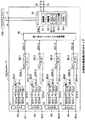
図1は、本発明の実施例1を示すEVAチップの概略の構成図である。
EVAチップ10を用いてプログラムメモリ100内のプログラムの評価を行う場合、マイコンコア50内のレジスタ部53からライトアドレスを出力し、このライトアドレスを出力端子17を介してプログラムメモリ100へ与え、そのライトアドレスに対応する命令を読み出す。読み出された命令は、入力端子16を介してマイコンコア50内の制御部51へ送られる。制御部51では、プログラムメモリ100からの命令を命令レジスタに一時記憶し、この記憶した命令を命令デコーダでデコードしてマイコンコア50内を制御する各種の制御信号を出力すると共に、ACCデータラッチ信号、RAMデータラッチ信号、及びRAMアドレスラッチ信号等を出力して複数の出力端子19から外部へ送出する。マイコンコア50内では、演算部52内のALU52−1及びACC52−2等を用いて演算を行い、プログラムメモリ100からの命令を実行してこの命令実行結果をRAM54等に格納し、複数の出力端子18から外部へ送出する。
入力端子11−1〜11−4に与える制御信号S11の電位;0,0,0,1
入力端子12−1〜12−4に与える制御信号S12の電位;1,0,0,0
入力端子13−1〜13−4に与える制御信号S13の電位;0,0,1,0
入力端子14−1〜14−4に与える制御信号S14の電位;0,1,0,0
本実施例1では、外部から入力端子11−1〜11−4,12−1〜12−4,13−1〜13−4,14−1〜14−4に与える制御信号S11〜S14の電位により、各割り込みモジュール30−1〜30−4の割り込み優先順位を任意に変更可能な構成にしたので、割り込みモジュール30−1〜30−4の優先順位が異なるマイコンコア50に対して、1種類のEVAチップ10で対応可能となり、使い勝手が良く、コストを削減できる。
図2は、本発明の実施例2を示すEVAチップの概略の構成図であり、実施例1を示す図1中の要素と共通の要素には共通の符号が付されている。
EVAチップ10Aを用いてプログラムメモリ100内のプラグラムの評価を行う場合は、実施例1と同様に動作する。
優先順位制御レジスタ71の4ビット出力端子の電位;01H(=0,0,0,1)
優先順位制御レジスタ72の4ビット出力端子の電位;08H(=1,0,0,0)
優先順位制御レジスタ73の4ビット出力端子の電位;02H(=0,0,1,0)
優先順位制御レジスタ74の4ビット出力端子の電位;04H(=0,1,0,0)
本実施例2では、次の(1)、(2)のような効果がある。
図3は、本発明の実施例3を示すEVAチップの概略の構成図であり、実施例1、2を示す図1、図2中の要素と共通の要素には共通の符号が付されている。
EVAチップ10Bを用いてプログラムメモリ100内のプラグラムの評価を行う場合は、実施例1、2と同様に動作する。
シリアル12ビットデータS81;
0,0,0,1/1,0,0,0/0,0,1,0/0,1,0,0
本実施例3では、次の(1)、(2)のような効果がある。
11−1〜11−4,12−1〜12−4,13−1〜13−4、14−1〜14−4 制御信号入力端子
15−1〜15−4 割り込み要求信号入力端子
20−1〜20−4 割り込み優先順位決定回路
30−1〜30−4 割り込みモジュール
40 割り込みベクタアドレス生成回路
50 マイコンコア
71〜74 優先順位制御レジスタ
90 割り込み優先順位制御シフトレジスタ
100 プログラムメモリ
Claims (4)
- 割り込み変更信号を出力する複数の割り込み優先順位決定回路と、割り込み信号を出力する複数の割り込み信号生成回路と、割り込みベクタアドレス生成回路と、命令実行手段とを備え、
外部から与えられる複数の割り込み要求信号に基づき、対応する割り込み処理を順に実行するエバリュエーションチップにおいて、
前記割り込み優先順位決定回路は、対応する前記割り込み信号生成回路以外が生成した複数の前記割り込み信号と、外部から与えられる割り込み優先順位変更制御用の複数の制御信号との論理を求めて、前記割り込み変更信号を出力し、
前記割り込み信号生成回路は、対応する前記割り込み優先順位決定回路が出力する前記割り込み変更信号と、対応する前記割り込み要求信号との論理を求めて、前記複数の割り込み要求信号の全てが発生しているときに、前記複数の制御信号で設定される優先順位に従って、前記割り込み信号を順に生成し、
前記割り込みベクタアドレス生成回路は、複数の前記割り込み信号をエンコードして割り込みベクタアドレスを生成し、
前記命令実行手段は、前記割り込みベクタアドレスに基づき、外部から優先順に取り込んだ割り込み命令をデコードしてこのデコード結果を順に実行すること
を特徴とするエバリュエーションチップ。 - 前記複数の制御信号は、外部の制御信号入力端子から入力される構成にしたことを特徴とする請求項1記載のエバリュエーションチップ。
- 前記複数の制御信号は、外部から与えられるデータに基づき、内部に設けた複数の優先順位制御レジスタにより生成する構成にしたことを特徴とする請求項1記載のエバリュエーションチップ。
- 前記複数の制御信号は、外部から与えられるシリアルデータに基づき、内部に設けた割り込み優先順位制御シフトレジスタにより、パワーオン時に生成する構成にしたことを特徴とする請求項1記載のエバリュエーションチップ。
Priority Applications (3)
| Application Number | Priority Date | Filing Date | Title |
|---|---|---|---|
| JP2004093053A JP4149404B2 (ja) | 2004-03-26 | 2004-03-26 | エバリュエーションチップ |
| US10/989,025 US7159057B2 (en) | 2004-03-26 | 2004-11-16 | Evaluation chip |
| CNB2004100114418A CN100511170C (zh) | 2004-03-26 | 2004-12-20 | 评估芯片 |
Applications Claiming Priority (1)
| Application Number | Priority Date | Filing Date | Title |
|---|---|---|---|
| JP2004093053A JP4149404B2 (ja) | 2004-03-26 | 2004-03-26 | エバリュエーションチップ |
Publications (2)
| Publication Number | Publication Date |
|---|---|
| JP2005284354A JP2005284354A (ja) | 2005-10-13 |
| JP4149404B2 true JP4149404B2 (ja) | 2008-09-10 |
Family
ID=34991491
Family Applications (1)
| Application Number | Title | Priority Date | Filing Date |
|---|---|---|---|
| JP2004093053A Expired - Fee Related JP4149404B2 (ja) | 2004-03-26 | 2004-03-26 | エバリュエーションチップ |
Country Status (3)
| Country | Link |
|---|---|
| US (1) | US7159057B2 (ja) |
| JP (1) | JP4149404B2 (ja) |
| CN (1) | CN100511170C (ja) |
Families Citing this family (4)
| Publication number | Priority date | Publication date | Assignee | Title |
|---|---|---|---|---|
| US7839164B1 (en) * | 2009-05-14 | 2010-11-23 | Lsi Corporation | Low depth programmable priority encoders |
| US8352804B2 (en) * | 2010-05-20 | 2013-01-08 | Infineon Technologies Ag | Systems and methods for secure interrupt handling |
| US20140089646A1 (en) * | 2012-09-27 | 2014-03-27 | Texas Instruments Incorporated | Processor with interruptable instruction execution |
| EP3940544B1 (de) * | 2020-07-14 | 2026-01-28 | VEGA Grieshaber KG | Verfahren zur datenübertragung und schaltungsanordnung dafür |
Family Cites Families (6)
| Publication number | Priority date | Publication date | Assignee | Title |
|---|---|---|---|---|
| JPH05151014A (ja) | 1991-11-29 | 1993-06-18 | Oki Electric Ind Co Ltd | エバリユエーシヨンチツプ |
| US5594905A (en) * | 1995-04-12 | 1997-01-14 | Microsoft Corporation | Exception handler and method for handling interrupts |
| US6539448B1 (en) * | 2000-05-26 | 2003-03-25 | Texas Instruments Incorporated | Priority first come first serve interrupt controller |
| GB2396445B (en) * | 2002-12-19 | 2005-12-21 | Advanced Risc Mach Ltd | An interrupt controller and interrupt controlling method for prioritizing interrupt requests generated by a plurality of interrupt sources |
| GB2403822B (en) * | 2003-07-07 | 2006-05-10 | Advanced Risc Mach Ltd | Data processing apparatus and method for handling interrupts |
| US7139857B2 (en) * | 2003-11-12 | 2006-11-21 | Standard Microsystems Corporation | Method and apparatus for handling interrupts |
-
2004
- 2004-03-26 JP JP2004093053A patent/JP4149404B2/ja not_active Expired - Fee Related
- 2004-11-16 US US10/989,025 patent/US7159057B2/en not_active Expired - Fee Related
- 2004-12-20 CN CNB2004100114418A patent/CN100511170C/zh not_active Expired - Fee Related
Also Published As
| Publication number | Publication date |
|---|---|
| CN100511170C (zh) | 2009-07-08 |
| US7159057B2 (en) | 2007-01-02 |
| US20050216636A1 (en) | 2005-09-29 |
| JP2005284354A (ja) | 2005-10-13 |
| CN1673973A (zh) | 2005-09-28 |
Similar Documents
| Publication | Publication Date | Title |
|---|---|---|
| TWI476597B (zh) | 資料處理裝置及半導體積體電路裝置 | |
| US11086816B2 (en) | Processors, methods, and systems for debugging a configurable spatial accelerator | |
| JPS62249226A (ja) | プログラム可能論理装置およびその方法 | |
| KR20000076310A (ko) | 리스크 구조를 갖는 8 비트 마이크로콘트롤러 | |
| ITMI981564A1 (it) | Memoria non volatile in grado di eseguire un programma autonomamente | |
| JP4149404B2 (ja) | エバリュエーションチップ | |
| JP2004086837A (ja) | データ処理装置 | |
| JP2993975B2 (ja) | 中央演算処理装置 | |
| US20210117189A1 (en) | Reduced instruction set processor based on memristor | |
| JP4391053B2 (ja) | 複数の独立の専用プロセッサを有するデジタル信号プロセッサ | |
| US6304958B1 (en) | Microcomputer having data execution units mounted thereon | |
| JP2006018411A (ja) | プロセッサ | |
| JP4545777B2 (ja) | データ処理装置 | |
| JPH0475137A (ja) | データ処理装置 | |
| JPH03129425A (ja) | ビットフィールド論理演算処理装置およびそれを具備するモノリシックマイクロプロセッサ | |
| JP5025521B2 (ja) | 半導体装置 | |
| JP2001344116A (ja) | 演算処理装置 | |
| KR100631495B1 (ko) | 마이크로 프로세서 | |
| KR100318315B1 (ko) | 원칩마이크로컴퓨터 | |
| Pandya et al. | Implement embedded controller using FPGA chip | |
| KR100737802B1 (ko) | 모듈형 디지털 신호 프로세서 블록 및 이를 이용한시스템-온-칩 | |
| Trost et al. | Design of custom processors for the fpga devices | |
| Pohronská et al. | Fault-tolerant embedded systems with multiple FPGA implemented watchdogs | |
| JP4702004B2 (ja) | マイクロコンピュータ | |
| JP4498338B2 (ja) | データ処理装置 |
Legal Events
| Date | Code | Title | Description |
|---|---|---|---|
| A621 | Written request for application examination |
Free format text: JAPANESE INTERMEDIATE CODE: A621 Effective date: 20060825 |
|
| A131 | Notification of reasons for refusal |
Free format text: JAPANESE INTERMEDIATE CODE: A131 Effective date: 20080401 |
|
| A521 | Request for written amendment filed |
Free format text: JAPANESE INTERMEDIATE CODE: A523 Effective date: 20080529 |
|
| TRDD | Decision of grant or rejection written | ||
| A01 | Written decision to grant a patent or to grant a registration (utility model) |
Free format text: JAPANESE INTERMEDIATE CODE: A01 Effective date: 20080624 |
|
| A01 | Written decision to grant a patent or to grant a registration (utility model) |
Free format text: JAPANESE INTERMEDIATE CODE: A01 |
|
| A61 | First payment of annual fees (during grant procedure) |
Free format text: JAPANESE INTERMEDIATE CODE: A61 Effective date: 20080625 |
|
| FPAY | Renewal fee payment (event date is renewal date of database) |
Free format text: PAYMENT UNTIL: 20110704 Year of fee payment: 3 |
|
| R150 | Certificate of patent or registration of utility model |
Ref document number: 4149404 Country of ref document: JP Free format text: JAPANESE INTERMEDIATE CODE: R150 |
|
| FPAY | Renewal fee payment (event date is renewal date of database) |
Free format text: PAYMENT UNTIL: 20110704 Year of fee payment: 3 |
|
| S111 | Request for change of ownership or part of ownership |
Free format text: JAPANESE INTERMEDIATE CODE: R313115 |
|
| S531 | Written request for registration of change of domicile |
Free format text: JAPANESE INTERMEDIATE CODE: R313531 |
|
| FPAY | Renewal fee payment (event date is renewal date of database) |
Free format text: PAYMENT UNTIL: 20110704 Year of fee payment: 3 |
|
| R350 | Written notification of registration of transfer |
Free format text: JAPANESE INTERMEDIATE CODE: R350 |
|
| FPAY | Renewal fee payment (event date is renewal date of database) |
Free format text: PAYMENT UNTIL: 20120704 Year of fee payment: 4 |
|
| FPAY | Renewal fee payment (event date is renewal date of database) |
Free format text: PAYMENT UNTIL: 20120704 Year of fee payment: 4 |
|
| FPAY | Renewal fee payment (event date is renewal date of database) |
Free format text: PAYMENT UNTIL: 20130704 Year of fee payment: 5 |
|
| S531 | Written request for registration of change of domicile |
Free format text: JAPANESE INTERMEDIATE CODE: R313531 |
|
| S533 | Written request for registration of change of name |
Free format text: JAPANESE INTERMEDIATE CODE: R313533 |
|
| S111 | Request for change of ownership or part of ownership |
Free format text: JAPANESE INTERMEDIATE CODE: R313111 |
|
| R350 | Written notification of registration of transfer |
Free format text: JAPANESE INTERMEDIATE CODE: R350 |
|
| R360 | Written notification for declining of transfer of rights |
Free format text: JAPANESE INTERMEDIATE CODE: R360 |
|
| R370 | Written measure of declining of transfer procedure |
Free format text: JAPANESE INTERMEDIATE CODE: R370 |
|
| S111 | Request for change of ownership or part of ownership |
Free format text: JAPANESE INTERMEDIATE CODE: R313115 |
|
| R350 | Written notification of registration of transfer |
Free format text: JAPANESE INTERMEDIATE CODE: R350 |
|
| R250 | Receipt of annual fees |
Free format text: JAPANESE INTERMEDIATE CODE: R250 |
|
| R250 | Receipt of annual fees |
Free format text: JAPANESE INTERMEDIATE CODE: R250 |
|
| LAPS | Cancellation because of no payment of annual fees |