JP4170246B2 - Vertical bipolar transistor - Google Patents
Vertical bipolar transistor Download PDFInfo
- Publication number
- JP4170246B2 JP4170246B2 JP2004090598A JP2004090598A JP4170246B2 JP 4170246 B2 JP4170246 B2 JP 4170246B2 JP 2004090598 A JP2004090598 A JP 2004090598A JP 2004090598 A JP2004090598 A JP 2004090598A JP 4170246 B2 JP4170246 B2 JP 4170246B2
- Authority
- JP
- Japan
- Prior art keywords
- region
- intrinsic base
- base region
- sti
- substrate
- Prior art date
- Legal status (The legal status is an assumption and is not a legal conclusion. Google has not performed a legal analysis and makes no representation as to the accuracy of the status listed.)
- Expired - Fee Related
Links
- 238000002955 isolation Methods 0.000 claims abstract description 173
- 239000000758 substrate Substances 0.000 claims abstract description 70
- XUIMIQQOPSSXEZ-UHFFFAOYSA-N Silicon Chemical compound [Si] XUIMIQQOPSSXEZ-UHFFFAOYSA-N 0.000 claims abstract description 32
- 229910052710 silicon Inorganic materials 0.000 claims abstract description 32
- 239000010703 silicon Substances 0.000 claims abstract description 32
- 239000003989 dielectric material Substances 0.000 claims abstract description 26
- 239000004065 semiconductor Substances 0.000 claims abstract description 17
- 229910021420 polycrystalline silicon Inorganic materials 0.000 claims description 48
- 229920005591 polysilicon Polymers 0.000 claims description 41
- 229910052581 Si3N4 Inorganic materials 0.000 claims description 38
- HQVNEWCFYHHQES-UHFFFAOYSA-N silicon nitride Chemical compound N12[Si]34N5[Si]62N3[Si]51N64 HQVNEWCFYHHQES-UHFFFAOYSA-N 0.000 claims description 36
- 239000000463 material Substances 0.000 claims description 20
- 125000006850 spacer group Chemical group 0.000 claims description 17
- 229910000577 Silicon-germanium Inorganic materials 0.000 claims description 13
- LEVVHYCKPQWKOP-UHFFFAOYSA-N [Si].[Ge] Chemical compound [Si].[Ge] LEVVHYCKPQWKOP-UHFFFAOYSA-N 0.000 claims description 8
- 230000003071 parasitic effect Effects 0.000 abstract description 28
- 239000010410 layer Substances 0.000 description 128
- 238000000034 method Methods 0.000 description 64
- 229910052814 silicon oxide Inorganic materials 0.000 description 43
- 238000004519 manufacturing process Methods 0.000 description 41
- VYPSYNLAJGMNEJ-UHFFFAOYSA-N Silicium dioxide Chemical compound O=[Si]=O VYPSYNLAJGMNEJ-UHFFFAOYSA-N 0.000 description 39
- 238000005530 etching Methods 0.000 description 23
- NJPPVKZQTLUDBO-UHFFFAOYSA-N novaluron Chemical compound C1=C(Cl)C(OC(F)(F)C(OC(F)(F)F)F)=CC=C1NC(=O)NC(=O)C1=C(F)C=CC=C1F NJPPVKZQTLUDBO-UHFFFAOYSA-N 0.000 description 20
- 230000008569 process Effects 0.000 description 18
- 238000012545 processing Methods 0.000 description 14
- 229920002120 photoresistant polymer Polymers 0.000 description 13
- 230000015572 biosynthetic process Effects 0.000 description 11
- 238000000151 deposition Methods 0.000 description 9
- 230000004048 modification Effects 0.000 description 7
- 238000012986 modification Methods 0.000 description 7
- 230000003647 oxidation Effects 0.000 description 6
- 238000007254 oxidation reaction Methods 0.000 description 6
- 238000000926 separation method Methods 0.000 description 5
- 230000002093 peripheral effect Effects 0.000 description 4
- 239000011241 protective layer Substances 0.000 description 4
- 239000002019 doping agent Substances 0.000 description 3
- 229910021332 silicide Inorganic materials 0.000 description 3
- FVBUAEGBCNSCDD-UHFFFAOYSA-N silicide(4-) Chemical compound [Si-4] FVBUAEGBCNSCDD-UHFFFAOYSA-N 0.000 description 3
- 239000000126 substance Substances 0.000 description 3
- NBIIXXVUZAFLBC-UHFFFAOYSA-N Phosphoric acid Chemical compound OP(O)(O)=O NBIIXXVUZAFLBC-UHFFFAOYSA-N 0.000 description 2
- 230000008859 change Effects 0.000 description 2
- 239000002131 composite material Substances 0.000 description 2
- 239000013078 crystal Substances 0.000 description 2
- 238000013461 design Methods 0.000 description 2
- 238000009792 diffusion process Methods 0.000 description 2
- 230000000694 effects Effects 0.000 description 2
- 238000000407 epitaxy Methods 0.000 description 2
- 239000002184 metal Substances 0.000 description 2
- 238000005457 optimization Methods 0.000 description 2
- 230000010355 oscillation Effects 0.000 description 2
- 238000000059 patterning Methods 0.000 description 2
- 238000001039 wet etching Methods 0.000 description 2
- VHUUQVKOLVNVRT-UHFFFAOYSA-N Ammonium hydroxide Chemical compound [NH4+].[OH-] VHUUQVKOLVNVRT-UHFFFAOYSA-N 0.000 description 1
- KRHYYFGTRYWZRS-UHFFFAOYSA-M Fluoride anion Chemical compound [F-] KRHYYFGTRYWZRS-UHFFFAOYSA-M 0.000 description 1
- CBENFWSGALASAD-UHFFFAOYSA-N Ozone Chemical compound [O-][O+]=O CBENFWSGALASAD-UHFFFAOYSA-N 0.000 description 1
- BOTDANWDWHJENH-UHFFFAOYSA-N Tetraethyl orthosilicate Chemical compound CCO[Si](OCC)(OCC)OCC BOTDANWDWHJENH-UHFFFAOYSA-N 0.000 description 1
- 239000002253 acid Substances 0.000 description 1
- 230000002411 adverse Effects 0.000 description 1
- 229910000147 aluminium phosphate Inorganic materials 0.000 description 1
- 239000000908 ammonium hydroxide Substances 0.000 description 1
- 230000004888 barrier function Effects 0.000 description 1
- 238000007796 conventional method Methods 0.000 description 1
- 230000008021 deposition Effects 0.000 description 1
- 229910052732 germanium Inorganic materials 0.000 description 1
- GNPVGFCGXDBREM-UHFFFAOYSA-N germanium atom Chemical compound [Ge] GNPVGFCGXDBREM-UHFFFAOYSA-N 0.000 description 1
- 238000011065 in-situ storage Methods 0.000 description 1
- 238000005468 ion implantation Methods 0.000 description 1
- 238000001459 lithography Methods 0.000 description 1
- 238000004518 low pressure chemical vapour deposition Methods 0.000 description 1
- 229910021421 monocrystalline silicon Inorganic materials 0.000 description 1
- 230000001590 oxidative effect Effects 0.000 description 1
- 238000000623 plasma-assisted chemical vapour deposition Methods 0.000 description 1
- 238000001289 rapid thermal chemical vapour deposition Methods 0.000 description 1
- 230000009467 reduction Effects 0.000 description 1
Images


Classifications
-
- H—ELECTRICITY
- H10—SEMICONDUCTOR DEVICES; ELECTRIC SOLID-STATE DEVICES NOT OTHERWISE PROVIDED FOR
- H10D—INORGANIC ELECTRIC SEMICONDUCTOR DEVICES
- H10D48/00—Individual devices not covered by groups H10D1/00 - H10D44/00
- H10D48/30—Devices controlled by electric currents or voltages
- H10D48/32—Devices controlled by only the electric current supplied, or only the electric potential applied, to an electrode which does not carry the current to be rectified, amplified or switched
- H10D48/34—Bipolar devices
-
- H—ELECTRICITY
- H10—SEMICONDUCTOR DEVICES; ELECTRIC SOLID-STATE DEVICES NOT OTHERWISE PROVIDED FOR
- H10D—INORGANIC ELECTRIC SEMICONDUCTOR DEVICES
- H10D10/00—Bipolar junction transistors [BJT]
- H10D10/01—Manufacture or treatment
- H10D10/051—Manufacture or treatment of vertical BJTs
- H10D10/054—Forming extrinsic base regions on silicon substrate after insulating device isolation in vertical BJTs having single crystalline emitter, collector or base regions
-
- H—ELECTRICITY
- H10—SEMICONDUCTOR DEVICES; ELECTRIC SOLID-STATE DEVICES NOT OTHERWISE PROVIDED FOR
- H10D—INORGANIC ELECTRIC SEMICONDUCTOR DEVICES
- H10D10/00—Bipolar junction transistors [BJT]
- H10D10/01—Manufacture or treatment
- H10D10/021—Manufacture or treatment of heterojunction BJTs [HBT]
-
- H—ELECTRICITY
- H10—SEMICONDUCTOR DEVICES; ELECTRIC SOLID-STATE DEVICES NOT OTHERWISE PROVIDED FOR
- H10D—INORGANIC ELECTRIC SEMICONDUCTOR DEVICES
- H10D10/00—Bipolar junction transistors [BJT]
- H10D10/40—Vertical BJTs
-
- H—ELECTRICITY
- H10—SEMICONDUCTOR DEVICES; ELECTRIC SOLID-STATE DEVICES NOT OTHERWISE PROVIDED FOR
- H10D—INORGANIC ELECTRIC SEMICONDUCTOR DEVICES
- H10D10/00—Bipolar junction transistors [BJT]
- H10D10/80—Heterojunction BJTs
- H10D10/821—Vertical heterojunction BJTs
- H10D10/891—Vertical heterojunction BJTs comprising lattice-mismatched active layers, e.g. SiGe strained-layer transistors
-
- H—ELECTRICITY
- H10—SEMICONDUCTOR DEVICES; ELECTRIC SOLID-STATE DEVICES NOT OTHERWISE PROVIDED FOR
- H10D—INORGANIC ELECTRIC SEMICONDUCTOR DEVICES
- H10D62/00—Semiconductor bodies, or regions thereof, of devices having potential barriers
- H10D62/10—Shapes, relative sizes or dispositions of the regions of the semiconductor bodies; Shapes of the semiconductor bodies
- H10D62/113—Isolations within a component, i.e. internal isolations
- H10D62/115—Dielectric isolations, e.g. air gaps
Landscapes
- Bipolar Transistors (AREA)
Abstract
Description
本発明は、バイポーラ・トランジスタ構造、特に、寄生容量を低減した構造およびその製造方法に関する。 The present invention relates to a bipolar transistor structure, and more particularly to a structure with reduced parasitic capacitance and a manufacturing method thereof.
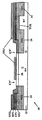
図1は、シリコン半導体基板上に形成された従来技術の縦型バイポーラ・トランジスタの断面図である。縦型バイポーラ・トランジスタは、従来のバイポーラ・デバイス設計に従って、ドープト・エミッタE,ドープト・コレクタC,カウンタドープト複合ベースを有している。コレクタCは、シリコン半導体基板の表面内の1対の浅いトレンチ分離(STI)(誘電体)領域の間に形成される。複合ベースは、シリコン(Si)またはシリコン・ゲルマニウム(Si−Ge)の真性ベース領域と、この真性ベース領域上の外部ベース領域とを有している。コレクタC上に重なり、エミッタ領域により取り囲まれたドープト・真性ベース領域は、コレクタ領域およびエミッタ領域と物理的および電気的に接触している。外部ベース領域は、真性ベース領域およびSTI領域の一部分外面上にある。エミッタ領域は、真性ベース領域上に形成され、誘電体領域によって外部ベース領域から分離されている。デバイスのベース/コレクタ間容量(Ccb)は、(1)(エミッタ開口によって画成される)アクティブ領域の内側のベースとコレクタとの間の成分、(2)アクティブ領域の外側であってSTIエッジの内側のベースとコレクタとの間との成分、(3)STI領域でのベースとコレクタとの間の成分との合計である。 FIG. 1 is a cross-sectional view of a prior art vertical bipolar transistor formed on a silicon semiconductor substrate. The vertical bipolar transistor has a doped emitter E, a doped collector C, and a counter-doped composite base according to a conventional bipolar device design. The collector C is formed between a pair of shallow trench isolation (STI) (dielectric) regions in the surface of the silicon semiconductor substrate. The composite base has an intrinsic base region of silicon (Si) or silicon germanium (Si-Ge) and an external base region on the intrinsic base region. The doped intrinsic base region that overlies the collector C and is surrounded by the emitter region is in physical and electrical contact with the collector region and the emitter region. The external base region is on a part of the outer surface of the intrinsic base region and the STI region. The emitter region is formed on the intrinsic base region and is separated from the external base region by a dielectric region. The base-collector capacitance (C cb ) of the device is (1) the component between the base and collector inside the active area (defined by the emitter aperture), (2) the STI outside the active area The sum of the components between the base and the collector inside the edge, and (3) the components between the base and the collector in the STI region.
カットオフ周波数(fT)および最大発振周波数(fmax)は、高速トランジスタの動作速度を最も代表的なパラメータである。したがって、高速トランジスタのための設計および最適化の試みは、ほとんど、これら2つのパラメータの最大化に向けられている。カットオフ周波数(fT)および最大発振周波数(fmax)に影響を与えるデバイス・パラメータの1つは、ベース/コレクタ間容量(Ccb)である。エミッタ抵抗,コレクタ抵抗、およびデバイス相互コンダクタンスに関係するRC遅延(充電時間)が増大する結果、Ccbが増大して、fTの値が減少する。Ccbに関係したRC遅延にfmaxがより敏感であるので、fmaxへのCcbの影響は、かなり大きい。特に、fTおよびfmaxすなわちデバイスの動作速度に大きなインパクトを与えるデバイス成分(抵抗および容量)は、Ccbである。したがって、寄生成分の低減によってデバイス速度を改善する最も有効な方法は、Ccbの外部(extrinsic)成分を最小化することである。 The cut-off frequency (f T ) and the maximum oscillation frequency (f max ) are the most representative parameters of the operation speed of the high-speed transistor. Therefore, most design and optimization efforts for high speed transistors are directed to maximizing these two parameters. One of the device parameters that affects the cut-off frequency (f T ) and the maximum oscillation frequency (f max ) is the base / collector capacitance (C cb ). Increasing RC delay (charge time) related to emitter resistance, collector resistance, and device transconductance results in an increase in C cb and a decrease in the value of f T. Since f max to the RC delay related to the C cb is more sensitive, the effect of C cb to f max is much greater. In particular, f T and f max, that is, a device component (resistance and capacitance) that has a large impact on the operation speed of the device is C cb . Thus, the most effective way to improve device speed by reducing parasitic components is to minimize the extrinsic component of C cb .
Ccbの外部成分すなわち寄生成分は、通常のバイポーラ・トランジスタの全Ccbの半分以上を含んでいる。この寄生容量は、アクティブ・トランジスタ領域の外側であって、浅いトレンチ分離(STI)領域上に延在する、コレクタ領域とベース(真性および外部)領域との間の重なりにより生じる。これらの領域の間の重なりは、寸法を最小にし、基板上のデバイス密度を増大させる要件によって課される重なり公差および位置決め公差の制限の故に、リソグラフィによって最小化できない。さらに、寄生容量は、ベース領域からコレクタ領域へのドーパントの拡散によって、さらに増大する。したがって、寄生成分を低減するデバイスの構造的最適化は、fTおよびfmax(すなわち、デバイスの動作速度)の改善に対するキーである。 External component, that parasitics C cb includes more than half of the total C cb conventional bipolar transistor. This parasitic capacitance is caused by the overlap between the collector and base (intrinsic and external) regions that extend outside the active transistor region and over the shallow trench isolation (STI) region. The overlap between these regions cannot be minimized by lithography due to the overlap and positioning tolerance limitations imposed by the requirements of minimizing dimensions and increasing device density on the substrate. Furthermore, the parasitic capacitance is further increased by dopant diffusion from the base region to the collector region. Therefore, structural optimization of the device to reduce parasitic components is key to improving f T and f max (ie, device operating speed).
特許文献1は、ベースにSiGeを用いることを教示し、およびコレクタ・エピタキシャル層とベース電極単結晶シリコン膜との間に形成される寄生容量は、これらの間の距離が約1000Åに設定されるので、低減されることを教示している。従来技術の方法で寄生容量を低減するためには、真性ベースを厚くしなければならず、したがってカットオフ周波数fTが低下する。選択的エピタキシャル成長によって形成される単結晶構造のシリコンが、ベース電極に用いられて、特にSiGeのベースを構成することによって、ベースとコレクタとの間の寄生容量を低減している。コレクタ領域を含むデバイス全体が、シリコン半導体基板の表面上に形成される。寄生容量を低減する方法は、選択的エピタキシを用いて、真性ベースを成長させることである。 Patent Document 1 teaches using SiGe for the base, and the parasitic capacitance formed between the collector epitaxial layer and the base electrode single crystal silicon film is set to a distance of about 1000 mm between them. So it is taught to be reduced. To reduce the parasitic capacitance in the prior art methods, it is necessary to increase the thickness of the intrinsic base, thus the cut-off frequency f T is lowered. Silicon having a single crystal structure formed by selective epitaxial growth is used for the base electrode, and in particular constitutes the base of SiGe, thereby reducing the parasitic capacitance between the base and the collector. The entire device including the collector region is formed on the surface of the silicon semiconductor substrate. A way to reduce parasitic capacitance is to grow the intrinsic base using selective epitaxy.
特許文献2は、自己整合縦型バイポーラ・トランジスタ構造と、正しい位置決めを与えることにより実現される「低減したベース/コレクタ間寄生容量」を有する構造を製造する方法とを記述している。特許文献2の手段は、ベース/コレクタ間寄生容量の問題を解決する本発明の現在の手段と類似している。しかし、本発明の技法は、特許文献2に記載されていない特徴(後述)を有している。
本発明の目的は、バイポーラ・トランジスタ構造、特に、寄生容量を低減したバイポーラ・トランジスタ構造およびその製造方法を提供することにある。 An object of the present invention is to provide a bipolar transistor structure, in particular, a bipolar transistor structure with reduced parasitic capacitance and a method for manufacturing the same.
本発明によれば、バイポーラ・トランジスタにおいてCcbの寄生成分を低減させる構造的変形が、他のパラメータへの悪影響を最小にして提供される。特に、コレクタとベースとの間の過剰な重なり領域を、外部ベース領域を形成する前に、部分的に除去して、誘電体で充てんする。誘電体は、コレクタと外部ベースとを分離し、ドーパント拡散に対するバリアとして働き、Ccbの寄生成分を低減する。典型的なシリコンをベースとしたバイポーラ・トランジスタにおけるCcbの寄生成分は、デバイスの外部ベース部分(extrinsic part)に形成されたベース・コレクタのPN接合の空乏領域の存在の結果である。本発明によれば、このようなトランジスタにおける寄生容量は、空乏領域内に低い誘電率の材料を用いることによって低減される。というのは、シリコンは高い誘電率を有するからである。 In accordance with the present invention, structural modifications that reduce the parasitic component of C cb in bipolar transistors are provided with minimal adverse effects on other parameters. In particular, the excess overlap region between the collector and the base is partially removed and filled with a dielectric before forming the outer base region. The dielectric separates the collector from the external base, acts as a barrier to dopant diffusion, and reduces the parasitic component of C cb . The parasitic component of C cb in a typical silicon-based bipolar transistor is the result of the presence of a depletion region in the base-collector PN junction formed in the extrinsic part of the device. According to the present invention, the parasitic capacitance in such a transistor is reduced by using a low dielectric constant material in the depletion region. This is because silicon has a high dielectric constant.
本発明によれば、シリコン空乏領域が、低誘電率の誘電体材料で、部分的にまたは全部が置き換えられる。実施例によれば、誘電体の1つの選択は、酸化シリコンであり、その誘電率は、シリコンの33%であり、容量をかなり低減する。 In accordance with the present invention, the silicon depletion region is partially or wholly replaced with a low dielectric constant dielectric material. According to an embodiment, one choice of dielectric is silicon oxide, whose dielectric constant is 33% of silicon, significantly reducing capacitance.
本発明によれば、縦型バイポーラ・トランジスタが、上面を有するシリコン半導体基板内に形成される。基板内には、誘電体材料よりなり内側端部と上面とを有するSTI領域が形成される。ドープト・コレクタ領域が、基板内であって、1対のSTI領域の間に形成される。カウンタドープト・真性ベース領域が、基板の上面であって、1対のSTI領域の間に形成される。真性ベース領域と1対のSTI領域との間にマージンがあり、真性ベース領域はエッジを有する。ドープト・エミッタ領域が、真性ベース領域上に、エッジから離れて形成される。誘電体材料よりなる浅い分離エクステンション領域が、STI領域と真性ベース領域との間のマージン内に形成され、真性ベース領域のエッジと並置される。外部ベース領域が、浅い分離エクステンション領域を覆い、真性ベース領域上に部分的に延びて物理的および電気的に接触する。これにより、浅い分離エクステンション領域は、バイポーラ・トランジスタのベース/コレクタ間寄生容量を低減する。好ましくは、浅い分離エクステンション領域は、エミッタの側壁スペーサをマスクにして形成されているか、あるいは浅い分離エクステンション領域は、エミッタの側壁スペーサをマスクに形成されていない。 In accordance with the present invention, a vertical bipolar transistor is formed in a silicon semiconductor substrate having an upper surface. An STI region made of a dielectric material and having an inner end and an upper surface is formed in the substrate. A doped collector region is formed in the substrate and between a pair of STI regions. A counter-doped intrinsic base region is formed between the pair of STI regions on the top surface of the substrate. There is a margin between the intrinsic base region and the pair of STI regions, and the intrinsic base region has an edge. A doped emitter region is formed on the intrinsic base region away from the edge. A shallow isolation extension region of dielectric material is formed in the margin between the STI region and the intrinsic base region and juxtaposed with the edge of the intrinsic base region. An external base region covers the shallow isolation extension region and extends partially over the intrinsic base region to make physical and electrical contact. Thereby, the shallow isolation extension region reduces the base-collector parasitic capacitance of the bipolar transistor. Preferably, the shallow isolation extension region is formed using the emitter sidewall spacer as a mask , or the shallow isolation extension region is not formed using the emitter sidewall spacer as a mask .
好ましくは、浅い分離エクステンション領域は、酸化されたドープト・シリコンと付着された酸化シリコンとよりなるグループから選択された酸化物材料で形成されている。好ましくは、浅い分離エクステンション領域は、STI領域よりも低い誘電率を有する材料で形成されており、浅い分離エクステンション領域は、STI領域の内側端部および上面に重なっている。好ましくは、浅い分離エクステンション領域は、真性ベース領域のエッジの下に延びている。好ましくは、真性ベース領域は、ドープト多結晶シリコンおよびシリコン・ゲルマニウムよりなるグループから選択された材料よりなる。好ましくは、浅い分離エクステンション領域は、ドープト・コレクタ領域内に延びて、ドープト・コレクタ領域の抵抗を変化させる。 Preferably, the shallow isolation extension region is formed of an oxide material selected from the group consisting of oxidized doped silicon and deposited silicon oxide. Preferably, the shallow isolation extension region is formed of a material having a dielectric constant lower than that of the STI region, and the shallow isolation extension region overlaps the inner end portion and the upper surface of the STI region. Preferably, the shallow isolation extension region extends below the edge of the intrinsic base region. Preferably, the intrinsic base region comprises a material selected from the group consisting of doped polycrystalline silicon and silicon germanium. Preferably, the shallow isolation extension region extends into the doped collector region to change the resistance of the doped collector region.
本発明の他の態様によれば、縦型バイポーラ・トランジスタが、上面を有するシリコン半導体基板内に形成される。基板内には、誘電体材料よりなり内側端部と上面とを有するSTI領域が形成される。ドープト・コレクタ領域が、基板内であって、1対の前記STI領域の間に形成される。カウンタドープト・真性ベース領域が、基板の上面であって、1対のSTI領域の間に形成される。真性ベース領域と1対のSTI領域との間にマージンがあり、真性ベース領域はエッジを有する。真性ベース領域は、ドープト多結晶シリコンおよびシリコン・ゲルマニウムよりなるグループから選択された材料よりなる。ドープト・エミッタ領域が、真性ベース領域上に、エッジから離れて、ドープト・ポリシリコンで形成される。誘電体材料よりなる浅い分離エクステンション領域が、STI領域と真性ベース領域との間のマージン内に形成され、真性ベース領域のエッジと並置され、STI領域の内側端部および上面を覆う。外部ベース領域が、浅い分離エクステンション領域を覆い、真性ベース領域上に部分的に延びて物理的および電気的に接触する。窒化シリコン・キャップが、エミッタ領域上に形成され、窒化シリコン側壁スペーサが、エミッタ領域の側壁上に形成される。これにより、浅い分離エクステンション領域は、バイポーラ・トランジスタのベース/コレクタ間寄生容量を低減する。 According to another aspect of the invention, a vertical bipolar transistor is formed in a silicon semiconductor substrate having an upper surface. An STI region made of a dielectric material and having an inner end and an upper surface is formed in the substrate. A doped collector region is formed in the substrate between the pair of the STI regions. A counter-doped intrinsic base region is formed between the pair of STI regions on the top surface of the substrate. There is a margin between the intrinsic base region and the pair of STI regions, and the intrinsic base region has an edge. The intrinsic base region is made of a material selected from the group consisting of doped polycrystalline silicon and silicon germanium. A doped emitter region is formed of doped polysilicon on the intrinsic base region, away from the edge. A shallow isolation extension region of dielectric material is formed in the margin between the STI region and the intrinsic base region, juxtaposed with the edge of the intrinsic base region, and covers the inner end and top surface of the STI region. An external base region covers the shallow isolation extension region and extends partially over the intrinsic base region to make physical and electrical contact. A silicon nitride cap is formed on the emitter region and a silicon nitride sidewall spacer is formed on the sidewall of the emitter region. Thereby, the shallow isolation extension region reduces the base-collector parasitic capacitance of the bipolar transistor.
好ましくは、浅い分離エクステンション領域は、エミッタに自己整合されているか、あるいは浅い分離エクステンション領域は、エミッタに自己整合されていない。浅い分離エクステンション領域は、基板の酸化物で形成されている。浅い分離エクステンション領域は、STI領域よりも低い誘電率を有する材料で形成されている。浅い分離エクステンション領域は、真性ベース領域のエッジの下に延びている。 Preferably, the shallow isolation extension region is self-aligned to the emitter, or the shallow isolation extension region is not self-aligned to the emitter. The shallow isolation extension region is formed of a substrate oxide. The shallow isolation extension region is formed of a material having a lower dielectric constant than the STI region. The shallow isolation extension region extends below the edge of the intrinsic base region.
本発明の他の態様によれば、上面を有するシリコン半導体基板内に形成された縦型バイポーラ・トランジスタの形成方法は、基板内に形成され、誘電体材料よりなり内側端部と上面とを有するSTI領域を形成する工程と、基板内であって、1対のSTI領域の間に形成されたドープト・コレクタ領域を形成する工程と、基板の上面であって、1対のSTI領域の間に形成されたカウンタドープト・真性ベース領域を形成する工程とを含み、真性ベース領域と1対のSTI領域との間にマージンがあり、真性ベース領域はエッジを有し、真性ベース領域上に、エッジから離れて形成されたドープト・エミッタ領域を形成する工程と、STI領域と真性ベース領域との間のマージン内に形成され、真性ベース領域のエッジと並置された誘電体材料よりなる浅い分離エクステンション領域を形成する工程と、浅い分離エクステンション領域を覆い、真性ベース領域上に部分的に延びて物理的および電気的に接触する外部ベース領域を形成する工程とを含み、浅い分離エクステンション領域は、バイポーラ・トランジスタのベース/コレクタ間寄生容量を低減する。 According to another aspect of the present invention, a method of forming a vertical bipolar transistor formed in a silicon semiconductor substrate having an upper surface is formed in the substrate and is made of a dielectric material and has an inner end and an upper surface. Forming an STI region; forming a doped collector region formed in the substrate between a pair of STI regions; and an upper surface of the substrate between the pair of STI regions. Forming a counter-doped intrinsic base region formed, with a margin between the intrinsic base region and the pair of STI regions, the intrinsic base region having an edge, on the intrinsic base region, Forming a doped emitter region formed away from the edge, and a dielectric material formed in a margin between the STI region and the intrinsic base region and juxtaposed with the edge of the intrinsic base region Forming a shallow isolation extension region, and forming an external base region that covers the shallow isolation extension region and extends partially on the intrinsic base region to make physical and electrical contact with the shallow isolation extension region. The extension region reduces the base-collector parasitic capacitance of the bipolar transistor.
好ましくは、浅い分離エクステンション領域を、酸化またはRIEよりなるグループより選択された方法によって形成し、分離エクステンション・リセスを形成し、この分離エクステンション・リセスを誘電体材料で充てんする。前記浅い分離エクステンション領域は、エミッタの側壁スペーサをマスクにして形成されているか、あるいは浅い分離エクステンション領域は、エミッタの側壁スペーサをマスクに形成されていない。 Preferably, the shallow isolation extension region is formed by a method selected from the group consisting of oxidation or RIE, an isolation extension recess is formed, and the isolation extension recess is filled with a dielectric material. The shallow isolation extension region is formed using the emitter sidewall spacer as a mask , or the shallow isolation extension region is not formed using the emitter sidewall spacer as a mask .
好ましくは、バイポーラ・トランジスタを形成する方法は、浅い分離エクステンション領域を形成する工程が、STI領域の内側端部および上面に浅い分離エクステンション領域を重ねる工程を含み、基板上に熱酸化物層を形成する工程と、アクティブ領域を画成する基板内の浅いトレンチ分離(STI)領域と、このアクティブ領域から離れた位置にあるコレクタ・リーチスルー領域とを形成する工程と、アクティブ領域の上に第1の窒化シリコン層を形成する工程と、第1の窒化シリコン層から離れた位置に、第1の酸化シリコン層と、第1のアンドープト・ポリシリコン層と、第2の酸化シリコン層とからなるスタックを形成し、コレクタ・リーチスルー領域を覆い、STI領域を部分的に覆う工程と、第1の窒化シリコン層を除去する工程と、アクティブ領域上に真性ベース・エピタキシャル層を形成する工程と、第3の酸化シリコン層と、第2のアンドープト・ポリシリコン層と、第2の窒化シリコン層とからなる犠牲エミッタ・スタックを、犠牲エミッタ・スタックの各側面に露出部分を残して、アクティブ領域の部分上の中央に形成する工程とをさらに含む。 Preferably, in the method of forming a bipolar transistor, the step of forming the shallow isolation extension region includes the step of overlaying the shallow isolation extension region on the inner end and upper surface of the STI region, and forming a thermal oxide layer on the substrate. Forming a shallow trench isolation (STI) region in the substrate defining the active region, a collector reach-through region remote from the active region, and a first over the active region. Forming a silicon nitride layer, and a stack comprising a first silicon oxide layer, a first undoped polysilicon layer, and a second silicon oxide layer at a position away from the first silicon nitride layer And covering the collector / reach through region and partially covering the STI region, and removing the first silicon nitride layer A sacrificial emitter stack comprising: a step; forming an intrinsic base epitaxial layer on the active region; a third silicon oxide layer; a second undoped polysilicon layer; and a second silicon nitride layer. And forming a central portion on the active region portion leaving an exposed portion on each side of the sacrificial emitter stack.
本発明は、第1のSTI形成を、浅い分離エクステンション(すなわち第2の浅い分離エクステンション)形成から分離して、寄生容量を低減している。この特許文献2との主要な差は、確実な製造プロセスおよび柔軟なデバイス性能調整を多くの方法で可能にしている。前記多くの方法のいくつかを、以下に示す。 The present invention separates the first STI formation from the shallow isolation extension (ie, the second shallow isolation extension) formation to reduce parasitic capacitance. The main difference with this patent document 2 allows a reliable manufacturing process and flexible device performance tuning in many ways. Some of the many methods are given below.
(1)本発明の技法は、STIおよび浅い分離エクステンションが独立に形成される、BiCMOSを製造するCMOSデバイス製造技法と両立する。
(2)本発明は、寄生容量をさらに低減するために浅い分離エクステンションを形成するのに、STIの形成に用いられる材料とは異なる誘電体材料を用いることを可能にする。
(3)本発明は、真性ベースの領域のRIEの端部に露出したSTI部分を自己整合エッジとして用いて、RIEをコレクタ領域に実行する。
(4)本発明は、STI内のコレクタ領域の形状を調整するために用いることのできる、コレクタ領域の部分的な除去を可能とする。
(5)本発明は、隆起した外部ベース領域を用い、外部ベース領域を形成するためのSTI酸化シリコンの部分的除去を必要としない。
(1) The technique of the present invention is compatible with CMOS device manufacturing techniques for manufacturing BiCMOS, where the STI and shallow isolation extensions are formed independently.
(2) The present invention allows the use of a dielectric material different from the material used to form the STI to form shallow isolation extensions to further reduce parasitic capacitance.
(3) The present invention performs RIE on the collector region using the STI portion exposed at the end of the RIE of the intrinsic base region as a self-aligned edge.
(4) The present invention enables partial removal of the collector region that can be used to adjust the shape of the collector region in the STI.
(5) The present invention uses a raised external base region and does not require partial removal of STI silicon oxide to form the external base region.
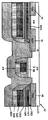
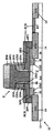
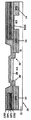
図2〜図29は、本発明によるデバイス10の製造プロセスを説明する断面図である。
2 to 29 are cross-sectional views illustrating the manufacturing process of the
図2は、製造プロセスの初期段階におけるデバイス10の断面図である。デバイス10は、通常の方法によって薄い熱酸化物層TOXで覆われたドープト・シリコン半導体基板11を有している。
Nドープト・コレクタ領域の形成
図3は、1組のリセスが基板11の表面に形成された後の図2のデバイス10を示す。リセスは、酸化シリコンよりなる浅いトレンチ分離(STI)領域14で充てんされている。STI領域14は、基板11内に形成されて、これらSTI領域間に、シリコン・アクティブ領域AA,コレクタ領域C,コレクタ・リーチスルー領域RTを画成している。アクティブ領域AAおよびリーチスルー領域RTは、STI領域14の間にある薄い熱酸化物層TOXの下側に配置されている。STI領域14は、PECVD,RTCVD,OZONE,TEOS,LPCVDを含むプロセスのグループから選ばれたプロセスによって形成されたあらゆる形態の酸化シリコンよりなる。NPNバイポーラ・トランジスタの場合、トランジスタのコレクタ領域Cを含むアクティブ領域AAは、当業者には明らかなように、N形ドーパントをイオン注入することにより、あるいはその場ドープト・エピタキシャル成長によって、ドープされる。
FIG. 2 is a cross-sectional view of
Formation of N-Doped Collector Region FIG. 3 shows the
図4は、窒化シリコンよりなる第1の薄い保護層SN1をブランケット付着し、続いてアクティブ領域から離れた位置に窓W1/W1′を有する第1のフォトレジスト・マスクPR1を形成して、シリコン基板11内のアクティブ領域AA上の窒化シリコンよりなる第1の薄い保護層SN1をパターニングするために用意した後の図3のデバイス10を示す。
FIG. 4 shows a blanket deposition of a first thin protective layer SN1 made of silicon nitride, followed by forming a first photoresist mask PR1 having windows W1 / W1 ′ away from the active area. FIG. 4 shows the
図5は、アクティブ領域AAから離れた位置にある、窒化シリコンよりなる薄い第1の保護層SN1の部分をエッチングして、アクティブ領域AAから離れた位置にある、STI領域14の表面の一部分と、リーチスルー領域RT上の熱酸化物とを露出させた後の図4のデバイス10を示す。第1のフォトレジスト・マスクPR1を除去して、窒化シリコンよりなる薄い第1の保護層SN1の一部分を、アクティブ領域AAおよび隣接するSTI領域14の一部分上に残す。
FIG. 5 shows a part of the surface of the
図6は、コンフォーマルな、酸化シリコンOX1よりなる薄膜と、アンドープト・ポリシリコンUP1と、第2の酸化シリコン層OX2とからなるスタックを付着した後に、中央窓W2を有する第2のパターニング・フォトレジスト・マスクPR2が形成された後の図5のデバイス10を示す。中央窓W2は、下側の第1の窒化シリコン層SN1の残りの部分のエッジを越えて、真性ベース領域のエピタキシャル成長に用いられる開口を形成している。
FIG. 6 shows a second patterning photo having a central window W2 after depositing a conformal stack of silicon oxide OX1, an undoped polysilicon UP1 and a second silicon oxide layer OX2. FIG. 6 shows the
図7は、第1の窒化シリコン層SN1上にある、露出している酸化シリコン層OX1/アンドープト・ポリシリコン層UP1/酸化シリコン層OX2のスタックを除去するRIEエッチング工程の後の図6のデバイス10を示す。次に、第2のフォトレジスト・マスクPR2を、デバイス10から除去する。
FIG. 7 shows the device of FIG. 6 after an RIE etching step that removes the exposed silicon oxide layer OX1 / undoped polysilicon layer UP1 / silicon oxide layer OX2 stack on the first silicon nitride layer SN1. 10 is shown. Next, the second photoresist mask PR2 is removed from the
図8は、第1の窒化シリコン層SN1を、ウェット・エッチャントすなわちホット・リン酸で除去し、熱酸化物層TOXおよび露出している第2の酸化シリコン層OX2を、ウェット・エッチャントすなわちHF酸でエッチング除去した後の図7のデバイス10を示す。
FIG. 8 shows the removal of the first silicon nitride layer SN1 with a wet etchant or hot phosphoric acid, and the thermal oxide layer TOX and the exposed second silicon oxide layer OX2 with a wet etchant or HF acid. FIG. 8 shows the
図9は、単結晶アクティブ領域AAの露出表面上に、真性ベース層IBをエピタキシャル成長し、同時に、STI領域14と、第1のアンドープト・ポリシリコン層UP1および第1の酸化シリコン層OX1よりなる残りのスタックとの上へ、第1のドープト多結晶シリコン層DPIを形成した後の図8のデバイス10を示す。真性ベース層IBとドープト・ポリシリコン層DP1とは、低温エピタキシ(LTE)により付着され、縦型トランジスタのコレクタ領域を有するアクティブ領域AA上に、Pドープされた結晶半導体シリコン(Si)またはシリコン・ゲルマニウム(Si−Ge)の真性ベース領域よりなるPドープト真性ベース層IBを形成する。また、シリコン基板11内のアクティブ領域AA上に、真性ベース層IBを付着するLTEプロセスは、第1のPドープト多結晶シリコン層DP1を同時に形成する。
FIG. 9 shows that the intrinsic base layer IB is epitaxially grown on the exposed surface of the single-crystal active area AA, and at the same time, the remaining comprising the
図10は、第3の酸化シリコン層OX3/第2のアンドープト・ポリシリコン層UP2/第2の窒化シリコン層SN2よりなるコンフォーマル層のスタックを、真性ベース層IBおよび第1のドープト・ポリシリコン層DP1を覆って、デバイス10上に付着した後の図9のデバイス10を示す。
FIG. 10 shows a stack of conformal layers consisting of the third silicon oxide layer OX3 / second undoped polysilicon layer UP2 / second silicon nitride layer SN2, the intrinsic base layer IB and the first doped polysilicon. FIG. 10 shows the
次に、エミッタ・ペデスタルEPが形成される(図11に示されているように)位置から離れた位置にある窓W3を有する第3のフォトレジスト・マスクPR3を、後の工程でエミッタ・ペデスタルEPおよび隆起外部ベース領域PERとを形成するために、パターニングする。 Next, a third photoresist mask PR3 having a window W3 at a position remote from the position where the emitter pedestal EP is to be formed (as shown in FIG. 11) is formed in a later step. Pattern to form EP and raised external base region PER .
図11は、第2の窒化シリコン層SN2およびアンドープト・ポリシリコン層UP2を含む図10において付加されたスタックの上部層を、マスクPR3内の窓W3を経てRIEエッチングした後の図10のデバイス10を示す。次に、第3のフォトレジスト・マスクPR3を除去する。アクティブ領域AA上の中央にあるエミッタ・ペデスタルEPの両側に、隆起外部ベース領域PERを形成する第3の酸化シリコン層OX3上で、エッチングは停止する。
FIG. 11 shows the
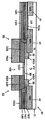
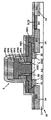
図12は、エミッタ・ペデスタルEPの側面、および隆起外部ベース領域PERから離れた位置にあるスタックの側面に、窒化シリコンよりなる側壁スペーサSN3を形成し、これにより第2の窒化シリコン層SN2およびアンドープト・ポリシリコン層UP2の露出側壁を覆った後の図11のデバイス10を示す
FIG. 12 shows the formation of sidewall spacers SN3 made of silicon nitride on the side of the emitter pedestal EP and on the side of the stack remote from the raised external base region PER , thereby forming the second silicon nitride layer SN2 and the undoped FIG. 11 shows the
図13は、酸化シリコン・スペーサOX4を形成して、図14,図15,図16に示される工程による分離エクステンション領域IEの形成に適合したエクステンション窓EWを、エミッタ・ペデスタルEPに対して自己整合で与えた後の図12のデバイス10を示す。即ち、側壁スペーサSN3と酸化シリコンスペーサOX4(これらを「側壁上のスペーサ」という)をマスクにしてエクステンション窓EW即ち分離エクステンション領域IEを形成する。スペーサOX4は、エクステンション窓EW内の露出ドープト・ポリシリコン層DP1をエッチングして、分離エクステンション領域IEおよび図14に示すようにドープト・シリコン層DPIがエッチング除去された分離エクステンション領域R1を形成するためにRIEを用いる際に、ハード・マスクとして用いられる。スペーサOX4の幅は、RIEの際にエミッタ・ペデスタルEPの周辺領域を画成して保護し、図16に示されるように、真性ベース層IBと外部ベース・ポリシリコン層DP2との間に、コンタクト領域を与える。
FIG. 13 shows the self-alignment of the extension window EW that is suitable for forming the isolation extension region IE according to the steps shown in FIGS. 14, 15, and 16 by forming the silicon oxide spacer OX4 with respect to the emitter pedestal EP. FIG. 13 shows the
図14は、ハードマスクとして酸化シリコン・スペーサOX4を用いて、露出真性ベース層IBとSTI上のドープト・ポリシリコン層DPIを経て、アクティブ領域AA内のコレクタ領域C内へエッチングして、スペーサOX4とエミッタ・ペデスタルEPに隣接する浅いトレンチ分離(STI)領域14との間のエミッタ・ペデスタルEPの周りに分離エクステンション・リセスR1を形成する。後のプロセスにおいて、酸化シリコンを、図16に示すように分離エクステンション・リセスR1に付着することによって、分離エクステンション領域IEが形成される。コレクタ領域C内に形成された分離エクステンション・リセスR1の幅および深さは、寄生容量を低減するように最適化される。さらに、アクティブ領域AA内のコレクタ領域C内の分離エクステンション・リセスR1は、最終のコレクタ構造を決定する。したがって、分離エクステンション・リセスR1の幅および深さは、当業者には明らかなように、コレクタ抵抗を調整するように最適化できる。
FIG. 14 shows etching using the silicon oxide spacer OX4 as a hard mask, through the exposed intrinsic base layer IB and the doped polysilicon layer DPI on the STI, and into the collector region C in the active region AA. And an isolation extension recess R1 is formed around the emitter pedestal EP between the emitter pedestal EP and the shallow trench isolation (STI)
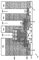
図15は、分離エクステンション・リセス(またはトレンチ)R1を充てんするように、コンフォーマル酸化シリコン層OX5を付着して、エミッタ・ペデスタルEPの周りへの分離エクステンション領域IEの形成を準備した後の図14のデバイス10を示す。
FIG. 15 is a view after preparing a formation of an isolation extension region IE around the emitter pedestal EP by depositing a conformal silicon oxide layer OX5 so as to fill the isolation extension recess (or trench) R1. 14
図16は、酸化物層OX5を平坦化し、真性ベース層IBまでエッチングまたはリセスして、分離エクステンション領域IEを形成した後の図15のデバイス10を示す。
FIG. 16 shows the
図13〜図16は、第1のエクステンション・トレンチ分離STI領域の形成とは独立に、浅い分離エクステンション領域IE(第2の浅い分離領域)が、いかに形成されるかを示している。分離エクステンション領域IE(第2の浅い分離領域)の形成のこの分離は、第1の浅いトレンチ分離STI領域が、バイポーラ・デバイスおよびCMOSデバイスの両方に共通ならば、ここで説明するバイポーラ・トランジスタが、BiCMOSを製造する通常のCMOSと両立することを可能にする。分離エクステンション領域IEの形成のこの分離は、また、分離エクステンション・リセスR1の深さと、第1の浅いトレンチ分離STI材料の誘電体特性とは異なる誘電体特性を有する異なる材料を用いるオプションとに対する調整により、ベース/コレクタ間寄生容量の低減を調整することを可能にする。例えば、酸化シリコン層OX5の代わりに低誘電率の異なる材料を用いて分離エクステンション・リセスR1を充てんして、寄生容量をさらに低減することができる。低誘電率を有するこのような材料は、SiLK,フッ化酸化物,多孔性酸化物を含むが、これらに限定されるものではない。 13 to 16 show how the shallow isolation extension region IE (second shallow isolation region) is formed independently of the formation of the first extension / trench isolation STI region. This isolation of the formation of the isolation extension region IE (second shallow isolation region) is achieved by the bipolar transistor described here if the first shallow trench isolation STI region is common to both bipolar and CMOS devices. This makes it possible to be compatible with a normal CMOS for manufacturing BiCMOS. This separation of the formation of the isolation extension region IE is also adjusted for the depth of the isolation extension recess R1 and the option of using different materials having different dielectric properties than the dielectric properties of the first shallow trench isolation STI material. This makes it possible to adjust the reduction of the base-collector parasitic capacitance. For example, the parasitic extension can be further reduced by filling the isolation extension recess R1 using a material having a low dielectric constant instead of the silicon oxide layer OX5. Such materials having a low dielectric constant include, but are not limited to, SiLK, fluoride oxide, and porous oxide.
図17は、ドープト・ポリシリコン層DP2を付着し、平坦化およびリセスして隆起外部ベース層DP2を形成した後の図16のデバイス10を示す。図17は、また、真性ベース層IBと外部ベース・ドープト・ポリシリコン層DP2との間の周辺コンタクト領域を示す。外部ベース領域は、図14に示される酸化シリコン・スペーサOX4によって画成され、保護されていた。
FIG. 17 shows the
図18は、分離酸化物OX6を付着し、分離酸化物OX6を平坦化およびリセスして、エミッタ・ペデスタルEPおよび層SN2/UP2のラテラル・スタックを露出させた後の図17のデバイス10を示す。
FIG. 18 shows the
図19は、窒化シリコン層SN2をRIEエッチングし、エミッタ・ペデスタルEPを除去して、分離スタックIS間にエミッタ開口EOを形成した後の図18のデバイス10を示す。分離スタックISは、分離酸化物OX6で覆われているドープト外部ベース・ポリシリコン層DP2のスタックで形成されている。窒化シリコン・スペーサSN3もRIEまたはウェット・エッチングで除去され、第3の酸化シリコン層OX3の上面が露出される。
FIG. 19 shows the
図20は、分離スタックISの側壁上に、最終の窒化シリコン・スペーサSN4を形成した後の図19のデバイス10を示す。
FIG. 20 shows the
図21は、エミッタ開口EOの底部およびフィールドにある第3の酸化シリコン層OX3の露出部分を除去し、真性ベース層IBの上面を露出させた後の図20のデバイス10を示す。
FIG. 21 shows the
図22は、ドープト・エミッタ・ポリシリコンDP3よりなるコンフォーマル層を付着し、ハードマスクHM′として働く窒化シリコンのコンフォーマル層を付着した後の図21のデバイス10を示す。パターニングされた第4のフォトレジスト・マスクPR4を、図23に示されるようにエミッタを形成するために用いられる層DP3/HM上に形成する。マスクPR4は、分離スタックISと重なる。
FIG. 22 shows the
図23は、窒化シリコン層HM′をエッチングして、ハードマスクHMを形成し、マスクPR4を除去した後の図22のデバイス10を示す。次に、ドープト・エミッタ・ポリシリコン層DP3,ドープト・ポリシリコン層DP1(窒化シリコン・スペーサSN4から離れた位置にある),アンドープト・ポリシリコン層UP1をRIEエッチングして、エミッタEを形成し、コレクタ・リーチスルー領域RTを露出させる。
FIG. 23 shows the
図24は、ドープト外部ベース・ポリシリコン層DP2上の分離酸化シリコン層OX6と、窒化シリコン・スペーサSN4の外側部分とを除去した後の図23のデバイス10を示す。
FIG. 24 shows the
図25は、エミッタ・スタックEの側壁上に窒化シリコン・スペーサSN5を形成した後の図24のデバイス10を示す。
FIG. 25 shows the
図26は、露出した外部ベース層DP2およびコレクタ・リーチスルー領域RT上にシリサイドSCDの層を形成した後の図25のデバイス10を示す。シリサイド層の形成は、ポリシリコン表面のシリサイド化技術の当業者には周知のプロセスによって行われる。
FIG. 26 shows the
図27は、デバイス全体上に窒化シリコン層SN6よりなる薄いコンフォーマル層を付着した後の図26のデバイス10を示す。
FIG. 27 shows the
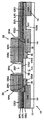
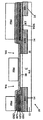
図28は、コンフォーマル窒化シリコン層SN6により覆われたデバイス10上に、酸化シリコンよりなる厚いブランケット層OX7を付着した後の図27のデバイス10を示す。酸化シリコン層OX7は、コンタクトを形成するために、平坦化されている。次に、フォトレジスト・マスクPR5のパターニングした層を、ビア・ホールVH1,VH2,VH3に対する開口を有して設ける。これらビア・ホールを介して、エミッタEへのコンタクトと、外部ベース層DP2上のベース・シリサイドSCDへのコンタクトと、基板11へのリーチスルーRTを経てコレクタ領域Cへのコンタクトとを形成する。ビアVH1〜VH3は、酸化シリコン層OX7をエッチングし、フォトレジストPR5を除去することによって形成される。
FIG. 28 shows the
図29は、コンフォーマル窒化シリコン層SN6と、エミッタ上の窒化シリコン・ハードマスクHMを、RIEエッチングし、金属層を付着し平坦化することによって、ビア金属コンタクトVI1,VI2,VI3を形成した後の図28のデバイス10を示す。
FIG. 29 shows the formation of via metal contacts VI1, VI2, VI3 by RIE etching the conformal silicon nitride layer SN6 and the silicon nitride hardmask HM on the emitter to deposit and planarize the metal layer. FIG. 29 shows the
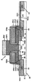
図30は、図29のデバイス10の変形であるデバイス10Aを示す。この構造は、次の点を除いて図29の構造と同じように作製される。すなわち、シリコン基板11のアクティブ領域AA内のコレクタ領域Cは、ウェットまたはRIE化学物質によってさらにエッチングされて、真性ベース領域IBのアンダーカットUCを形成する。これは、図2〜図29に示されるプロセスにおいて、アクティブ領域AA内のコレクタ領域Cをエッチングして、等方性エッチングで真性ベース領域IBの下側に達するアンダーカットUCを形成することによって、図14に示された工程で実現できる。このようなアンダーカットUCは、等方性RIEおよび/または次のようなエッチング化学物質を用いることによって実現できる。すなわち、エッチング化学物質は、ドーピング型,濃度,材料の種類に基づいて、アクティブ領域AA内のコレクタ領域Cと真性ベース領域IBとの間で高い選択性を有している。例えば、シリコン・ゲルマニウム(SiGe)ベースおよびシリコン・コレクタを有するヘテロ接合バイポーラ・トランジスタの場合に、シリコンはシリコン・ゲルマニウムに対して高いエッチング選択性を有する、水酸化アンモニウム(NH4OH)を含むウェット・エッチングを用いることができる。アクティブ領域AA内のコレクタ領域Cへの分離エクステンション・リセスR1の幅,深さ,アンダーカットは、寄生容量を低減するように最適化される。さらに、コレクタ領域C内の分離エクステンション・リセスR1は、最終のコレクタ構造を決定する。したがって、分離エクステンション・リセスR1の幅,深さ,アンダーカットを、当業者によって十分に理解されるように、最適化してコレクタ抵抗を調整することができる。
FIG. 30 shows a
図31は、図29のデバイス10の他の変形であるデバイス10Bを示す。この構造は、次の点を除いて図29の構造と同じように作製される。すなわち、図13において、真性ベース領域IBと、浅いトレンチ分離STI上のドープト・ポリシリコン層DP1との露出部分を酸化して、分離エクステンション領域IEを形成する。この場合、図13後の処理フロー工程は、図17にとぶ。
FIG. 31 shows a
図32〜図35は、図29および図30に示されるデバイス10および10Aを作製する際に非自己整合で浅い分離エクステンションIEを形成するための、図7〜図29に示されるプロセスの変形工程の断面図を示す。即ち、エミッタ・ペデスタルEPの側壁上のスペーサを用いないで分離エクステンション領域IEを形成する方法が示されている。マスクPR6を用いて、真性ベースIBの領域と、第1の浅いトレンチ分離上の第1のドープト・ポリシリコン層DP1とを、画成し露出させて、エミッタ・ペデスタルEPを形成する前に、分離エクステンション領域IEを形成する。図32および図33の処理工程は、図13〜図16の処理工程を置き換える。
FIGS. 32-35 are variations of the process shown in FIGS. 7-29 for forming a non-self-aligned shallow isolation extension IE in making the
図32は、デバイス10上に真性ベース層IBおよび第1のドープト・ポリシリコン層DP1を覆うように、酸化シリコン層OX3を付着した後の図9のデバイス10を示す。次に、窓W6を有するフォトレジスト・マスクPR6をパターニングして、後の工程で分離エクステンション領域IEを形成する。
FIG. 32 shows the
図33は、マスクPR6内の窓W6を経て、酸化シリコン層OX3にRIEエッチングを行い、エクステンション窓EW′を形成した後の図32のデバイス10を示す。エッチングは、真性ベース層IBの領域上で停止し、真性ベース層IBの右エッジおよび左エッジ、および第1のドープト・ポリシリコン層を露出させる。この第1のドープト・ポリシリコン層DP1は、分離エクステンションIEを形成するために、RIEエッチングされる。次に、フォトレジスト・マスクPR6を除去する。エクステンション窓EW′の内側の酸化シリコン層OX3の幅は、エミッタ・ペデスタルEPの領域とエミッタ・ペデスタルEPの周辺領域とを画成し保護して、RIEエッチングの際に、真性ベース層IBと外部ベース・ポリシリコン層DP2との間に、コンタクト領域を与える(図17に示す)。
FIG. 33 shows the
図34は、露出した真性ベース層34とSTI上のドープト・ポリシリコンDP1を、酸化シリコン層OX3をハードマスクとして用いて、アクティブ領域AA内のコレクタ領域CにまでRIEエッチングした後の図33のデバイス10を示す。RIEエッチングは、真性ベース層IBと浅いトレンチ分離STIとの間に、分離エクステンション・リセスR1′を形成する。
34 shows the exposed intrinsic base layer 34 and doped polysilicon DP1 on the STI after RIE etching to the collector region C in the active region AA using the silicon oxide layer OX3 as a hard mask.
図35は、酸化シリコン層OX3をウェット・エッチングで除去し、コンフォーマル酸化シリコン層OX5を付着して、分離エクステンション・リセス(またはトレンチ)R1′を充てんして、分離エクステンション領域IE′を形成した後の図34のデバイス10を示す。次に、処理フローは、図10の工程から進み、図13〜図16の工程をとばして、図29および図30に示すデバイス10および10Aを作製する。
In FIG. 35, the silicon oxide layer OX3 is removed by wet etching, the conformal silicon oxide layer OX5 is deposited, and the isolation extension recess (or trench) R1 ′ is filled to form the isolation extension region IE ′. FIG. 35 shows the
図36〜図38は、図32に示したものと同じマスクPR6を用いて、図31に示されたデバイス10Bを作製する際に非自己整合で浅い分離エクステンションIEを形成するための、図32〜図35に示されるプロセスの変形の断面図を示す。即ち、エミッタ・ペデスタルEPの側壁上のスペーサを用いないで分離エクステンション領域IEを形成する方法が示されている。マスクPR6を用いて、真性ベースIBの領域と、第1の浅いトレンチ分離上の第1のドープト・ポリシリコンDP1とを画成し露出させて、エミッタ・ペデスタルEPを形成する前に、分離エクステンション領域IEを形成する。図36〜図38の処理工程は、図13〜図16の処理工程を置き換える。
FIGS. 36 to 38 are views for forming a non-self-aligned shallow isolation extension IE when manufacturing the
図36は、デバイス10上に真性ベースIBおよび第1のドープト・ポリシリコン層DP1を覆うように、酸化シリコン層OX3を付着した後の図9のデバイス10を示す。次に、窓W6を有するフォトレジスト・マスクPR6をパターニングして、続く工程で分離エクステンション領域IEを形成する。
FIG. 36 shows the
図37は、マスクPR6内の窓W6を経て、酸化シリコン層OX3にRIEエッチングを行い、エクステンション窓EW′を形成した後の図36のデバイス10を示す。エッチングは、真性ベース層IBおよび第1のドープト・ポリシリコン層DP1の領域上で停止し、酸化して分離エクステンションIEを形成する。次に、フォトレジスト・マスクPR6を除去する。エクステンション窓EW′の内側の酸化シリコン層OX3の幅は、エミッタ・ペデスタルEPの領域とエミッタ・ペデスタルEPの周辺領域とを画成し保護して、RIEエッチングの際に、真性ベース層IBと外部ベース・ポリシリコン層DP2との間に、コンタクト領域を与える(図17に示す)。
FIG. 37 shows the
図38は、図37の真性ベース装置IBの露出領域と浅いトレンチ分離STI上のドープト・ポリシリコンDP1を酸化して、分離エクステンション領域IE′を形成した後の図37のデバイス10を示す。次に、処理フローは、図10の工程から進み、図13〜図16の工程をとばして、図31に示したデバイス10Bを作製する。
FIG. 38 shows the
本発明を、特定の実施例によって説明したが、当業者であれば、本発明の趣旨および範囲内で変更して本発明を実施できることがわかるであろう。すなわち、変更は本発明の趣旨および範囲内を逸脱することなしに好適かつ詳細に行うことができる。したがって、このようなすべての変更は、本発明の範囲内にある。 While the invention has been described in terms of specific embodiments, those skilled in the art will recognize that the invention can be practiced with modification within the spirit and scope of the invention. That is, changes can be made suitably and in detail without departing from the spirit and scope of the present invention. Accordingly, all such modifications are within the scope of the present invention.
まとめとして、本発明の構成に関して以下の事項を開示する。
(1)シリコン半導体基板内に形成された縦型バイポーラ・トランジスタであって、
上面を有する前記基板と、
前記基板内に形成され、誘電体材料よりなり内側端部と上面とを有する浅いトレンチ分離(STI)領域と、
前記基板内であって、1対の前記STI領域の間に形成されたドープト・コレクタ領域と、
前記基板の上面であって、前記1対のSTI領域の間に形成されたカウンタドープト・真性ベース領域とを備え、前記真性ベース領域と前記1対のSTI領域との間にマージンがあり、前記真性ベース領域はエッジを有し、
前記真性ベース領域上に、前記エッジから離れて形成されたドープト・エミッタ領域と、
前記STI領域と前記真性ベース領域との間の前記マージン内に形成され、前記真性ベース領域の前記エッジと並置された誘電体材料よりなる浅い分離エクステンション領域と、
前記浅い分離エクステンション領域を覆い、前記真性ベース領域上に部分的に延びて物理的および電気的に接触する外部ベース領域とを備えた縦型バイポーラ・トランジスタ。
(2)前記浅い分離エクステンション領域は、前記エミッタに整合されている、上記(1)に記載の縦型バイポーラ・トランジスタ。
(3)前記浅い分離エクステンション領域は、前記エミッタに整合されていない、上記(1)に記載の縦型バイポーラ・トランジスタ。
(4)前記浅い分離エクステンション領域は、酸化されたドープト・シリコンと付着された酸化シリコンとよりなるグループから選択された酸化物材料で形成されている、上記(1)に記載の縦型バイポーラ・トランジスタ。
(5)前記浅い分離エクステンション領域は、前記STI領域よりも低い誘電率を有する材料で形成されている、上記(1)に記載の縦型バイポーラ・トランジスタ。
(6)前記浅い分離エクステンション領域は、前記STI領域の前記内側端部および前記上面に重なっている、上記(1)に記載の縦型バイポーラ・トランジスタ。
(7)前記浅い分離エクステンション領域は、前記真性ベース領域のエッジの下に延びている、上記(1)に記載の縦型バイポーラ・トランジスタ。
(8)前記真性ベース領域は、ドープト多結晶シリコンおよびシリコン・ゲルマニウムよりなるグループから選択された材料よりなる、上記(1)に記載の縦型バイポーラ・トランジスタ。
(9)前記浅い分離エクステンション領域は、ドープト・コレクタ領域内に延びて、ドープト・コレクタ領域の抵抗を変化させる、上記(1)に記載の縦型バイポーラ・トランジスタ。
(10)シリコン半導体基板内に形成された縦型バイポーラ・トランジスタであって、
上面を有する前記基板と、
前記基板内に形成され、誘電体材料よりなり内側端部と上面とを有する浅いトレンチ分離(STI)領域と、
前記基板内であって、1対の前記STI領域の間に形成されたドープト・コレクタ領域と、
前記基板の上面であって、前記1対のSTI領域の間に形成されたカウンタドープト・真性ベース領域とを備え、前記真性ベース領域と前記1対のSTI領域との間にマージンがあり、前記真性ベース領域はエッジを有し、
前記真性ベース領域は、ドープト多結晶シリコンおよびシリコン・ゲルマニウムよりなるグループから選択された材料よりなり、
前記真性ベース領域上に、前記エッジから離れて、ドープト・ポリシリコンで形成されたドープト・エミッタ領域と、
前記STI領域と前記真性ベース領域との間の前記マージン内に形成され、前記真性ベース領域の前記エッジと並置された誘電体材料よりなり、前記STI領域の前記内側端部および上面を覆う浅い分離エクステンション領域と、
前記浅い分離エクステンション領域を覆い、前記真性ベース領域上に部分的に延びて物理的および電気的に接触する外部ベース領域と、
前記エミッタ領域上に形成された窒化シリコン・キャップおよび前記エミッタ領域の側壁上に形成された窒化シリコン側壁スペーサとを備えた縦型バイポーラ・トランジスタ。
(11)前記浅い分離エクステンション領域は、前記エミッタに整合されている、上記(10)に記載の縦型バイポーラ・トランジスタ。
(12)前記浅い分離エクステンション領域は、前記エミッタに整合されていない、上記(10)に記載の縦型バイポーラ・トランジスタ。
(13)前記浅い分離エクステンション領域は、前記基板の酸化物で形成されている、上記(10)に記載の縦型バイポーラ・トランジスタ。
(14)前記浅い分離エクステンション領域は、前記STI領域よりも低い誘電率を有する材料で形成されている、上記(10)に記載の縦型バイポーラ・トランジスタ。
(15)前記浅い分離エクステンション領域は、前記真性ベース領域のエッジの下に延びている、上記(10)に記載の縦型バイポーラ・トランジスタ。
(16)上面を有するシリコン半導体基板内に形成された縦型バイポーラ・トランジスタの製造方法であって、
前記基板内に形成され、誘電体材料よりなり内側端部と上面とを有する浅いトレンチ分離(STI)領域を形成する工程と、
前記基板内であって、1対の前記STI領域の間に形成されたドープト・コレクタ領域を形成する工程と、
前記基板の上面であって、前記1対のSTI領域の間に形成されたカウンタドープト・真性ベース領域を形成する工程とを含み、前記真性ベース領域と前記1対のSTI領域との間にマージンがあり、前記真性ベース領域はエッジを有し、
前記真性ベース領域上に、前記エッジから離れて形成されたドープト・エミッタ領域を形成する工程と、
前記STI領域と前記真性ベース領域との間の前記マージン内に形成され、前記真性ベース領域の前記エッジと並置された誘電体材料よりなる浅い分離エクステンション領域を形成する工程と、
前記浅い分離エクステンション領域を覆い、前記真性ベース領域上に部分的に延びて物理的および電気的に接触する外部ベース領域を形成する工程とを含む縦型バイポーラ・トランジスタの製造方法。
(17)前記浅い分離エクステンション領域を、酸化またはRIEよりなるグループより選択された方法によって形成し、分離エクステンション・リセスを形成し、この分離エクステンション・リセスを誘電体材料で充てんする、上記(16)に記載の方法。
(18)前記浅い分離エクステンション領域は、前記エミッタに整合されている、上記(16)に記載の方法。
(19)前記浅い分離エクステンション領域は、前記エミッタに整合されていない、上記(16)に記載の方法。
(20)前記STI領域の前記内側端部および前記上面に重ねて、前記浅い分離エクステンション領域を形成する工程と、
前記基板上に熱酸化物層を形成する工程と、
アクティブ領域を画成する前記基板内の浅いトレンチ分離(STI)領域と、このアクティブ領域から離れた位置にあるコレクタ・リーチスルー領域とを形成する工程と、
前記アクティブ領域の上に第1の窒化シリコン層を形成する工程と、
前記第1の窒化シリコン層から離れた位置に、第1の酸化シリコン層と、第1のアンドープト・ポリシリコン層と、第2の酸化シリコン層とからなるスタックを形成し、前記コレクタ・リーチスルー領域を覆い、前記STI領域を部分的に覆う工程と、
前記第1の窒化シリコン層を除去する工程と、
前記アクティブ領域上に真性ベース・エピタキシャル層を形成する工程と、
第3の酸化シリコン層と、第2のアンドープト・ポリシリコン層と、第2の窒化シリコン層とからなる犠牲エミッタ・スタックを、前記犠牲エミッタ・スタックの各側面に露出部分を残して、前記アクティブ領域の部分上の中央に形成する工程とを含む、上記(16)に記載の方法。
In summary, the following matters are disclosed regarding the configuration of the present invention.
(1) A vertical bipolar transistor formed in a silicon semiconductor substrate,
The substrate having an upper surface;
A shallow trench isolation (STI) region formed in the substrate and made of a dielectric material and having an inner end and an upper surface;
A doped collector region formed in the substrate and between the pair of the STI regions;
A counter-doped intrinsic base region formed on the upper surface of the substrate and between the pair of STI regions, with a margin between the intrinsic base region and the pair of STI regions; The intrinsic base region has edges;
A doped emitter region formed on the intrinsic base region away from the edge;
A shallow isolation extension region formed of a dielectric material formed within the margin between the STI region and the intrinsic base region and juxtaposed with the edge of the intrinsic base region;
A vertical bipolar transistor that covers the shallow isolation extension region and includes an external base region that extends partially over the intrinsic base region and is in physical and electrical contact.
(2) The vertical bipolar transistor according to (1), wherein the shallow isolation extension region is aligned with the emitter.
(3) The vertical bipolar transistor according to (1), wherein the shallow isolation extension region is not aligned with the emitter.
(4) The vertical bipolar region according to (1), wherein the shallow isolation extension region is formed of an oxide material selected from the group consisting of oxidized doped silicon and deposited silicon oxide. Transistor.
(5) The vertical bipolar transistor according to (1), wherein the shallow isolation extension region is formed of a material having a dielectric constant lower than that of the STI region.
(6) The vertical bipolar transistor according to (1), wherein the shallow isolation extension region overlaps the inner end portion and the upper surface of the STI region.
(7) The vertical bipolar transistor according to (1), wherein the shallow isolation extension region extends under an edge of the intrinsic base region.
(8) The vertical bipolar transistor according to (1), wherein the intrinsic base region is made of a material selected from the group consisting of doped polycrystalline silicon and silicon germanium.
(9) The vertical bipolar transistor according to (1), wherein the shallow isolation extension region extends into the doped collector region to change the resistance of the doped collector region.
(10) A vertical bipolar transistor formed in a silicon semiconductor substrate,
The substrate having an upper surface;
A shallow trench isolation (STI) region formed in the substrate and made of a dielectric material and having an inner end and an upper surface;
A doped collector region formed in the substrate and between the pair of the STI regions;
A counter-doped intrinsic base region formed on the upper surface of the substrate and between the pair of STI regions, with a margin between the intrinsic base region and the pair of STI regions; The intrinsic base region has edges;
The intrinsic base region is made of a material selected from the group consisting of doped polycrystalline silicon and silicon germanium;
On the intrinsic base region, away from the edge, a doped emitter region formed of doped polysilicon;
Shallow isolation formed in the margin between the STI region and the intrinsic base region and made of a dielectric material juxtaposed with the edge of the intrinsic base region and covering the inner end and top surface of the STI region An extension area;
An outer base region covering the shallow isolation extension region and partially extending over the intrinsic base region and in physical and electrical contact;
A vertical bipolar transistor comprising a silicon nitride cap formed on the emitter region and a silicon nitride sidewall spacer formed on a sidewall of the emitter region.
(11) The vertical bipolar transistor according to (10), wherein the shallow isolation extension region is aligned with the emitter.
(12) The vertical bipolar transistor according to (10), wherein the shallow isolation extension region is not aligned with the emitter.
(13) The vertical bipolar transistor according to (10), wherein the shallow isolation extension region is formed of an oxide of the substrate.
(14) The vertical bipolar transistor according to (10), wherein the shallow isolation extension region is formed of a material having a dielectric constant lower than that of the STI region.
(15) The vertical bipolar transistor according to (10), wherein the shallow isolation extension region extends under an edge of the intrinsic base region.
(16) A method of manufacturing a vertical bipolar transistor formed in a silicon semiconductor substrate having an upper surface,
Forming a shallow trench isolation (STI) region formed in the substrate and made of a dielectric material and having an inner end and an upper surface;
Forming a doped collector region formed in the substrate and between the pair of the STI regions;
Forming a counter-doped intrinsic base region formed between the pair of STI regions on the top surface of the substrate, the method comprising: forming a counter-doped intrinsic base region between the pair of STI regions; There is a margin, the intrinsic base region has an edge;
Forming a doped emitter region formed away from the edge on the intrinsic base region;
Forming a shallow isolation extension region made of a dielectric material formed within the margin between the STI region and the intrinsic base region and juxtaposed with the edge of the intrinsic base region;
And forming an external base region that covers the shallow isolation extension region and extends partially over the intrinsic base region to make physical and electrical contact therewith.
(17) The shallow isolation extension region is formed by a method selected from the group consisting of oxidation or RIE, an isolation extension recess is formed, and the isolation extension recess is filled with a dielectric material. The method described in 1.
(18) The method according to (16), wherein the shallow isolation extension region is aligned with the emitter.
(19) The method according to (16), wherein the shallow isolation extension region is not aligned with the emitter.
(20) forming the shallow isolation extension region overlying the inner end of the STI region and the upper surface;
Forming a thermal oxide layer on the substrate;
Forming a shallow trench isolation (STI) region in the substrate that defines an active region, and a collector reach-through region remote from the active region;
Forming a first silicon nitride layer on the active region;
A stack comprising a first silicon oxide layer, a first undoped polysilicon layer, and a second silicon oxide layer is formed at a position away from the first silicon nitride layer, and the collector reach through Covering the region and partially covering the STI region;
Removing the first silicon nitride layer;
Forming an intrinsic base epitaxial layer on the active region;
A sacrificial emitter stack comprising a third silicon oxide layer, a second undoped polysilicon layer, and a second silicon nitride layer is formed on the active side of the sacrificial emitter stack, leaving an exposed portion on each side. Forming in the center on a portion of the region.
10 デバイス
11 基板
14 浅いトレンチ分離(STI)領域14
AA アクティブ領域
C コレクタ領域
DP ドープト・ポリシリコン層
EP エミッタ・ペデスタル
EW エクステンション窓
IB 真性ベース層
IE 分離エクステンション領域
IS 分離スタック
OX 酸化シリコン層
PER 隆起外部ベース領域
PR フォトレジスト・マスク
R1 分離エクステンション・リセス
RT リーチスルー領域
SN 窒化シリコン層
UP アンドープト・ポリシリコン層
W 窓
10
AA active region C collector region DP doped polysilicon layer EP emitter pedestal EW extension window IB intrinsic base layer IE isolation extension region IS isolation stack OX silicon oxide layer PER raised external base region PR photoresist mask R1 isolation extension recess RT Reach-through area SN Silicon nitride layer UP Undoped polysilicon layer W Window
Claims (7)
上面を有する前記基板と、
前記基板内に形成され、誘電体材料よりなり内側端部と上面とを有する浅いトレンチ分離(STI)領域と、
前記基板内であって、1対の前記STI領域の間に形成されたドープト・コレクタ領域と、
前記基板の上面であって、前記1対のSTI領域の間に形成されたカウンタドープト・真性ベース領域とを備え、前記真性ベース領域と前記1対のSTI領域との間にマージンがあり、前記真性ベース領域はエッジを有し、
前記真性ベース領域上に、前記エッジから離れて形成されたドープト・エミッタ領域と、
前記STI領域と前記真性ベース領域との間の前記マージン内に形成され、前記真性ベース領域の前記エッジと並置された誘電体材料よりなる浅い分離エクステンション領域と、
前記浅い分離エクステンション領域を覆い、前記真性ベース領域上に部分的に延びて物理的および電気的に接触する外部ベース領域とを備え、前記浅い分離エクステンション領域は、前記STI領域よりも低い誘電率を有する材料で形成されている、縦型バイポーラ・トランジスタ。 A vertical bipolar transistor formed in a silicon semiconductor substrate,
The substrate having an upper surface;
A shallow trench isolation (STI) region formed in the substrate and made of a dielectric material and having an inner end and an upper surface;
A doped collector region formed in the substrate and between the pair of the STI regions;
A counter-doped intrinsic base region formed on the upper surface of the substrate and between the pair of STI regions, with a margin between the intrinsic base region and the pair of STI regions; The intrinsic base region has edges;
A doped emitter region formed on the intrinsic base region away from the edge;
A shallow isolation extension region formed of a dielectric material formed within the margin between the STI region and the intrinsic base region and juxtaposed with the edge of the intrinsic base region;
An outer base region that covers the shallow isolation extension region and extends partially over the intrinsic base region and is in physical and electrical contact, wherein the shallow isolation extension region has a lower dielectric constant than the STI region. A vertical bipolar transistor formed of a material having the same.
上面を有する前記基板と、
前記基板内に形成され、誘電体材料よりなり内側端部と上面とを有する浅いトレンチ分離(STI)領域と、
前記基板内であって、1対の前記STI領域の間に形成されたドープト・コレクタ領域と、
前記基板の上面であって、前記1対のSTI領域の間に形成されたカウンタドープト・真性ベース領域とを備え、前記真性ベース領域と前記1対のSTI領域との間にマージンがあり、前記真性ベース領域はエッジを有し、
前記真性ベース領域上に、前記エッジから離れて形成されたドープト・エミッタ領域と、
前記STI領域と前記真性ベース領域との間の前記マージン内に形成され、前記真性ベース領域の前記エッジと並置された誘電体材料よりなる浅い分離エクステンション領域と、
前記浅い分離エクステンション領域を覆い、前記真性ベース領域上に部分的に延びて物理的および電気的に接触する外部ベース領域とを備え、前記浅い分離エクステンション領域は、前記STI領域の前記内側端部および前記上面に重なっている、縦型バイポーラ・トランジスタ。 A vertical bipolar transistor formed in a silicon semiconductor substrate,
The substrate having an upper surface;
A shallow trench isolation (STI) region formed in the substrate and made of a dielectric material and having an inner end and an upper surface;
A doped collector region formed in the substrate and between the pair of the STI regions;
A counter-doped intrinsic base region formed on the upper surface of the substrate and between the pair of STI regions, with a margin between the intrinsic base region and the pair of STI regions; The intrinsic base region has edges;
A doped emitter region formed on the intrinsic base region away from the edge;
A shallow isolation extension region formed of a dielectric material formed within the margin between the STI region and the intrinsic base region and juxtaposed with the edge of the intrinsic base region;
An outer base region covering the shallow isolation extension region and partially extending over the intrinsic base region and in physical and electrical contact, wherein the shallow isolation extension region includes the inner end of the STI region and A vertical bipolar transistor overlying the top surface.
上面を有する前記基板と、
前記基板内に形成され、誘電体材料よりなり内側端部と上面とを有する浅いトレンチ分離(STI)領域と、
前記基板内であって、1対の前記STI領域の間に形成されたドープト・コレクタ領域と、
前記基板の上面であって、前記1対のSTI領域の間に形成されたカウンタドープト・真性ベース領域とを備え、前記真性ベース領域と前記1対のSTI領域との間にマージンがあり、前記真性ベース領域はエッジを有し、
前記真性ベース領域上に、前記エッジから離れて形成されたドープト・エミッタ領域と、
前記STI領域と前記真性ベース領域との間の前記マージン内に形成され、前記真性ベース領域の前記エッジと並置された誘電体材料よりなる浅い分離エクステンション領域と、
前記浅い分離エクステンション領域を覆い、前記真性ベース領域上に部分的に延びて物理的および電気的に接触する外部ベース領域とを備え、前記浅い分離エクステンション領域は、前記真性ベース領域のエッジの下に延びている縦型バイポーラ・トランジスタ。 A vertical bipolar transistor formed in a silicon semiconductor substrate,
The substrate having an upper surface;
A shallow trench isolation (STI) region formed in the substrate and made of a dielectric material and having an inner end and an upper surface;
A doped collector region formed in the substrate and between the pair of the STI regions;
A counter-doped intrinsic base region formed on the upper surface of the substrate and between the pair of STI regions, with a margin between the intrinsic base region and the pair of STI regions; The intrinsic base region has edges;
A doped emitter region formed on the intrinsic base region away from the edge;
A shallow isolation extension region formed of a dielectric material formed within the margin between the STI region and the intrinsic base region and juxtaposed with the edge of the intrinsic base region;
An outer base region covering the shallow isolation extension region and partially extending over the intrinsic base region and in physical and electrical contact, the shallow isolation extension region under the edge of the intrinsic base region An extending vertical bipolar transistor.
上面を有する前記基板と、
前記基板内に形成され、誘電体材料よりなり内側端部と上面とを有する浅いトレンチ分離(STI)領域と、
前記基板内であって、1対の前記STI領域の間に形成されたドープト・コレクタ領域と、
前記基板の上面であって、前記1対のSTI領域の間に形成されたカウンタドープト・真性ベース領域とを備え、前記真性ベース領域と前記1対のSTI領域との間にマージンがあり、前記真性ベース領域はエッジを有し、
前記真性ベース領域は、ドープト多結晶シリコンおよびシリコン・ゲルマニウムよりなるグループから選択された材料よりなり、
前記真性ベース領域上に、前記エッジから離れて、ドープト・ポリシリコンで形成されたドープト・エミッタ領域と、
前記STI領域と前記真性ベース領域との間の前記マージン内に形成され、前記真性ベース領域の前記エッジと並置された誘電体材料よりなり、前記STI領域の前記内側端部および上面を覆う浅い分離エクステンション領域と、
前記浅い分離エクステンション領域を覆い、前記真性ベース領域上に部分的に延びて物理的および電気的に接触する外部ベース領域と、
前記エミッタ領域上に形成された窒化シリコン・キャップおよび前記エミッタ領域の側壁上に形成された窒化シリコン側壁スペーサとを備えた縦型バイポーラ・トランジスタ。 A vertical bipolar transistor formed in a silicon semiconductor substrate,
The substrate having an upper surface;
A shallow trench isolation (STI) region formed in the substrate and made of a dielectric material and having an inner end and an upper surface;
A doped collector region formed in the substrate and between the pair of the STI regions;
A counter-doped intrinsic base region formed on the upper surface of the substrate and between the pair of STI regions, with a margin between the intrinsic base region and the pair of STI regions; The intrinsic base region has edges;
The intrinsic base region is made of a material selected from the group consisting of doped polycrystalline silicon and silicon germanium;
On the intrinsic base region, away from the edge, a doped emitter region formed of doped polysilicon;
Shallow isolation formed in the margin between the STI region and the intrinsic base region and made of a dielectric material juxtaposed with the edge of the intrinsic base region and covering the inner end and top surface of the STI region An extension area;
An outer base region covering the shallow isolation extension region and partially extending over the intrinsic base region and in physical and electrical contact;
A vertical bipolar transistor comprising a silicon nitride cap formed on the emitter region and a silicon nitride sidewall spacer formed on a sidewall of the emitter region.
Applications Claiming Priority (1)
| Application Number | Priority Date | Filing Date | Title |
|---|---|---|---|
| US10/249,299 US6864560B2 (en) | 2003-03-28 | 2003-03-28 | Bipolar transistor structure with a shallow isolation extension region providing reduced parasitic capacitance |
Publications (2)
| Publication Number | Publication Date |
|---|---|
| JP2004304190A JP2004304190A (en) | 2004-10-28 |
| JP4170246B2 true JP4170246B2 (en) | 2008-10-22 |
Family
ID=32987050
Family Applications (1)
| Application Number | Title | Priority Date | Filing Date |
|---|---|---|---|
| JP2004090598A Expired - Fee Related JP4170246B2 (en) | 2003-03-28 | 2004-03-25 | Vertical bipolar transistor |
Country Status (4)
| Country | Link |
|---|---|
| US (1) | US6864560B2 (en) |
| JP (1) | JP4170246B2 (en) |
| KR (1) | KR100637778B1 (en) |
| TW (1) | TWI267164B (en) |
Families Citing this family (38)
| Publication number | Priority date | Publication date | Assignee | Title |
|---|---|---|---|---|
| US7372091B2 (en) * | 2004-01-27 | 2008-05-13 | Micron Technology, Inc. | Selective epitaxy vertical integrated circuit components |
| US7087940B2 (en) * | 2004-04-22 | 2006-08-08 | International Business Machines Corporation | Structure and method of forming bipolar transistor having a self-aligned raised extrinsic base using self-aligned etch stop layer |
| US7118995B2 (en) * | 2004-05-19 | 2006-10-10 | International Business Machines Corporation | Yield improvement in silicon-germanium epitaxial growth |
| US7504685B2 (en) | 2005-06-28 | 2009-03-17 | Micron Technology, Inc. | Oxide epitaxial isolation |
| US20070023864A1 (en) * | 2005-07-28 | 2007-02-01 | International Business Machines Corporation | Methods of fabricating bipolar transistor for improved isolation, passivation and critical dimension control |
| US7342293B2 (en) * | 2005-12-05 | 2008-03-11 | International Business Machines Corporation | Bipolar junction transistors (BJTS) with second shallow trench isolation (STI) regions, and methods for forming same |
| TW200809980A (en) * | 2006-03-10 | 2008-02-16 | Koninkl Philips Electronics Nv | Method of manufacturing a bipolar transistor |
| US7888745B2 (en) | 2006-06-21 | 2011-02-15 | International Business Machines Corporation | Bipolar transistor with dual shallow trench isolation and low base resistance |
| US7521772B2 (en) * | 2006-11-08 | 2009-04-21 | International Business Machines Corporation | Monocrystalline extrinsic base and emitter heterojunction bipolar transistor and related methods |
| US7952165B2 (en) * | 2007-01-10 | 2011-05-31 | International Business Machines Corporation | Heterojunction bipolar transistor (HBT) with self-aligned sub-lithographic metal-semiconductor alloy base contacts |
| US7892910B2 (en) * | 2007-02-28 | 2011-02-22 | International Business Machines Corporation | Bipolar transistor with raised extrinsic self-aligned base using selective epitaxial growth for BiCMOS integration |
| US7927958B1 (en) * | 2007-05-15 | 2011-04-19 | National Semiconductor Corporation | System and method for providing a self aligned bipolar transistor using a silicon nitride ring |
| KR100983711B1 (en) * | 2008-08-29 | 2010-09-24 | 주식회사 하이닉스반도체 | Method for forming semiconductor device |
| CN102403222B (en) * | 2010-09-09 | 2013-09-11 | 上海华虹Nec电子有限公司 | Manufacturing method for silicon germanium heterojunction bipolar transistors |
| US20120313146A1 (en) * | 2011-06-08 | 2012-12-13 | International Business Machines Corporation | Transistor and method of forming the transistor so as to have reduced base resistance |
| US8536012B2 (en) | 2011-07-06 | 2013-09-17 | International Business Machines Corporation | Bipolar junction transistors with a link region connecting the intrinsic and extrinsic bases |
| US8916446B2 (en) * | 2011-11-11 | 2014-12-23 | International Business Machines Corporation | Bipolar junction transistor with multiple emitter fingers |
| US8546230B2 (en) * | 2011-11-15 | 2013-10-01 | International Business Machines Corporation | Bipolar transistor with a collector having a protected outer edge portion for reduced based-collector junction capacitance and a method of forming the transistor |
| US9093491B2 (en) | 2012-12-05 | 2015-07-28 | International Business Machines Corporation | Bipolar junction transistors with reduced base-collector junction capacitance |
| CN103022109B (en) * | 2012-12-20 | 2015-02-04 | 清华大学 | Bipolar transistor with fully self-alignment local oxidized lifting outer base region and preparation method of bipolar transistor |
| US8956945B2 (en) | 2013-02-04 | 2015-02-17 | International Business Machines Corporation | Trench isolation for bipolar junction transistors in BiCMOS technology |
| US8796149B1 (en) | 2013-02-18 | 2014-08-05 | International Business Machines Corporation | Collector-up bipolar junction transistors in BiCMOS technology |
| US8927381B2 (en) | 2013-03-20 | 2015-01-06 | International Business Machines Corporation | Self-aligned bipolar junction transistors |
| US8975146B2 (en) | 2013-05-01 | 2015-03-10 | International Business Machines Corporation | Trench isolation structures and methods for bipolar junction transistors |
| US8999804B2 (en) * | 2013-05-06 | 2015-04-07 | International Business Machines Corporation | Methods for fabricating a bipolar junction transistor with self-aligned terminals |
| US9059234B2 (en) | 2013-10-22 | 2015-06-16 | International Business Machines Corporation | Formation of a high aspect ratio trench in a semiconductor substrate and a bipolar semiconductor device having a high aspect ratio trench isolation region |
| US10468484B2 (en) * | 2014-05-21 | 2019-11-05 | Analog Devices Global | Bipolar transistor |
| US9666709B2 (en) * | 2015-01-29 | 2017-05-30 | Globalfoundries Inc. | Non-planar semiconductor structure with preserved isolation region |
| US9831328B2 (en) * | 2015-02-12 | 2017-11-28 | Taiwan Semiconductor Manufacturing Co., Ltd. | Bipolar junction transistor (BJT) base conductor pullback |
| US9722057B2 (en) | 2015-06-23 | 2017-08-01 | Global Foundries Inc. | Bipolar junction transistors with a buried dielectric region in the active device region |
| US10431654B2 (en) * | 2015-06-25 | 2019-10-01 | International Business Machines Corporation | Extrinsic base doping for bipolar junction transistors |
| US9368608B1 (en) | 2015-06-25 | 2016-06-14 | Globalfoundries Inc. | Heterojunction bipolar transistor with improved performance and breakdown voltage |
| US9812447B2 (en) | 2016-02-02 | 2017-11-07 | Globalfoundries Inc. | Bipolar junction transistors with extrinsic device regions free of trench isolation |
| US10319716B2 (en) * | 2017-05-05 | 2019-06-11 | Newport Fab, Llc | Substrate isolation for low-loss radio frequency (RF) circuits |
| US10290631B2 (en) * | 2017-05-05 | 2019-05-14 | Newport Fab, Llc | Linearity and lateral isolation in a BiCMOS process through counter-doping of epitaxial silicon region |
| US11152265B2 (en) | 2019-08-01 | 2021-10-19 | International Business Machines Corporation | Local isolation of source/drain for reducing parasitic capacitance in vertical field effect transistors |
| US11894433B2 (en) * | 2021-06-22 | 2024-02-06 | International Business Machines Corporation | Method and structure to improve stacked FET bottom EPI contact |
| CN115274438A (en) * | 2022-08-30 | 2022-11-01 | 上海华虹宏力半导体制造有限公司 | Method for improving process stability of SiGe HBT (heterojunction Bipolar transistor) self-aligned structure |
Family Cites Families (6)
| Publication number | Priority date | Publication date | Assignee | Title |
|---|---|---|---|---|
| US5286996A (en) * | 1991-12-31 | 1994-02-15 | Purdue Research Foundation | Triple self-aligned bipolar junction transistor |
| US5397904A (en) * | 1992-07-02 | 1995-03-14 | Cornell Research Foundation, Inc. | Transistor microstructure |
| KR100270965B1 (en) * | 1998-11-07 | 2000-12-01 | 윤종용 | High-speed bipolar transistor and method for fabricating the same |
| TW454327B (en) * | 2000-08-08 | 2001-09-11 | Taiwan Semiconductor Mfg | ESD protection circuit triggered by substrate |
| US6486532B1 (en) * | 2000-09-30 | 2002-11-26 | Newport Fab, Llc | Structure for reduction of base and emitter resistance and related method |
| US6396107B1 (en) * | 2000-11-20 | 2002-05-28 | International Business Machines Corporation | Trench-defined silicon germanium ESD diode network |
-
2003
- 2003-03-28 US US10/249,299 patent/US6864560B2/en not_active Expired - Fee Related
-
2004
- 2004-02-25 TW TW093104830A patent/TWI267164B/en not_active IP Right Cessation
- 2004-03-12 KR KR1020040017056A patent/KR100637778B1/en not_active Expired - Fee Related
- 2004-03-25 JP JP2004090598A patent/JP4170246B2/en not_active Expired - Fee Related
Also Published As
| Publication number | Publication date |
|---|---|
| US20040188797A1 (en) | 2004-09-30 |
| TWI267164B (en) | 2006-11-21 |
| JP2004304190A (en) | 2004-10-28 |
| KR20040086568A (en) | 2004-10-11 |
| TW200423285A (en) | 2004-11-01 |
| US6864560B2 (en) | 2005-03-08 |
| KR100637778B1 (en) | 2006-10-25 |
Similar Documents
| Publication | Publication Date | Title |
|---|---|---|
| JP4170246B2 (en) | Vertical bipolar transistor | |
| US6979884B2 (en) | Bipolar transistor having self-aligned silicide and a self-aligned emitter contact border | |
| JP5160540B2 (en) | Bipolar transistor with dual shallow trench isolation and low base resistance | |
| US7598539B2 (en) | Heterojunction bipolar transistor and method for making same | |
| US8476675B2 (en) | Semiconductor device and method of manufacture thereof | |
| US10224423B1 (en) | Heterojunction bipolar transistor and method of manufacturing the same | |
| CN110310988B (en) | Semiconductor device and method of manufacturing semiconductor device | |
| US6563147B1 (en) | HBT with a SiGe base region having a predetermined Ge content profile | |
| US20070023864A1 (en) | Methods of fabricating bipolar transistor for improved isolation, passivation and critical dimension control | |
| US7534679B2 (en) | System and method for producing a semiconductor circuit arrangement | |
| EP1842229B1 (en) | Bipolar transistor and method of fabricating the same | |
| EP2506297A1 (en) | Bi-CMOS Device and Method | |
| US20090212394A1 (en) | Bipolar transistor and method of fabricating the same | |
| JP2007535799A (en) | Bipolar transistor having high fT and fmax and method of manufacturing the same | |
| JP5277555B2 (en) | Manufacturing method of semiconductor device | |
| JP4947692B2 (en) | Semiconductor device manufacturing method and semiconductor device | |
| JP2005135968A (en) | Bipolar transistor manufacturing method | |
| JP2001068478A (en) | Semiconductor device and method of manufacturing the same | |
| JP2007173451A (en) | Bipolar transistor and manufacturing method thereof | |
| JP2006073807A (en) | Semiconductor device provided with bipolar transistor and method for manufacturing the same | |
| JP2001284364A (en) | Semiconductor device and manufacturing method thereof | |
| JPS62249483A (en) | semiconductor equipment |
Legal Events
| Date | Code | Title | Description |
|---|---|---|---|
| A977 | Report on retrieval |
Free format text: JAPANESE INTERMEDIATE CODE: A971007 Effective date: 20060424 |
|
| A131 | Notification of reasons for refusal |
Free format text: JAPANESE INTERMEDIATE CODE: A131 Effective date: 20070904 |
|
| A521 | Request for written amendment filed |
Free format text: JAPANESE INTERMEDIATE CODE: A523 Effective date: 20071121 |
|
| A131 | Notification of reasons for refusal |
Free format text: JAPANESE INTERMEDIATE CODE: A131 Effective date: 20080507 |
|
| A521 | Request for written amendment filed |
Free format text: JAPANESE INTERMEDIATE CODE: A523 Effective date: 20080702 |
|
| TRDD | Decision of grant or rejection written | ||
| A01 | Written decision to grant a patent or to grant a registration (utility model) |
Free format text: JAPANESE INTERMEDIATE CODE: A01 Effective date: 20080729 |
|
| A01 | Written decision to grant a patent or to grant a registration (utility model) |
Free format text: JAPANESE INTERMEDIATE CODE: A01 |
|
| A61 | First payment of annual fees (during grant procedure) |
Free format text: JAPANESE INTERMEDIATE CODE: A61 Effective date: 20080806 |
|
| FPAY | Renewal fee payment (event date is renewal date of database) |
Free format text: PAYMENT UNTIL: 20110815 Year of fee payment: 3 |
|
| R150 | Certificate of patent or registration of utility model |
Free format text: JAPANESE INTERMEDIATE CODE: R150 |
|
| FPAY | Renewal fee payment (event date is renewal date of database) |
Free format text: PAYMENT UNTIL: 20120815 Year of fee payment: 4 |
|
| FPAY | Renewal fee payment (event date is renewal date of database) |
Free format text: PAYMENT UNTIL: 20130815 Year of fee payment: 5 |
|
| LAPS | Cancellation because of no payment of annual fees |