JP4331137B2 - 半導体レーザ - Google Patents
半導体レーザ Download PDFInfo
- Publication number
- JP4331137B2 JP4331137B2 JP2005102202A JP2005102202A JP4331137B2 JP 4331137 B2 JP4331137 B2 JP 4331137B2 JP 2005102202 A JP2005102202 A JP 2005102202A JP 2005102202 A JP2005102202 A JP 2005102202A JP 4331137 B2 JP4331137 B2 JP 4331137B2
- Authority
- JP
- Japan
- Prior art keywords
- type
- layer
- ridge
- semiconductor laser
- cladding layer
- Prior art date
- Legal status (The legal status is an assumption and is not a legal conclusion. Google has not performed a legal analysis and makes no representation as to the accuracy of the status listed.)
- Expired - Fee Related
Links
Images


Landscapes
- Semiconductor Lasers (AREA)
Description
102 n型GaAs基板
103 n型(Al0.5Ga0.5)0.5In0.5Pクラッド層
104 GaAs系材料の活性層
105 p型(Al0.5Ga0.5)0.5In0.5P第1クラッド層
106 p型AlInPエッチングストップ層
107 n型AlInP電流ブロック層
108 p型(Al0.5Ga0.5)0.5In0.5P第2クラッド層
109 p型GaInP中間層
110 p型GaAsキャップ層
111 p型GaAsコンタクト層
112 p側電極
113 SiO2ストライプ
114 p型GaInPエッチングストップ層
501 n型GaAs基板
503 n型クラッド層
504 量子井戸構造の活性層
505 p型第1クラッド層
506 p型エッチングストップ層
507 p型クラッド層
509 p型GaAsキャップ層
510 n型電流ブロック層
511 p型GaAsコンタクト層
513 リッジ型ストライプパターン
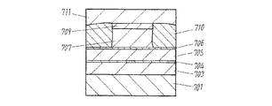
701 n型GaAs基板
703 n型AlGaAsクラッド層
704 量子井戸構造の活性層
705 p型AlGaAsクラッド層
706 p型エッチングストップ層
707 p型AlGaAsクラッド層
709 p型GaAsキャップ層
710 電流ブロック層
711 p型GaAsコンタクト層
713 リッジ型ストライプパターン
901 n側電極
902 n型GaAs基板
903 n型(Al0.7Ga0.3)0.5In0.5Pクラッド層
904 GaInP/AlGaInP多重量子井戸構造活性層
905 n型AlInP電流ブロック層
906 p型GaAsブロック層
907 p型(Al0.7Ga0.3)0.5In0.5Pクラッド層
908 p型GaInPヘテロ緩衝層
909 p型GaAsキャップ層
910 p型GaAsコンタクト層
911 p側電極
913 SiO2ストライプ
Claims (5)
- 基板方位が(001)面から[110]方向に傾斜したオフ角を有する第1導電型半導体基板上に、第1導電型のクラッド層と、活性層と、第2導電型の第1クラッド層と、エッチングストップ層と、第2導電型の第2クラッド層とをこの順に備え、かつ前記第2導電型の第2クラッド層がストライプ状のリッジに形成されている半導体レーザ装置であって、
前記エッチングストップ層は第2導電型の第2クラッド層よりAl含有率が高く、
前記リッジのストライプ方向に垂直な断面形状がほぼ左右対称であり、
前記半導体基板の面方位と前記リッジ型ストライプ側面の面方位とのなす角度が80°以上であり、
前記エッチングストップ層及び前記第2導電型の第2クラッド層がInをさらに含むことを特徴とする半導体レーザ装置。 - 前記リッジの裾にだれが無いことを特徴とする請求項1記載の半導体レーザ装置。
- 前記エッチングストップ層のIn含有率が、前記第2導電型の第2クラッド層のIn含有率よりも高いことを特徴とする請求項1記載の半導体レーザ装置。
- 前記エッチングストップ層はレーザ光を吸収しない程度のバンドギャップを有することを特徴とする請求項1ないし3のいずれかに記載の半導体レーザ装置。
- 前記エッチングストップ層がAlInPまたはAlGaInPを含むことを特徴とする請求項1記載の半導体レーザ装置。
Priority Applications (1)
| Application Number | Priority Date | Filing Date | Title |
|---|---|---|---|
| JP2005102202A JP4331137B2 (ja) | 2005-03-31 | 2005-03-31 | 半導体レーザ |
Applications Claiming Priority (1)
| Application Number | Priority Date | Filing Date | Title |
|---|---|---|---|
| JP2005102202A JP4331137B2 (ja) | 2005-03-31 | 2005-03-31 | 半導体レーザ |
Publications (2)
| Publication Number | Publication Date |
|---|---|
| JP2006286761A JP2006286761A (ja) | 2006-10-19 |
| JP4331137B2 true JP4331137B2 (ja) | 2009-09-16 |
Family
ID=37408364
Family Applications (1)
| Application Number | Title | Priority Date | Filing Date |
|---|---|---|---|
| JP2005102202A Expired - Fee Related JP4331137B2 (ja) | 2005-03-31 | 2005-03-31 | 半導体レーザ |
Country Status (1)
| Country | Link |
|---|---|
| JP (1) | JP4331137B2 (ja) |
-
2005
- 2005-03-31 JP JP2005102202A patent/JP4331137B2/ja not_active Expired - Fee Related
Also Published As
| Publication number | Publication date |
|---|---|
| JP2006286761A (ja) | 2006-10-19 |
Similar Documents
| Publication | Publication Date | Title |
|---|---|---|
| JP3862894B2 (ja) | 半導体レーザ装置 | |
| JP5247444B2 (ja) | 半導体レーザ装置 | |
| US7301979B2 (en) | Semiconductor laser | |
| CN101741016A (zh) | 半导体激光器及其制造方法 | |
| US7221692B2 (en) | Semiconductor laser device and its manufacturing method | |
| US6888870B2 (en) | Semiconductor laser and method for manufacturing the same | |
| US7418019B2 (en) | Multi-wavelength semiconductor laser | |
| US6333946B1 (en) | Semiconductor laser device and process for manufacturing the same | |
| JPWO2006077766A1 (ja) | 半導体レーザ装置及びその製造方法 | |
| JP4751024B2 (ja) | 半導体レーザおよびその製造方法 | |
| JP2007095758A (ja) | 半導体レーザ | |
| JP2004186259A (ja) | 半導体レーザ素子、その製造方法、および多波長集積化半導体レーザ装置 | |
| JP2012222205A (ja) | 半導体レーザ素子及びその製造方法 | |
| JP4331137B2 (ja) | 半導体レーザ | |
| JP2009088441A (ja) | 半導体レーザ装置および半導体レーザ装置の製造方法 | |
| JP2005317572A (ja) | 半導体装置およびその製造方法 | |
| JP2001257431A (ja) | 半導体レーザ | |
| JP4700154B2 (ja) | 半導体レーザ | |
| JP2012238660A (ja) | 窒化物半導体レーザ素子の製造方法 | |
| JP2002151790A (ja) | 半導体レーザおよびその製造方法 | |
| KR20060055696A (ko) | 반도체 레이저 제조방법 | |
| JP2000294877A (ja) | 高出力半導体レーザ及びその製造方法 | |
| JP2014220440A (ja) | 半導体レーザ素子及びその製造方法 | |
| JP2005064262A (ja) | 半導体レーザ素子及びその製造方法 | |
| JP3820826B2 (ja) | 半導体発光装置および半導体装置の製造方法 |
Legal Events
| Date | Code | Title | Description |
|---|---|---|---|
| A977 | Report on retrieval |
Free format text: JAPANESE INTERMEDIATE CODE: A971007 Effective date: 20080904 |
|
| A131 | Notification of reasons for refusal |
Free format text: JAPANESE INTERMEDIATE CODE: A131 Effective date: 20081118 |
|
| RD02 | Notification of acceptance of power of attorney |
Free format text: JAPANESE INTERMEDIATE CODE: A7422 Effective date: 20081217 |
|
| A521 | Written amendment |
Free format text: JAPANESE INTERMEDIATE CODE: A523 Effective date: 20090113 |
|
| RD04 | Notification of resignation of power of attorney |
Free format text: JAPANESE INTERMEDIATE CODE: A7424 Effective date: 20090115 |
|
| TRDD | Decision of grant or rejection written | ||
| A01 | Written decision to grant a patent or to grant a registration (utility model) |
Free format text: JAPANESE INTERMEDIATE CODE: A01 Effective date: 20090519 |
|
| A01 | Written decision to grant a patent or to grant a registration (utility model) |
Free format text: JAPANESE INTERMEDIATE CODE: A01 |
|
| A61 | First payment of annual fees (during grant procedure) |
Free format text: JAPANESE INTERMEDIATE CODE: A61 Effective date: 20090617 |
|
| R150 | Certificate of patent or registration of utility model |
Free format text: JAPANESE INTERMEDIATE CODE: R150 |
|
| FPAY | Renewal fee payment (event date is renewal date of database) |
Free format text: PAYMENT UNTIL: 20120626 Year of fee payment: 3 |
|
| LAPS | Cancellation because of no payment of annual fees |