JP4849821B2 - 表示装置、電子機器 - Google Patents
表示装置、電子機器 Download PDFInfo
- Publication number
- JP4849821B2 JP4849821B2 JP2005128989A JP2005128989A JP4849821B2 JP 4849821 B2 JP4849821 B2 JP 4849821B2 JP 2005128989 A JP2005128989 A JP 2005128989A JP 2005128989 A JP2005128989 A JP 2005128989A JP 4849821 B2 JP4849821 B2 JP 4849821B2
- Authority
- JP
- Japan
- Prior art keywords
- insulating film
- film
- source
- light
- transistor
- Prior art date
- Legal status (The legal status is an assumption and is not a legal conclusion. Google has not performed a legal analysis and makes no representation as to the accuracy of the status listed.)
- Expired - Fee Related
Links
Images


Landscapes
- Electroluminescent Light Sources (AREA)
- Devices For Indicating Variable Information By Combining Individual Elements (AREA)
Description
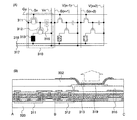
(実施の形態1)
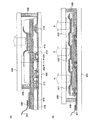
11 トランジスタ
12 第1の絶縁膜
13 第2の絶縁膜
14 第3の絶縁膜
15〜18 ソースドレイン領域
19、21 導電膜
20 電界発光層
22 発光素子
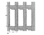
23 絶縁膜
23 隔壁層
26 活性層
27、28 ソースドレイン配線
29、31導電膜
30 電界発光層
32 発光素子
41 第1の絶縁膜
42 第2の絶縁膜
47、48 ソースドレイン配線
49、51 導電膜
50 電界発光層
52 発光素子
53 第3の絶縁膜
61 第1の絶縁膜
62 第2の絶縁膜
63 第3の絶縁膜
64 接続配線
67、68 ソースドレイン配線
69、71 導電膜
70 電界発光層
72 発光素子
73 第4の絶縁膜
81、83 第1の絶縁膜
82、84 第2の絶縁膜、85、86 ソースドレイン配線
Claims (6)
- 基板上に設けられたトランジスタと、
前記トランジスタ上に設けられた、無機材料からなる第1の絶縁膜と、
前記第1の絶縁膜上に設けられた、有機材料からなり、かつ遮光性を有する第2の絶縁膜と、
前記第2の絶縁膜上に設けられた、有機材料からなる第3の絶縁膜と、
前記第1の絶縁膜、前記第2の絶縁膜、及び前記第3の絶縁膜に設けられた開口部を介して、前記トランジスタのソース領域又はドレイン領域に接続されたソースドレイン配線と、
前記ソースドレイン配線上に設けられた、有機材料からなり、かつ遮光性を有する第4の絶縁膜と、
前記第4の絶縁膜に設けられた開口部を介して、前記ソースドレイン配線に接続された接続配線と、
前記接続配線に接する第1の導電膜と、
前記第1の導電膜に接する電界発光層と、
前記電界発光層に接する第2の導電膜と、を有し、
前記ソースドレイン配線と前記接続配線の一方又は両方は、アルミニウムを主成分とし、ニッケルを含む合金材料からなることを特徴とする表示装置。 - 請求項1において、
前記第1の導電膜の端部を囲む隔壁層を有し、
前記隔壁層は第5の絶縁膜と第6の絶縁膜の積層膜からなり、
前記第5の絶縁膜と前記第6の絶縁膜の一方又は両方は、遮光性を有することを特徴とする表示装置。 - 請求項1において、
前記第1の導電膜の端部を囲む隔壁層を有し、
前記隔壁層は第5の絶縁膜と第6の絶縁膜の積層膜からなり、
前記第5の絶縁膜と前記第6の絶縁膜の一方又は両方は、遮光性を有し、
前記第5の絶縁膜と前記第6の絶縁膜は有機材料からなり、前記第5の絶縁膜と前記第6の絶縁膜の一方又は両方は炭素を含むことを特徴とする表示装置。 - 請求項1乃至3のいずれか一項において、
前記合金材料は、炭素と珪素の一方又は両方を含むことを特徴とする表示装置。 - 請求項1乃至4のいずれか一項において、
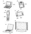
前記第1の導電膜、前記電界発光層及び前記第2の導電膜を含む発光素子は、前記基板と反対の方向に光を発することを特徴とする表示装置。 - 請求項1乃至5のいずれか一項に記載の表示装置を有することを特徴とする電子機器。
Priority Applications (1)
| Application Number | Priority Date | Filing Date | Title |
|---|---|---|---|
| JP2005128989A JP4849821B2 (ja) | 2004-04-28 | 2005-04-27 | 表示装置、電子機器 |
Applications Claiming Priority (3)
| Application Number | Priority Date | Filing Date | Title |
|---|---|---|---|
| JP2004134905 | 2004-04-28 | ||
| JP2004134905 | 2004-04-28 | ||
| JP2005128989A JP4849821B2 (ja) | 2004-04-28 | 2005-04-27 | 表示装置、電子機器 |
Publications (3)
| Publication Number | Publication Date |
|---|---|
| JP2005338812A JP2005338812A (ja) | 2005-12-08 |
| JP2005338812A5 JP2005338812A5 (ja) | 2008-03-21 |
| JP4849821B2 true JP4849821B2 (ja) | 2012-01-11 |
Family
ID=35492404
Family Applications (1)
| Application Number | Title | Priority Date | Filing Date |
|---|---|---|---|
| JP2005128989A Expired - Fee Related JP4849821B2 (ja) | 2004-04-28 | 2005-04-27 | 表示装置、電子機器 |
Country Status (1)
| Country | Link |
|---|---|
| JP (1) | JP4849821B2 (ja) |
Cited By (1)
| Publication number | Priority date | Publication date | Assignee | Title |
|---|---|---|---|---|
| US9985083B2 (en) | 2016-07-01 | 2018-05-29 | Samsung Display Co., Ltd. | Organic light emitting display device and method for manufacturing the same |
Families Citing this family (9)
| Publication number | Priority date | Publication date | Assignee | Title |
|---|---|---|---|---|
| US8148895B2 (en) | 2004-10-01 | 2012-04-03 | Semiconductor Energy Laboratory Co., Ltd. | Display device and manufacturing method of the same |
| JP2007165214A (ja) * | 2005-12-16 | 2007-06-28 | Seiko Epson Corp | エレクトロルミネッセンス装置及び電子機器 |
| US7977862B2 (en) * | 2005-12-21 | 2011-07-12 | Lg Display Co., Ltd. | Organic light emitting devices |
| KR100688792B1 (ko) | 2006-01-27 | 2007-03-02 | 삼성에스디아이 주식회사 | 평판 표시장치 및 그의 제조방법 |
| KR100759666B1 (ko) | 2006-01-27 | 2007-09-17 | 삼성에스디아이 주식회사 | 평판 표시장치 및 그의 제조방법 |
| JP2009076536A (ja) | 2007-09-19 | 2009-04-09 | Mitsubishi Electric Corp | Al合金膜、電子デバイス及び電気光学表示装置用アクティブマトリックス基板 |
| US7977678B2 (en) * | 2007-12-21 | 2011-07-12 | Semiconductor Energy Laboratory Co., Ltd. | Semiconductor display device |
| JP2010135300A (ja) * | 2008-11-10 | 2010-06-17 | Kobe Steel Ltd | 有機elディスプレイ用の反射アノード電極およびその製造方法 |
| JP5141912B2 (ja) * | 2009-02-10 | 2013-02-13 | 三菱マテリアル株式会社 | 上部発光型有機EL素子および前記上部発光型有機EL素子の陽極層を構成する反射膜の形成に用いられるAl合金スパッタリングターゲット |
Family Cites Families (8)
| Publication number | Priority date | Publication date | Assignee | Title |
|---|---|---|---|---|
| JPS62240738A (ja) * | 1986-04-11 | 1987-10-21 | Nippon Mining Co Ltd | 半導体配線材料用n、c含有アルミニウム合金 |
| USRE41975E1 (en) * | 1995-10-12 | 2010-11-30 | Kabushiki Kaisha Toshiba | Interconnector line of thin film, sputter target for forming the wiring film and electronic component using the same |
| JP2000172198A (ja) * | 1998-12-01 | 2000-06-23 | Sanyo Electric Co Ltd | エレクトロルミネッセンス表示装置 |
| JP2002164181A (ja) * | 2000-09-18 | 2002-06-07 | Semiconductor Energy Lab Co Ltd | 表示装置及びその作製方法 |
| JP4090746B2 (ja) * | 2001-01-29 | 2008-05-28 | 株式会社半導体エネルギー研究所 | 発光装置および電子機器 |
| JP2003089864A (ja) * | 2001-09-18 | 2003-03-28 | Mitsui Mining & Smelting Co Ltd | アルミニウム合金薄膜及びその薄膜を有する配線回路並びにその薄膜を形成するターゲット材 |
| JP3904997B2 (ja) * | 2001-09-28 | 2007-04-11 | 株式会社半導体エネルギー研究所 | 発光装置及び電子機器 |
| JP2004071432A (ja) * | 2002-08-08 | 2004-03-04 | Dainippon Printing Co Ltd | パターン形成体およびその製造方法 |
-
2005
- 2005-04-27 JP JP2005128989A patent/JP4849821B2/ja not_active Expired - Fee Related
Cited By (1)
| Publication number | Priority date | Publication date | Assignee | Title |
|---|---|---|---|---|
| US9985083B2 (en) | 2016-07-01 | 2018-05-29 | Samsung Display Co., Ltd. | Organic light emitting display device and method for manufacturing the same |
Also Published As
| Publication number | Publication date |
|---|---|
| JP2005338812A (ja) | 2005-12-08 |
Similar Documents
| Publication | Publication Date | Title |
|---|---|---|
| JP5946878B2 (ja) | 表示装置 | |
| JP5222455B2 (ja) | 表示装置 | |
| JP6517272B2 (ja) | 発光装置 | |
| CN113130587B (zh) | 有机发光二极管显示装置及其制造方法 | |
| US8669925B2 (en) | Light-emitting device and electric appliance | |
| JP4736757B2 (ja) | 発光装置および電子機器 | |
| US8749464B2 (en) | Display device, and method of operation thereof | |
| JP5364227B2 (ja) | 読み取り機能付き表示装置及びそれを用いた電子機器 | |
| CN100414589C (zh) | 电光学装置的制造方法 | |
| CN107978690B (zh) | 显示装置 | |
| KR20210010696A (ko) | 표시 장치 | |
| JP4849821B2 (ja) | 表示装置、電子機器 | |
| US20200144356A1 (en) | Organic light emitting diode display device | |
| KR20200068952A (ko) | 디스플레이 장치 | |
| JP4823651B2 (ja) | 発光装置及びその作製方法 | |
| EP4557912A1 (en) | Display device | |
| CN116386539B (zh) | 显示装置 | |
| US20250204207A1 (en) | Transparent display device | |
| US20250280675A1 (en) | Light Emitting Display Apparatus | |
| US20250266404A1 (en) | Display device | |
| EP4521904A1 (en) | Display device and method of fabricating the same | |
| US20250143098A1 (en) | Display device and method of fabricating the same | |
| US20230209874A1 (en) | Top emission type electroluminescence display having micro-cavity structure | |
| US20240389433A1 (en) | Display device | |
| US20250089530A1 (en) | Display device and method of fabricating the same |
Legal Events
| Date | Code | Title | Description |
|---|---|---|---|
| A521 | Request for written amendment filed |
Free format text: JAPANESE INTERMEDIATE CODE: A523 Effective date: 20080130 |
|
| A621 | Written request for application examination |
Free format text: JAPANESE INTERMEDIATE CODE: A621 Effective date: 20080130 |
|
| A977 | Report on retrieval |
Free format text: JAPANESE INTERMEDIATE CODE: A971007 Effective date: 20110208 |
|
| A131 | Notification of reasons for refusal |
Free format text: JAPANESE INTERMEDIATE CODE: A131 Effective date: 20110322 |
|
| A521 | Request for written amendment filed |
Free format text: JAPANESE INTERMEDIATE CODE: A523 Effective date: 20110401 |
|
| TRDD | Decision of grant or rejection written | ||
| A01 | Written decision to grant a patent or to grant a registration (utility model) |
Free format text: JAPANESE INTERMEDIATE CODE: A01 Effective date: 20111011 |
|
| A01 | Written decision to grant a patent or to grant a registration (utility model) |
Free format text: JAPANESE INTERMEDIATE CODE: A01 |
|
| A61 | First payment of annual fees (during grant procedure) |
Free format text: JAPANESE INTERMEDIATE CODE: A61 Effective date: 20111018 |
|
| R150 | Certificate of patent or registration of utility model |
Ref document number: 4849821 Country of ref document: JP Free format text: JAPANESE INTERMEDIATE CODE: R150 Free format text: JAPANESE INTERMEDIATE CODE: R150 |
|
| FPAY | Renewal fee payment (event date is renewal date of database) |
Free format text: PAYMENT UNTIL: 20141028 Year of fee payment: 3 |
|
| FPAY | Renewal fee payment (event date is renewal date of database) |
Free format text: PAYMENT UNTIL: 20141028 Year of fee payment: 3 |
|
| R250 | Receipt of annual fees |
Free format text: JAPANESE INTERMEDIATE CODE: R250 |
|
| R250 | Receipt of annual fees |
Free format text: JAPANESE INTERMEDIATE CODE: R250 |
|
| R250 | Receipt of annual fees |
Free format text: JAPANESE INTERMEDIATE CODE: R250 |
|
| R250 | Receipt of annual fees |
Free format text: JAPANESE INTERMEDIATE CODE: R250 |
|
| R250 | Receipt of annual fees |
Free format text: JAPANESE INTERMEDIATE CODE: R250 |
|
| R250 | Receipt of annual fees |
Free format text: JAPANESE INTERMEDIATE CODE: R250 |
|
| LAPS | Cancellation because of no payment of annual fees |