JP5209196B2 - 半導体装置の製造方法 - Google Patents
半導体装置の製造方法 Download PDFInfo
- Publication number
- JP5209196B2 JP5209196B2 JP2006301719A JP2006301719A JP5209196B2 JP 5209196 B2 JP5209196 B2 JP 5209196B2 JP 2006301719 A JP2006301719 A JP 2006301719A JP 2006301719 A JP2006301719 A JP 2006301719A JP 5209196 B2 JP5209196 B2 JP 5209196B2
- Authority
- JP
- Japan
- Prior art keywords
- insulating film
- interlayer insulating
- film
- semiconductor device
- manufacturing
- Prior art date
- Legal status (The legal status is an assumption and is not a legal conclusion. Google has not performed a legal analysis and makes no representation as to the accuracy of the status listed.)
- Active
Links
Images


Classifications
-
- H—ELECTRICITY
- H10—SEMICONDUCTOR DEVICES; ELECTRIC SOLID-STATE DEVICES NOT OTHERWISE PROVIDED FOR
- H10D—INORGANIC ELECTRIC SEMICONDUCTOR DEVICES
- H10D30/00—Field-effect transistors [FET]
- H10D30/60—Insulated-gate field-effect transistors [IGFET]
- H10D30/791—Arrangements for exerting mechanical stress on the crystal lattice of the channel regions
- H10D30/792—Arrangements for exerting mechanical stress on the crystal lattice of the channel regions comprising applied insulating layers, e.g. stress liners
-
- H—ELECTRICITY
- H10—SEMICONDUCTOR DEVICES; ELECTRIC SOLID-STATE DEVICES NOT OTHERWISE PROVIDED FOR
- H10D—INORGANIC ELECTRIC SEMICONDUCTOR DEVICES
- H10D84/00—Integrated devices formed in or on semiconductor substrates that comprise only semiconducting layers, e.g. on Si wafers or on GaAs-on-Si wafers
- H10D84/01—Manufacture or treatment
- H10D84/0123—Integrating together multiple components covered by H10D12/00 or H10D30/00, e.g. integrating multiple IGBTs
- H10D84/0126—Integrating together multiple components covered by H10D12/00 or H10D30/00, e.g. integrating multiple IGBTs the components including insulated gates, e.g. IGFETs
- H10D84/0165—Integrating together multiple components covered by H10D12/00 or H10D30/00, e.g. integrating multiple IGBTs the components including insulated gates, e.g. IGFETs the components including complementary IGFETs, e.g. CMOS devices
- H10D84/0167—Manufacturing their channels
-
- H—ELECTRICITY
- H10—SEMICONDUCTOR DEVICES; ELECTRIC SOLID-STATE DEVICES NOT OTHERWISE PROVIDED FOR
- H10D—INORGANIC ELECTRIC SEMICONDUCTOR DEVICES
- H10D84/00—Integrated devices formed in or on semiconductor substrates that comprise only semiconducting layers, e.g. on Si wafers or on GaAs-on-Si wafers
- H10D84/01—Manufacture or treatment
- H10D84/0123—Integrating together multiple components covered by H10D12/00 or H10D30/00, e.g. integrating multiple IGBTs
- H10D84/0126—Integrating together multiple components covered by H10D12/00 or H10D30/00, e.g. integrating multiple IGBTs the components including insulated gates, e.g. IGFETs
- H10D84/0165—Integrating together multiple components covered by H10D12/00 or H10D30/00, e.g. integrating multiple IGBTs the components including insulated gates, e.g. IGFETs the components including complementary IGFETs, e.g. CMOS devices
- H10D84/0184—Manufacturing their gate sidewall spacers
-
- H—ELECTRICITY
- H10—SEMICONDUCTOR DEVICES; ELECTRIC SOLID-STATE DEVICES NOT OTHERWISE PROVIDED FOR
- H10D—INORGANIC ELECTRIC SEMICONDUCTOR DEVICES
- H10D84/00—Integrated devices formed in or on semiconductor substrates that comprise only semiconducting layers, e.g. on Si wafers or on GaAs-on-Si wafers
- H10D84/01—Manufacture or treatment
- H10D84/02—Manufacture or treatment characterised by using material-based technologies
- H10D84/03—Manufacture or treatment characterised by using material-based technologies using Group IV technology, e.g. silicon technology or silicon-carbide [SiC] technology
- H10D84/038—Manufacture or treatment characterised by using material-based technologies using Group IV technology, e.g. silicon technology or silicon-carbide [SiC] technology using silicon technology, e.g. SiGe
-
- H—ELECTRICITY
- H10—SEMICONDUCTOR DEVICES; ELECTRIC SOLID-STATE DEVICES NOT OTHERWISE PROVIDED FOR
- H10W—GENERIC PACKAGES, INTERCONNECTIONS, CONNECTORS OR OTHER CONSTRUCTIONAL DETAILS OF DEVICES COVERED BY CLASS H10
- H10W20/00—Interconnections in chips, wafers or substrates
- H10W20/01—Manufacture or treatment
- H10W20/071—Manufacture or treatment of dielectric parts thereof
- H10W20/093—Manufacture or treatment of dielectric parts thereof by modifying materials of the dielectric parts
- H10W20/095—Manufacture or treatment of dielectric parts thereof by modifying materials of the dielectric parts by irradiating with electromagnetic or particle radiation
-
- H—ELECTRICITY
- H10—SEMICONDUCTOR DEVICES; ELECTRIC SOLID-STATE DEVICES NOT OTHERWISE PROVIDED FOR
- H10W—GENERIC PACKAGES, INTERCONNECTIONS, CONNECTORS OR OTHER CONSTRUCTIONAL DETAILS OF DEVICES COVERED BY CLASS H10
- H10W20/00—Interconnections in chips, wafers or substrates
- H10W20/01—Manufacture or treatment
- H10W20/071—Manufacture or treatment of dielectric parts thereof
- H10W20/093—Manufacture or treatment of dielectric parts thereof by modifying materials of the dielectric parts
- H10W20/096—Manufacture or treatment of dielectric parts thereof by modifying materials of the dielectric parts by contacting with gases, liquids or plasmas
-
- H—ELECTRICITY
- H10—SEMICONDUCTOR DEVICES; ELECTRIC SOLID-STATE DEVICES NOT OTHERWISE PROVIDED FOR
- H10W—GENERIC PACKAGES, INTERCONNECTIONS, CONNECTORS OR OTHER CONSTRUCTIONAL DETAILS OF DEVICES COVERED BY CLASS H10
- H10W20/00—Interconnections in chips, wafers or substrates
- H10W20/01—Manufacture or treatment
- H10W20/071—Manufacture or treatment of dielectric parts thereof
- H10W20/093—Manufacture or treatment of dielectric parts thereof by modifying materials of the dielectric parts
- H10W20/097—Manufacture or treatment of dielectric parts thereof by modifying materials of the dielectric parts by thermally treating
Landscapes
- Metal-Oxide And Bipolar Metal-Oxide Semiconductor Integrated Circuits (AREA)
- Insulated Gate Type Field-Effect Transistor (AREA)
- Thin Film Transistor (AREA)
- Internal Circuitry In Semiconductor Integrated Circuit Devices (AREA)
Description
最近、高性能MOSトランジスタを実現するため、チャネル領域にチャネルストレスを提供してキャリアの移動度(mobility)を向上させる方法が研究されている(特許文献1,2、非特許文献1,2)。
NMOSトランジスタ上に所定引張ストレスを有するライナ膜を形成し、ライナ膜上に第1層間絶縁膜としてO3-TEOS膜を形成した後、第1層間絶縁膜をFT-IR(Fourier Transform-Infrared Spectrometers)を用いて成分を分析した。引き続き、NMOSトランジスタ上に形成された第1層間絶縁膜をO3プラズマ処理した後、第1層間絶縁膜のFT-IRを用いて成分を分析した。その結果が図10に図示されている。
第1ないし第4NMOSトランジスタ上に所定引張ストレスを有するライナ膜を形成し、ライナ膜上に第1層間絶縁膜としてO3-TEOS膜を形成した後、第1層間絶縁膜のストレス大きさを各々測定した(As-Depo)。引き続き、第1ないし第4NMOSトランジスタ上に形成された第1層間絶縁膜を各々NH3プラズマ処理、O3プラズマ処理、N2プラズマ処理、O3プラズマ処理後、N2プラズマ処理して、第1層間絶縁膜のストレス大きさを各々測定した(Treatment)。その結果が、図11にともに図示されている。
シミュレーションプログラムにNMOSトランジスタ上に所定の引張ストレスを有するライナ膜を位置し、ライナ膜上に所定の引張ストレスを有した第1層間絶縁膜が位置するように設定した。その後、第1層間絶縁膜の厚さを変更させながら、それによる電子の移動度変化(mobility change)をシミュレーションした。その結果が、図12に図示されている。
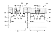
10 半導体基板
20 素子分離領域
30 第1アクチブ領域
32 Pウェル
40 第2アクチブ領域
42 Nウェル
100 NMOSトランジスタ
110 第1ゲート絶縁膜
120 第1ゲート電極
130 スペーサ
146 チャネル領域
160 ソース/ドレイン領域
200 PMOSトランジスタ
210 第2ゲート絶縁膜
220 第2ゲート電極
230 スペーサ
246 チャネル領域
260 ソース/ドレイン領域
310 第1ライナ膜
312 第2ライナ膜
320 第1層間絶縁膜
400 プラズマ処理
Claims (8)
- 基板上にNMOSトランジスタを形成する工程と、
前記NMOSトランジスタ上に引張ストレスを有するライナ膜を形成する工程と、
前記ライナ膜上に第1層間絶縁膜を形成する工程と、
前記第1層間絶縁膜を脱水素化する工程とを含み、
前記NMOSトランジスタは、ゲート絶縁膜及びゲート電極を含み、前記ゲート絶縁膜、前記ゲート電極及び前記ライナ膜の総厚さをt1とし、前記ライナ膜及び前記第1層間絶縁膜の総厚さをt2とする時、t2/t1≧ 1.14であることを特徴とする半導体装置の製造方法。 - 前記第1層間絶縁膜を脱水素化する工程は、前記第1層間絶縁膜のストレスを変化させることを特徴とする請求項1に記載の半導体装置の製造方法。
- 前記第1層間絶縁膜を脱水素化する工程は、前記第1層間絶縁膜を脱水素化ガス雰囲気でプラズマ処理、UV処理及び/または熱処理する工程を含むことを特徴とする請求項1に記載の半導体装置の製造方法。
- 前記脱水素化ガスは、N2、O2、O3、N2O、H2及び/またはD2と、これらの組合わせを含むことを特徴とする請求項3に記載の半導体装置の製造方法。
- 脱水素化の後、前記第1層間絶縁膜は、少なくとも200MPaの引張ストレスを有することを特徴とする請求項1に記載の半導体装置の製造方法。
- 前記第1層間絶縁膜は、O3-TEOS、NSG、PSG、BSG、BPSG、FSG、SOG及び/またはTOSZを含むことを特徴とする請求項1に記載の半導体装置の製造方法。
- 前記第1層間絶縁膜を形成した後、前記第1層間絶縁膜内に前記NMOSトランジスタと接続されるコンタクトを形成する工程をさらに含むことを特徴とする請求項1に記載の半導体装置の製造方法。
- 前記第1層間絶縁膜を脱水素化した後、前記第1層間絶縁膜上に第2層間絶縁膜を形成する工程をさらに含み、前記第2層間絶縁膜は前記第1層間絶縁膜のストレスより小さなストレスを有することを特徴とする請求項1に記載の半導体装置の製造方法。
Applications Claiming Priority (4)
| Application Number | Priority Date | Filing Date | Title |
|---|---|---|---|
| KR1020050106096A KR100678636B1 (ko) | 2005-11-07 | 2005-11-07 | 반도체 집적 회로 장치의 제조 방법 및 그에 의해 제조된반도체 집적 회로 장치 |
| KR10-2005-0106096 | 2005-11-07 | ||
| KR10-2006-0073912 | 2006-08-04 | ||
| KR1020060073912A KR100834737B1 (ko) | 2006-08-04 | 2006-08-04 | 반도체 집적 회로 장치의 제조 방법 및 그에 의해 제조된반도체 집적 회로 장치 |
Publications (3)
| Publication Number | Publication Date |
|---|---|
| JP2007134712A JP2007134712A (ja) | 2007-05-31 |
| JP2007134712A5 JP2007134712A5 (ja) | 2009-12-24 |
| JP5209196B2 true JP5209196B2 (ja) | 2013-06-12 |
Family
ID=38004288
Family Applications (1)
| Application Number | Title | Priority Date | Filing Date |
|---|---|---|---|
| JP2006301719A Active JP5209196B2 (ja) | 2005-11-07 | 2006-11-07 | 半導体装置の製造方法 |
Country Status (3)
| Country | Link |
|---|---|
| US (2) | US7867867B2 (ja) |
| JP (1) | JP5209196B2 (ja) |
| TW (1) | TWI338335B (ja) |
Families Citing this family (24)
| Publication number | Priority date | Publication date | Assignee | Title |
|---|---|---|---|---|
| JP2007324391A (ja) * | 2006-06-01 | 2007-12-13 | Matsushita Electric Ind Co Ltd | 半導体装置及びその製造方法 |
| DE102006030264B4 (de) * | 2006-06-30 | 2008-08-28 | Advanced Micro Devices, Inc., Sunnyvale | Verfahren zur Herstellung von Transistoren mit einem Kanal mit biaxialer Verformung, die durch Silizium/Germanium in der Gateelektrode hervorgerufen wird |
| US20080138983A1 (en) * | 2006-12-06 | 2008-06-12 | Taiwan Semiconductor Manufacturing Co., Ltd. | Method of forming tensile stress films for NFET performance enhancement |
| US20080206943A1 (en) * | 2007-02-26 | 2008-08-28 | Jei-Ming Chen | Method of forming strained cmos transistor |
| JP2008235636A (ja) * | 2007-03-22 | 2008-10-02 | Elpida Memory Inc | 半導体装置の製造方法及び半導体装置 |
| US7741171B2 (en) * | 2007-05-15 | 2010-06-22 | Taiwan Semiconductor Manufacturing Company, Ltd. | Oxygen-rich layers underlying BPSG |
| US8072035B2 (en) | 2007-06-11 | 2011-12-06 | Renesas Electronics Corporation | Semiconductor device and method of manufacturing the same |
| JP5280716B2 (ja) * | 2007-06-11 | 2013-09-04 | ルネサスエレクトロニクス株式会社 | 半導体装置およびその製造方法 |
| US7911001B2 (en) | 2007-07-15 | 2011-03-22 | Samsung Electronics Co., Ltd. | Methods for forming self-aligned dual stress liners for CMOS semiconductor devices |
| US7858532B2 (en) | 2007-08-06 | 2010-12-28 | United Microelectronics Corp. | Dielectric layer structure and manufacturing method thereof |
| US8466508B2 (en) * | 2007-10-03 | 2013-06-18 | Macronix International Co., Ltd. | Non-volatile memory structure including stress material between stacked patterns |
| DE102007057686B4 (de) * | 2007-11-30 | 2011-07-28 | GLOBALFOUNDRIES Dresden Module One Ltd. Liability Company & Co. KG, 01109 | Verfahren und Halbleiterbauelement mit einer Schutzschicht zum Reduzieren der Verspannungsrelaxation in einer Doppelverspannungsbeschichtungstechnik |
| US8211784B2 (en) * | 2009-10-26 | 2012-07-03 | Advanced Ion Beam Technology, Inc. | Method for manufacturing a semiconductor device with less leakage current induced by carbon implant |
| JP5652939B2 (ja) * | 2010-07-07 | 2015-01-14 | ルネサスエレクトロニクス株式会社 | 半導体装置及び半導体装置の製造方法 |
| CN102569083B (zh) * | 2010-12-23 | 2014-12-24 | 中芯国际集成电路制造(上海)有限公司 | 具有高k金属栅极的金属氧化物半导体的形成方法 |
| US8853862B2 (en) * | 2011-12-20 | 2014-10-07 | International Business Machines Corporation | Contact structures for semiconductor transistors |
| US9177803B2 (en) * | 2013-03-14 | 2015-11-03 | Globalfoundries Inc. | HK/MG process flows for P-type semiconductor devices |
| US9252271B2 (en) * | 2013-11-27 | 2016-02-02 | Taiwan Semiconductor Manufacturing Company Limited | Semiconductor device and method of making |
| KR102292813B1 (ko) * | 2015-10-14 | 2021-08-23 | 삼성전자주식회사 | 반도체 장치 및 이의 제조 방법 |
| US10020401B2 (en) * | 2016-11-29 | 2018-07-10 | Taiwan Semiconductor Manufacturing Company, Ltd. | Methods for straining a transistor gate through interlayer dielectric (ILD) doping schemes |
| FR3076077B1 (fr) * | 2017-12-22 | 2020-02-28 | Commissariat A L'energie Atomique Et Aux Energies Alternatives | Realisation de transistors a canaux contraints |
| JP7355752B2 (ja) * | 2018-10-05 | 2023-10-03 | 株式会社半導体エネルギー研究所 | 半導体装置の作製方法 |
| CN109686663A (zh) * | 2018-12-27 | 2019-04-26 | 上海华力微电子有限公司 | 一种半导体结构及其制造方法 |
| KR102793906B1 (ko) | 2020-06-10 | 2025-04-08 | 삼성전자주식회사 | 집적회로 장치 |
Family Cites Families (20)
| Publication number | Priority date | Publication date | Assignee | Title |
|---|---|---|---|---|
| JPS5730337A (en) * | 1980-07-30 | 1982-02-18 | Nec Corp | Formation of surface protecting film for semiconductor |
| JP2885458B2 (ja) * | 1990-02-27 | 1999-04-26 | 株式会社東芝 | 薄膜トランジスタ |
| JPH04345069A (ja) * | 1991-05-22 | 1992-12-01 | Oki Electric Ind Co Ltd | 半導体装置 |
| JP2758847B2 (ja) * | 1995-02-08 | 1998-05-28 | 日本電気株式会社 | スピンオングラス膜の形成方法 |
| KR100289194B1 (ko) | 1996-06-29 | 2001-05-02 | 이구택 | 고로 슬러지를 전로 스크랩으로 재활용하는 방법 |
| JPH10173075A (ja) | 1996-12-05 | 1998-06-26 | Sanyo Electric Co Ltd | 半導体装置の製造方法及び半導体記憶装置の製造方法 |
| JP3745863B2 (ja) | 1997-02-28 | 2006-02-15 | 芝浦メカトロニクス株式会社 | ウエットエッチング処理方法およびその処理装置 |
| JP2000164716A (ja) * | 1998-11-26 | 2000-06-16 | Seiko Epson Corp | 半導体装置及びその製造方法 |
| JP3562357B2 (ja) * | 1998-12-22 | 2004-09-08 | セイコーエプソン株式会社 | 半導体装置の製造方法 |
| US6821827B2 (en) | 1999-12-28 | 2004-11-23 | Semiconductor Energy Laboratory Co., Ltd. | Method of manufacturing a semiconductor device |
| JP2001250956A (ja) * | 2000-03-08 | 2001-09-14 | Semiconductor Energy Lab Co Ltd | 半導体装置 |
| KR100784603B1 (ko) * | 2000-11-22 | 2007-12-11 | 가부시키가이샤 히타치세이사쿠쇼 | 반도체 장치 및 그 제조 방법 |
| KR100391992B1 (ko) | 2000-12-08 | 2003-07-22 | 삼성전자주식회사 | 저유전율 층간절연막을 가지는 반도체 장치 형성 방법 |
| JP4557508B2 (ja) | 2003-06-16 | 2010-10-06 | パナソニック株式会社 | 半導体装置 |
| TWI235458B (en) | 2003-07-02 | 2005-07-01 | Taiwan Semiconductor Mfg | MOS transistor and fabrication method thereof |
| JP4683833B2 (ja) * | 2003-10-31 | 2011-05-18 | 株式会社半導体エネルギー研究所 | 機能回路及びその設計方法 |
| JP4322687B2 (ja) * | 2004-01-09 | 2009-09-02 | エルピーダメモリ株式会社 | 半導体装置の製造方法 |
| US20050186722A1 (en) * | 2004-02-25 | 2005-08-25 | Kuan-Lun Cheng | Method and structure for CMOS device with stress relaxed by ion implantation of carbon or oxygen containing ions |
| KR101025761B1 (ko) * | 2004-03-30 | 2011-04-04 | 삼성전자주식회사 | 디지탈 회로 및 아날로그 회로를 가지는 반도체 집적회로및 그 제조 방법 |
| DE102004026149B4 (de) * | 2004-05-28 | 2008-06-26 | Advanced Micro Devices, Inc., Sunnyvale | Verfahren zum Erzeugen eines Halbleiterbauelements mit Transistorelementen mit spannungsinduzierenden Ätzstoppschichten |
-
2006
- 2006-11-07 US US11/593,898 patent/US7867867B2/en active Active
- 2006-11-07 JP JP2006301719A patent/JP5209196B2/ja active Active
- 2006-11-07 TW TW095141118A patent/TWI338335B/zh active
-
2011
- 2011-01-10 US US12/987,415 patent/US8237202B2/en active Active
Also Published As
| Publication number | Publication date |
|---|---|
| US20110163386A1 (en) | 2011-07-07 |
| US7867867B2 (en) | 2011-01-11 |
| US20070105297A1 (en) | 2007-05-10 |
| US8237202B2 (en) | 2012-08-07 |
| JP2007134712A (ja) | 2007-05-31 |
| TW200729353A (en) | 2007-08-01 |
| TWI338335B (en) | 2011-03-01 |
Similar Documents
| Publication | Publication Date | Title |
|---|---|---|
| JP5209196B2 (ja) | 半導体装置の製造方法 | |
| US7534678B2 (en) | Methods of forming CMOS integrated circuit devices having stressed NMOS and PMOS channel regions therein and circuits formed thereby | |
| US8384167B2 (en) | Semiconductor device with field effect transistor and manufacturing method thereof | |
| US8084787B2 (en) | PMD liner nitride films and fabrication methods for improved NMOS performance | |
| US20120252198A1 (en) | Method for manufacturing semiconductor structure | |
| US7888214B2 (en) | Selective stress relaxation of contact etch stop layer through layout design | |
| JP2007123518A (ja) | 半導体装置およびその製造方法 | |
| US6184114B1 (en) | MOS transistor formation | |
| US20080206943A1 (en) | Method of forming strained cmos transistor | |
| US20070200185A1 (en) | Semiconductor device and method for fabricating the same | |
| US7172936B2 (en) | Method to selectively strain NMOS devices using a cap poly layer | |
| US20080171413A1 (en) | Method of Reducing Detrimental STI-Induced Stress in MOSFET Channels | |
| KR100678636B1 (ko) | 반도체 집적 회로 장치의 제조 방법 및 그에 의해 제조된반도체 집적 회로 장치 | |
| US7714364B2 (en) | Semiconductor device comprising gate electrode having arsenic and phosphorus | |
| JP2011165973A (ja) | 半導体装置及びその製造方法 | |
| KR100834737B1 (ko) | 반도체 집적 회로 장치의 제조 방법 및 그에 의해 제조된반도체 집적 회로 장치 | |
| US8470656B2 (en) | Semiconductor device and method of manufacturing the same | |
| US7192822B2 (en) | Method of fabricating CMOS type semiconductor device having dual gates | |
| US20050142784A1 (en) | Methods of fabricating semiconductor devices | |
| KR100724574B1 (ko) | 식각저지막을 갖는 반도체 소자 및 그의 제조방법 | |
| KR100744248B1 (ko) | 반도체 소자의 제조 방법 | |
| US20070200151A1 (en) | Semiconductor device and method of fabricating the same | |
| KR20050065229A (ko) | 모스 트랜지스터의 제조 방법 | |
| US20020155674A1 (en) | Method for preventing boron penentration of a MOS transistor | |
| JP2005347631A (ja) | 半導体装置の製造方法及び半導体装置。 |
Legal Events
| Date | Code | Title | Description |
|---|---|---|---|
| A521 | Request for written amendment filed |
Free format text: JAPANESE INTERMEDIATE CODE: A523 Effective date: 20091106 |
|
| A621 | Written request for application examination |
Free format text: JAPANESE INTERMEDIATE CODE: A621 Effective date: 20091106 |
|
| A521 | Request for written amendment filed |
Free format text: JAPANESE INTERMEDIATE CODE: A523 Effective date: 20101026 |
|
| A977 | Report on retrieval |
Free format text: JAPANESE INTERMEDIATE CODE: A971007 Effective date: 20120911 |
|
| A131 | Notification of reasons for refusal |
Free format text: JAPANESE INTERMEDIATE CODE: A131 Effective date: 20120918 |
|
| A521 | Request for written amendment filed |
Free format text: JAPANESE INTERMEDIATE CODE: A523 Effective date: 20121217 |
|
| TRDD | Decision of grant or rejection written | ||
| A01 | Written decision to grant a patent or to grant a registration (utility model) |
Free format text: JAPANESE INTERMEDIATE CODE: A01 Effective date: 20130212 |
|
| A61 | First payment of annual fees (during grant procedure) |
Free format text: JAPANESE INTERMEDIATE CODE: A61 Effective date: 20130221 |
|
| FPAY | Renewal fee payment (event date is renewal date of database) |
Free format text: PAYMENT UNTIL: 20160301 Year of fee payment: 3 |
|
| R150 | Certificate of patent or registration of utility model |
Free format text: JAPANESE INTERMEDIATE CODE: R150 Ref document number: 5209196 Country of ref document: JP Free format text: JAPANESE INTERMEDIATE CODE: R150 |
|
| R250 | Receipt of annual fees |
Free format text: JAPANESE INTERMEDIATE CODE: R250 |
|
| R250 | Receipt of annual fees |
Free format text: JAPANESE INTERMEDIATE CODE: R250 |
|
| R250 | Receipt of annual fees |
Free format text: JAPANESE INTERMEDIATE CODE: R250 |
|
| R250 | Receipt of annual fees |
Free format text: JAPANESE INTERMEDIATE CODE: R250 |
|
| R250 | Receipt of annual fees |
Free format text: JAPANESE INTERMEDIATE CODE: R250 |
|
| R250 | Receipt of annual fees |
Free format text: JAPANESE INTERMEDIATE CODE: R250 |
|
| R250 | Receipt of annual fees |
Free format text: JAPANESE INTERMEDIATE CODE: R250 |
|
| R250 | Receipt of annual fees |
Free format text: JAPANESE INTERMEDIATE CODE: R250 |
|
| R250 | Receipt of annual fees |
Free format text: JAPANESE INTERMEDIATE CODE: R250 |
|
| R250 | Receipt of annual fees |
Free format text: JAPANESE INTERMEDIATE CODE: R250 |