JP5583274B2 - コンピュータ・メモリを管理する方法、対応するコンピュータ・プログラム製品、およびそのためのデータ・ストレージ・デバイス - Google Patents
コンピュータ・メモリを管理する方法、対応するコンピュータ・プログラム製品、およびそのためのデータ・ストレージ・デバイス Download PDFInfo
- Publication number
- JP5583274B2 JP5583274B2 JP2013523548A JP2013523548A JP5583274B2 JP 5583274 B2 JP5583274 B2 JP 5583274B2 JP 2013523548 A JP2013523548 A JP 2013523548A JP 2013523548 A JP2013523548 A JP 2013523548A JP 5583274 B2 JP5583274 B2 JP 5583274B2
- Authority
- JP
- Japan
- Prior art keywords
- data
- cache
- memory
- data block
- page table
- Prior art date
- Legal status (The legal status is an assumption and is not a legal conclusion. Google has not performed a legal analysis and makes no representation as to the accuracy of the status listed.)
- Expired - Fee Related
Links
Images
Classifications
-
- G—PHYSICS
- G06—COMPUTING OR CALCULATING; COUNTING
- G06F—ELECTRIC DIGITAL DATA PROCESSING
- G06F12/00—Accessing, addressing or allocating within memory systems or architectures
- G06F12/02—Addressing or allocation; Relocation
- G06F12/08—Addressing or allocation; Relocation in hierarchically structured memory systems, e.g. virtual memory systems
- G06F12/10—Address translation
- G06F12/1009—Address translation using page tables, e.g. page table structures
-
- G—PHYSICS
- G06—COMPUTING OR CALCULATING; COUNTING
- G06F—ELECTRIC DIGITAL DATA PROCESSING
- G06F12/00—Accessing, addressing or allocating within memory systems or architectures
- G06F12/02—Addressing or allocation; Relocation
- G06F12/08—Addressing or allocation; Relocation in hierarchically structured memory systems, e.g. virtual memory systems
-
- G—PHYSICS
- G06—COMPUTING OR CALCULATING; COUNTING
- G06F—ELECTRIC DIGITAL DATA PROCESSING
- G06F12/00—Accessing, addressing or allocating within memory systems or architectures
- G06F12/14—Protection against unauthorised use of memory or access to memory
-
- G—PHYSICS
- G06—COMPUTING OR CALCULATING; COUNTING
- G06F—ELECTRIC DIGITAL DATA PROCESSING
- G06F9/00—Arrangements for program control, e.g. control units
- G06F9/06—Arrangements for program control, e.g. control units using stored programs, i.e. using an internal store of processing equipment to receive or retain programs
- G06F9/46—Multiprogramming arrangements
-
- G—PHYSICS
- G06—COMPUTING OR CALCULATING; COUNTING
- G06F—ELECTRIC DIGITAL DATA PROCESSING
- G06F12/00—Accessing, addressing or allocating within memory systems or architectures
- G06F12/14—Protection against unauthorised use of memory or access to memory
- G06F12/1416—Protection against unauthorised use of memory or access to memory by checking the object accessibility, e.g. type of access defined by the memory independently of subject rights
- G06F12/145—Protection against unauthorised use of memory or access to memory by checking the object accessibility, e.g. type of access defined by the memory independently of subject rights the protection being virtual, e.g. for virtual blocks or segments before a translation mechanism
-
- G—PHYSICS
- G06—COMPUTING OR CALCULATING; COUNTING
- G06F—ELECTRIC DIGITAL DATA PROCESSING
- G06F2212/00—Indexing scheme relating to accessing, addressing or allocation within memory systems or architectures
- G06F2212/10—Providing a specific technical effect
- G06F2212/1016—Performance improvement
-
- G—PHYSICS
- G06—COMPUTING OR CALCULATING; COUNTING
- G06F—ELECTRIC DIGITAL DATA PROCESSING
- G06F2212/00—Indexing scheme relating to accessing, addressing or allocation within memory systems or architectures
- G06F2212/10—Providing a specific technical effect
- G06F2212/1052—Security improvement
Landscapes
- Engineering & Computer Science (AREA)
- Theoretical Computer Science (AREA)
- Physics & Mathematics (AREA)
- General Engineering & Computer Science (AREA)
- General Physics & Mathematics (AREA)
- Software Systems (AREA)
- Computer Security & Cryptography (AREA)
- Memory System Of A Hierarchy Structure (AREA)
Description
Claims (10)
- コンピュータ・メモリを管理する方法であって、
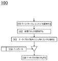
仮想アドレスを物理アドレスにマップするためのページ・テーブル・エントリー、および複数のデータ・ブロックを含むキャッシュを保持するステップ(101)と、
前記仮想アドレスへの参照に応答して、前記ページ・テーブル・エントリーを用いて前記仮想アドレスを前記物理アドレスへと変換するステップ(102)と、データを前記物理アドレスから前記キャッシュ内へフェッチするステップ(103)と
を含む方法において、前記ページ・テーブル・エントリーが、複数のインジケータを含み、それぞれのデータ・ブロックが、前記複数のインジケータのうちの1つに対応し、前記データを前記キャッシュ内へフェッチするステップ(103)が開始すると、当該方法が、
前記複数のインジケータから選択された1つのインジケータ(110)がセットされていることに応答して、前記対応するデータ・ブロックをゼロ化するさらなるステップ(104)を含むことを特徴とする方法。
- 前記ページ・テーブル・エントリーがビットマスクを含み、前記インジケータが、前記ビットマスク内に含まれているビットであることを特徴とする、請求項1に記載の方法。
- 前記ページ・テーブル・エントリーが、前記複数のデータ・ブロックを含むメモリ・ページに関連付けられ、前記方法が、
データ・ブロックを受け取る中間ステップと、
前記データ・ブロックを前記メモリ・ページ内に格納する中間ステップと、
前記データ・ブロックが対応する前記インジケータをクリアする中間ステップとを含むことを特徴とする、請求項1に記載の方法。
- 前記データ・ブロックが対応していない、前記複数のインジケータのうちの残りのインジケータをセットするさらなるステップ
を含むことを特徴とする、請求項1に記載の方法。
- さらなるデータ・ブロックを上書きする後続ステップと、
前記さらなるデータ・ブロックが対応する前記インジケータをクリアする後続ステップと
を含むことを特徴とする、請求項3または4に記載の方法。
- コンピュータ・プログラムであって、プログラムがコンピュータ上で実行されたときに請求項1に記載の方法を実行するためのコンピュータ実行可能命令を含む、コンピュータ・プログラム。
- オペレーティング・システムを含むことを特徴とする、請求項6に記載のコンピュータ・プログラム。
- 仮想アドレスを物理アドレスにマップするためのページ・テーブル・エントリー、および複数のデータ・ブロックを含むキャッシュを保持するステップ(101)を行うための手段と、
前記仮想アドレスへの参照に応答して、前記ページ・テーブル・エントリーを用いて前記仮想アドレスを前記物理アドレスへと変換するステップ(102)、およびデータを前記物理アドレスから前記キャッシュ内へフェッチするステップ(103)を行うための手段と
を含むデバイスにおいて、前記ページ・テーブル・エントリーが、複数のインジケータを含み、それぞれのデータ・ブロックが、前記複数のインジケータのうちの1つに対応し、当該デバイスが、前記データを前記キャッシュ内へフェッチするステップ(103)が開始されると、
前記複数のインジケータから選択された1つのインジケータ(110)がセットされていることに応答して、前記対応するデータ・ブロックをゼロ化するステップ(104)を行うためのさらなる手段を含むことを特徴とするデバイス。
- 中央処理装置、
メモリ・マネージメント・ユニット、および
データ・キャッシュ
のうちの少なくとも1つを含むことを特徴とする、請求項8に記載のデバイス。
- 前記ページ・テーブル・エントリーを格納するように構成されている変換ルックアサイド・バッファをさらに含み、前記仮想アドレスが、前記変換ルックアサイド・バッファを用いて変換される(102)ことを特徴とする、請求項8または9に記載のデバイス。
Applications Claiming Priority (3)
| Application Number | Priority Date | Filing Date | Title |
|---|---|---|---|
| EP10305868.1 | 2010-08-06 | ||
| EP10305868A EP2416251B1 (en) | 2010-08-06 | 2010-08-06 | A method of managing computer memory, corresponding computer program product, and data storage device therefor |
| PCT/EP2011/061513 WO2012016783A1 (en) | 2010-08-06 | 2011-07-07 | A method of managing computer memory, corresponding computer program product; and data storage device therefor |
Publications (2)
| Publication Number | Publication Date |
|---|---|
| JP2013544380A JP2013544380A (ja) | 2013-12-12 |
| JP5583274B2 true JP5583274B2 (ja) | 2014-09-03 |
Family
ID=43569401
Family Applications (1)
| Application Number | Title | Priority Date | Filing Date |
|---|---|---|---|
| JP2013523548A Expired - Fee Related JP5583274B2 (ja) | 2010-08-06 | 2011-07-07 | コンピュータ・メモリを管理する方法、対応するコンピュータ・プログラム製品、およびそのためのデータ・ストレージ・デバイス |
Country Status (6)
| Country | Link |
|---|---|
| US (1) | US20130124821A1 (ja) |
| EP (1) | EP2416251B1 (ja) |
| JP (1) | JP5583274B2 (ja) |
| KR (1) | KR101451045B1 (ja) |
| CN (1) | CN103052945B (ja) |
| WO (1) | WO2012016783A1 (ja) |
Families Citing this family (11)
| Publication number | Priority date | Publication date | Assignee | Title |
|---|---|---|---|---|
| CN105359115A (zh) * | 2013-07-01 | 2016-02-24 | 惠普发展公司,有限责任合伙企业 | 包含虚拟地址空间和物理地址空间之间的映射的数据结构的查找 |
| CN104699633B (zh) * | 2013-12-04 | 2019-04-23 | 瑞昱半导体股份有限公司 | 虚拟物理地址转换系统及其管理方法 |
| WO2016106757A1 (zh) * | 2014-12-31 | 2016-07-07 | 华为技术有限公司 | 一种存储数据的管理方法、存储管理器及存储系统 |
| KR101994952B1 (ko) | 2015-03-27 | 2019-07-01 | 후아웨이 테크놀러지 컴퍼니 리미티드 | 데이터 처리 방법, 메모리 관리 유닛, 및 메모리 제어 장치 |
| WO2016171866A1 (en) * | 2015-04-24 | 2016-10-27 | Optimum Semiconductor Technologies, Inc. | Computer processor with separate registers for addressing memory |
| US10884945B2 (en) * | 2015-06-30 | 2021-01-05 | International Business Machines Corporation | Memory state indicator check operations |
| WO2017058218A1 (en) * | 2015-09-30 | 2017-04-06 | Hewlett Packard Enterprise Development LP. | Using a memory controller to manage access to a memory based on a memory initialization state indicator |
| US10534724B2 (en) * | 2015-12-24 | 2020-01-14 | Intel Corporation | Instructions and logic to suspend/resume migration of enclaves in a secure enclave page cache |
| CN112486403B (zh) * | 2019-09-12 | 2024-12-24 | 伊姆西Ip控股有限责任公司 | 管理存储对象的元数据的方法、装置和计算机程序产品 |
| CN112799977B (zh) * | 2021-02-26 | 2022-07-19 | 中国人民解放军国防科技大学 | 计算机的缓存分区和缓存访问实时性保护方法及装置 |
| CN115712500A (zh) * | 2022-11-10 | 2023-02-24 | 阿里云计算有限公司 | 内存释放、内存恢复方法、装置、计算机设备及存储介质 |
Family Cites Families (8)
| Publication number | Priority date | Publication date | Assignee | Title |
|---|---|---|---|---|
| JPH02176951A (ja) * | 1988-12-28 | 1990-07-10 | Nec Corp | 仮想記憶装置 |
| US5388244A (en) * | 1992-09-17 | 1995-02-07 | International Business Machines Corporation | Controls for initial diversion of page-frame logical content as part of dynamic virtual-to-real translation of a virtual page address |
| US5920895A (en) * | 1995-04-24 | 1999-07-06 | Microsoft Corporation | Mapped file input/output with delayed zeroing |
| US7073042B2 (en) * | 2002-12-12 | 2006-07-04 | Intel Corporation | Reclaiming existing fields in address translation data structures to extend control over memory accesses |
| US8214622B2 (en) * | 2004-05-27 | 2012-07-03 | International Business Machines Corporation | Facilitating management of storage of a pageable mode virtual environment absent intervention of a host of the environment |
| US20080229117A1 (en) * | 2007-03-07 | 2008-09-18 | Shin Kang G | Apparatus for preventing digital piracy |
| GB2448907B (en) * | 2007-05-02 | 2011-07-27 | Advanced Risc Mach Ltd | Reducng information leakage between processes sharing a cache |
| US7757035B2 (en) * | 2007-06-26 | 2010-07-13 | Intel Corporation | Method for optimizing virtualization technology and memory protections using processor-extensions for page table and page directory striping |
-
2010
- 2010-08-06 EP EP10305868A patent/EP2416251B1/en not_active Not-in-force
-
2011
- 2011-07-07 CN CN201180036120.1A patent/CN103052945B/zh not_active Expired - Fee Related
- 2011-07-07 JP JP2013523548A patent/JP5583274B2/ja not_active Expired - Fee Related
- 2011-07-07 US US13/810,282 patent/US20130124821A1/en not_active Abandoned
- 2011-07-07 WO PCT/EP2011/061513 patent/WO2012016783A1/en not_active Ceased
- 2011-07-07 KR KR1020137005686A patent/KR101451045B1/ko not_active Expired - Fee Related
Also Published As
| Publication number | Publication date |
|---|---|
| JP2013544380A (ja) | 2013-12-12 |
| CN103052945B (zh) | 2015-09-16 |
| CN103052945A (zh) | 2013-04-17 |
| EP2416251B1 (en) | 2013-01-02 |
| WO2012016783A1 (en) | 2012-02-09 |
| US20130124821A1 (en) | 2013-05-16 |
| EP2416251A1 (en) | 2012-02-08 |
| KR20130041303A (ko) | 2013-04-24 |
| KR101451045B1 (ko) | 2014-10-15 |
Similar Documents
| Publication | Publication Date | Title |
|---|---|---|
| JP5583274B2 (ja) | コンピュータ・メモリを管理する方法、対応するコンピュータ・プログラム製品、およびそのためのデータ・ストレージ・デバイス | |
| RU2427892C2 (ru) | Способ и устройство для установки политики кэширования в процессоре | |
| US10802987B2 (en) | Computer processor employing cache memory storing backless cache lines | |
| US9430402B2 (en) | System and method for providing stealth memory | |
| US20190243776A1 (en) | 32-bit address space containment to secure processes from speculative rogue cache loads | |
| US7793070B2 (en) | Processing system implementing multiple page size memory organization with multiple translation lookaside buffers having differing characteristics | |
| EP2017739A1 (en) | Processing system implementing variable page size memory organization | |
| TWI641947B (zh) | 用於管理位址轉換和快取記憶體儲存的方法及裝置 | |
| US9229862B2 (en) | Cache management based on physical memory device characteristics | |
| TWI648625B (zh) | 管理位址獨立的頁面屬性 | |
| US20160259732A1 (en) | Managing reuse information for memory pages | |
| US20170220482A1 (en) | Manipulation of virtual memory page table entries to form virtually-contiguous memory corresponding to non-contiguous real memory allocations | |
| JP2024527054A (ja) | 動的割当可能な物理的にアドレス指定されるメタデータストレージ | |
| US10372622B2 (en) | Software controlled cache line replacement within a data property dependent cache segment of a cache using a cache segmentation enablement bit and cache segment selection bits | |
| CN115618336A (zh) | 缓存及其操作方法、计算机装置 |
Legal Events
| Date | Code | Title | Description |
|---|---|---|---|
| A131 | Notification of reasons for refusal |
Free format text: JAPANESE INTERMEDIATE CODE: A131 Effective date: 20140218 |
|
| A521 | Request for written amendment filed |
Free format text: JAPANESE INTERMEDIATE CODE: A523 Effective date: 20140516 |
|
| TRDD | Decision of grant or rejection written | ||
| A01 | Written decision to grant a patent or to grant a registration (utility model) |
Free format text: JAPANESE INTERMEDIATE CODE: A01 Effective date: 20140617 |
|
| A61 | First payment of annual fees (during grant procedure) |
Free format text: JAPANESE INTERMEDIATE CODE: A61 Effective date: 20140715 |
|
| R150 | Certificate of patent or registration of utility model |
Ref document number: 5583274 Country of ref document: JP Free format text: JAPANESE INTERMEDIATE CODE: R150 |
|
| LAPS | Cancellation because of no payment of annual fees |